

Page 1
DATA SH EET
INTEGRATED CIRCUITS
TDA7056AT
3 W mono BTL audio amplifier with
DC volume control
Product specification 1998 Feb 23
Page 2
NXP Semiconductors Product specification
3 W mono BTL audio amplifier with DC
TDA7056AT
volume control
FEATURES
• DC volume control
• Few external components
• Mute mode
• Thermal protection
• Short-circuit proof
• No switch-on or switch-off clicks
• Good overall stability
• Low power consumption
• Low HF radiation
• ESD protected on all pins.
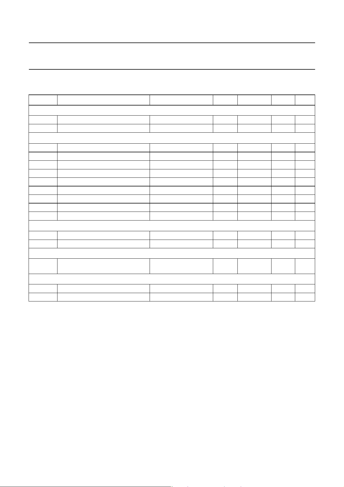
QUICK REFERENCE DATA
SYMBOL PARAMETER CONDITIONS MIN. TYP. MAX. UNIT
V
P
P
o
G
v(max)
ΔG
v
I
q(tot)
THD total harmonic distortion P
supply voltage 4.5 − 18 V
output power VP=12V; RL=16Ω 33.5− W
maximum total voltage gain VP=12V; RL=16Ω 34.5 35.5 36.5 dB
voltage gain control range 75 80 − dB
total quiescent current VP=12V; RL= ∞− 816mA
GENERAL DESCRIPTION
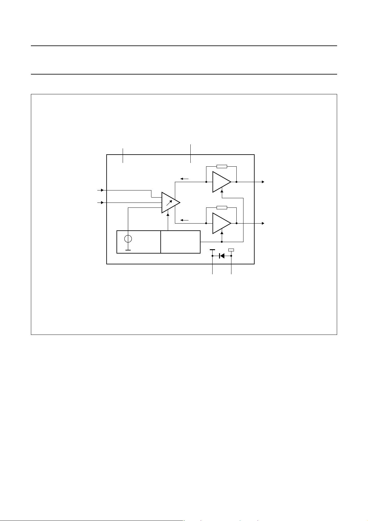
The TDA7056AT is a mono Bridge-Tied Load (BTL) output
amplifier with DC volume control. It is designed for use in
TVs and monitors, but is also suitable for battery-fed
portable recorders and radios. The device is contained in
a 20-lead small outline package.
A Missing Current Limiter (MCL) is built in. The MCL circuit
is activated when the difference in current between the
output terminal of each amplifier exceeds 100 mA
(300 mA typ.). This level of 100 mA allows for
Single-Ended (SE) headphone applications.
=0.5W − 0.3 1 %
o
ORDERING INFORMATION
TYPE
NUMBER
TDA7056AT SO2 0 plastic small outline package with 20 leads; body width 7.5 mm SOT163-1
NAME DESCRIPTION VERSION
PACKAGE
1998 Feb 23 2
Page 3
NXP Semiconductors Product specification
3 W mono BTL audio amplifier with DC
volume control
BLOCK DIAGRAM
handbook, full pagewidth
positive input
DC volume control
5
7
n.c.
1 to 3, 8 to 13,
16, 18 to 20
TDA7056AT
+
V
STABILIZER
ref
+
−
TEMPERATURE
PROTECTION
V
P
4
I + i
TDA7056AT
+
14
17I − i
positive output
−
negative output
ground
Fig.1 Block diagram.
signal
power
ground
15
MGM576
6
1998 Feb 23 3
Page 4

NXP Semiconductors Product specification
3 W mono BTL audio amplifier with DC
volume control
PINNING
SYMBOL PIN DESCRIPTION
n.c. 1 not connected
n.c. 2 not connected
n.c. 3 not connected
V
P
V
I
GND1 6 signal ground
VC 7 DC volume control
n.c. 8 not connected
n.c. 9 not connected
n.c. 10 not connected
n.c. 11 not connected
n.c. 12 not connected
n.c. 13 not connected
OUT+ 14 positive output
GND2 15 power ground
n.c. 16 not connected
OUT− 17 negative output
n.c. 18 not connected
n.c. 19 not connected
n.c. 20 not connected
4 positive supply voltage
5 positive input
handbook, halfpage
n.c.
1
n.c.
2
n.c.
3
V
4
P
V
5
I
VC
n.c.
n.c.
n.c.
TDA7056AT
6
7
8
9
10
MGM577
GND1
Fig.2 Pin configuration.
TDA7056AT
n.c.
20
19
n.c.
18
n.c.
17
OUT−
16
n.c.
GND2
15
OUT+
14
n.c.
13
n.c.
12
n.c.
11
1998 Feb 23 4
Page 5
NXP Semiconductors Product specification
3 W mono BTL audio amplifier with DC
volume control
FUNCTIONAL DESCRIPTION
The TDA7056AT is a mono BTL output amplifier with DC
volume control. It is designed for use in TVs and monitors
but is also suitable for battery-fed portable recorders and
radios.
In conventional DC volume circuits the control or input
stage is AC-coupled to the output stage via external
capacitors to keep the offset voltage low. In the
TDA7056AT the DC volume control stage is integrated into
the input stage so that no coupling capacitors ar e required.
With this configuration, a low offset voltage is still
maintained and the minimum supply voltage remains low.
The BTL principle offers the following advantages:
• Lower peak value of the supply current
• The frequency of the ripple on the supp ly voltage is twice
the signal frequency.
Consequently, a reduced power supply with smaller
capacitors can be used which also results in cost
reductions. For portable applications th er e is a tre nd to
decrease the supply voltage, resulting in a reduction of
output power at conventional output stages. Using the BTL
principle increases the output power.
TDA7056AT
The maximum gain of the amplifier is fixed at 35.5 dB.
The DC volume control stage has a logarithmic control
characteristic.
The total gain can be controlled from +35.5 to −44 dB.
If the DC volume control voltage is below 0.3 V, the device
switches to the mute mode.
The amplifier is short-circuit proof to ground, V
across the load. A thermal protection circuit is also
implemented. If the crystal temperature rises above
+150 °C the gain will be reduced, thereby reducing the
output power. Special attention is given to switch-on and
switch-off clicks, low HF radiation and a good overall
stability.
Power dissipation
Assume V
=12V; RL=16Ω.
P
The maximum sine wave dissipation is 1.8 W.
The R
Therefore T
of the package is 60 K/W.
th vj-a
amb(max)
=150− 60 × 1.8 = 42 °C.
and
P
LIMITING VALUES
In accordance with the Absolu te Maximum Rating System (IEC 134 ) .
SYMBOL PARAMETER CONDITIONS MIN. MAX. UNIT
V
V
I
ORM
I
OSM
P
T
amb
T
stg
T
vj
t
sc
P
5, 7
tot
supply voltage − 18 V
input voltage pins 5 a nd 7 − 5V
repetitive peak output current − 1.25 A
non-repetitive peak output current − 1.5 A
total power dissipation T
< 60 °C − 1.5 W
case
operating ambient temperature −40 +85 °C
storage temperature −55 +150 °C
virtual junction temperature − 150 °C
short-circuit time − 1h
THERMAL CHARACTERISTICS
SYMBOL PARAMETER CONDITIONS VALUE UNIT
R
th(j-a)
thermal resistance from junction to ambient in free air 60 K/W
1998 Feb 23 5
Page 6
NXP Semiconductors Product specification
3 W mono BTL audio amplifier with DC
TDA7056AT
volume control
CHARACTERISTICS
=12V; VDC= 1.4 V; f = 1 kHz; RL=16Ω; T
V
P
SYMBOL PARAMETER CONDITIONS MIN. TYP. MAX. UNIT
Supply
V
P
I
q(tot)
Maximum gain (V
P
o
supply voltage 4.5 − 18 V
total quiescent current RL= ∞; note 1 − 816mA
=1.4V)
7
output power THD = 10%; RL=16Ω 33.5 − W
THD total harmonic distortion P
G
v(max)
V
i(rms)
V
n(o)(rms)
maximum total voltage gain 34.5 35.5 36.5 dB
input signal handling (RMS value) VVC=0.8V; THD< 1% 0.5 0.65 − V
noise output voltage (RMS value) f = 500 kHz; note 2 − 210 −μV
B bandwidth at −1dB − 0.02 to 300 − kHz
SVRR supply voltage ripple rejection note 3 38 46 − dB
⎪ DC output offset voltage ⎪V17− v14⎪−0 150 mV
⎪ΔV
OS
Z
i
Minimum gain (V
G
v
V
o(n)(rms)
input impedance (pin 3) 15 20 25 kΩ
=0.5V)
7
voltage gain −−44 − dB
noise output voltage (RMS value) note 4 − 20 30 μV
Mute position
V
o(mute)
output voltage in mute position VVC≤ 0.3 V;
DC volume control
ΔG
I
VC
v
voltage gain control range 75 80 − dB
control current VVC=0V 60 70 80 μA
=25°C; unless otherwise specified (see Fig.14).
amb
=0.5W − 0.3 1 %
o
− 35 45 μV
= 600 mV; note 4
V
I
Notes
1. With a load connected to the outputs the quiescent current will increase, the maximum value of this increase being
equal to the DC output offset voltage divided by R
2. The noise output voltage (V
3. The ripple rejection is measured with R
) at f = 500 kHz, is measured with Rs=0Ω and B = 5 kHz.
n(o)(rms)
s
=0Ω and f = 100 Hz to 10 kHz. The ripple voltage (V
.
L
=200mVRMS)
ripple
is applied to the positive supply rail.
4. The noise output voltage (V
) is measured with Rs=5kΩ unweighted.
n(o)(rms)
1998 Feb 23 6
Page 7

NXP Semiconductors Product specification
3 W mono BTL audio amplifier with DC
volume control
20
handbook, halfpage
I
q
(mA)
16
12
8
4
0
04 2081216
MGM578
VP (V)
12
handbook, halfpage
THD
(%)
10
8
6
4
2
0
−1
10
TDA7056AT
MGM579
(1)
110
Po (W)
V5=1.4V; no load.
Fig.3 Quiescent current as a function of the
supply voltage.
handbook, halfpage
8
THD
(%)
6
4
2
0
10 10
(1)
2
3
10
4
10
f (Hz)
MGM580
VDC=1.4V.
(1) VP=12V; RL=16Ω.
Fig.4 THD as a function of output power.
100
handbook, halfpage
RR
(dB)
80
60
40
20
5
10
0
10 10
2
3
10
MGM581
(1)
(2)
(3)
4
10
f (Hz)
5
10
VP=12V; RL=16Ω; Vr=200mV.
(1) V7=0.3V; Rs=5kΩ.
VP=12V, Po= 0.5 W, VDC=1.4V.
(1) R
=16Ω.
L
Fig.5 THD as a function of frequency.
=1.4V; Rs=0Ω.
(2) V
7
(3) V
=1.4V; Rs=5kΩ.
7
Fig.6 Ripple rejection as a function of frequency.
1998 Feb 23 7
Page 8

NXP Semiconductors Product specification
3 W mono BTL audio amplifier with DC
volume control
40
handbook, halfpage
gain
(dB)
20
0
−20
−40
−60
−80
0 1.2 2.00.4 1.60.8
MGM582
V7 (V)
1000
handbook, halfpage
V
n
(μV)
800
600
400
200
0
0 1.2 2.0
TDA7056AT
MGM583
0.4 1.60.8
V7 (V)
Fig.7 Gain control as a function of DC volume
control.
1000
handbook, halfpage
V
i
(mV)
800
600
400
200
0
04 2081216
T
=25°C; THD = 1%; RL=16Ω; VDC=0.8V.
amb
MGM584
VP (V)
Measured with Rs=5kΩ unweighted; f = 22 Hz to 22 kHz.
Fig.8 Noise output voltage as a function of DC
volume control.
handbook, halfpage
5
P
o
(W)
4
3
2
1
0
04 2081216
Measured at THD = 10%. The maximum output power is limited by
the maximum power dissipation and the maximum available output
current.
=8Ω.
(1) R
L
=16Ω.
(2) R
L
(3) RL=25Ω.
(1) (2) (3)
MGM585
VP (V)
Fig.9 Input signal handling as a function of the
supply voltage.
Fig.10 Output power as a function of the supply
voltage.
1998 Feb 23 8
Page 9

NXP Semiconductors Product specification
3 W mono BTL audio amplifier with DC
volume control
handbook, halfpage
3
P
(W)
2
1
0
0
(1) RL=8Ω.
(2) RL=16Ω.
(3) RL=25Ω.
(1) (3)(2)
420
81216
MGM586
VP (V)
100
handbook, halfpage
I
5
(μA)
60
20
−20
−60
−100
0 1.2 2.0
TDA7056AT
MGM587
0.4 1.60.8
V7 (V)
Fig.11 Total worst case power dissipation as a
function of supply voltage.
Fig.12 Control current as a function of DC volume
control.
1998 Feb 23 9
Page 10

NXP Semiconductors Product specification
MGM591
3 W mono BTL audio amplifier with DC
volume control
handbook, full pagewidth
TDA7056AT
a. Top view of bottom copper.
220 μF
100 nF
+V
P
0.47 μF
1
−OUT
+OUT
GND
20
TDA7056A/BT
D&A AUDIO POWER
CIC NIJMEGEN
b. Top view of component side.
5 kΩ
100
nF
volume
IN
Fig.13 Printed-circuit board layout.
1998 Feb 23 10
Page 11

NXP Semiconductors Product specification
3 W mono BTL audio amplifier with DC
volume control
TEST AND APPLICATION INFORMATION
Test conditions
=25°C if not specified: VP=12V; VDC=1.4V;
T
amb
f=1kHz; R
In Figures 5 and 6 a low-pass filter of 80 kHz was applied.
It should be noted that capacitive loads (100 pF and 5 nF)
connected between the output pins to a common groun d
can cause oscillations. The BTL application circuit diagram
is shown in Fig.14. To avoid instabilities and too high
distortion, the input and power ground traces must be
separated as far as possible and con nected together as
close as possible to the IC. The quiescent current has
been measured without load impedance.
Voltage gain
The maximum closed-loop voltage gain has been
internally fixed at 35.5 dB. The input sensitivity at
maximum gain for P
The gain bandwidth is 20 Hz to 300 kHz within 1 dB.
Output power
The output power as a function of supply voltage has been
measured at THD = 10%. The maximum output power is
limited by the maximum allowed power dissipation at
=25°C approximately 2 W, and the maximum
T
amb
available output current is 1.25 A repetitive peak current.
Switch-on/switch-off
The switch-on behaviour depends on the following:
• The rise time of the power supply (if t
V
= 0 to 12 V then the switch-on behaviour will be
P
good)
• The input capacitor and source impedance (a higher
source impedance and/or lower input capacitor value
will have a positive influence on the switch-on/switch-off
behaviour)
• The DC volume control pin (a capacitor of >0.1 μF
avoids disturbances).
=16Ω; audio bandpass: 22 Hz to 22 kHz.
L
=3W (RL=16Ω) is 115 mV.
o
>40ms for
r
TDA7056AT
Thermal behaviour:
The measured thermal resistance of the IC package is
highly dependent on the configuration and size of the
application board. Data may not be comparable between
different semiconductors manufacturers becaus e the
application boards and test methods are not (yet)
standardized. The thermal performance of packages for a
specific application may also be different than presented
here, because the configuration of the application boards
(copper area) may be different. NXP Semiconductors uses
FR-4 type application boards with 1 oz copper traces with
solder coating. The measurements have been ca rried ou t
with vertical placed boards.
Using a practical PCB layout with wider copper tracks and
some copper area to the IC pins and just under the IC, the
thermal resistance from junction to ambient can be
reduced. In the demonstration application PCB the
= 56 K/W for the SO20 plastic package. For a
R
th(j-a)
maximum ambient temperature of T
following calculation can be made for the maximum power
dissipation:
For the application at V
150 K/W 50 K/W–()
----------------------------------------------------56 K/W
= 12 V and RL=16Ω the worst
P
case sine wave dissipation is 1.85 W. Because in practice
the ‘music-power’ causes about the half of the sine wave
dissipation, this application (V
=12V; RL=16Ω) has
P
been allowed.
Short-circuit protection:
The output pins (pins 14 and 17) can be short-circuited to
ground respectively to +V
. The Missing Current Limiter
P
(MCL) protection circuit will shut-off the amplifier.
Removing the short-circuit will reset the amplifier
automatically. Short-circuit across the load
(pins 14 and 17) will activate the thermal protection circuit;
this will result in reducing the short-circuit current.
=50°C the
amb
1.79 W=
1998 Feb 23 11
Page 12

NXP Semiconductors Product specification
3 W mono BTL audio amplifier with DC
volume control
handbook, full pagewidth
n.c.
1 to 3, 8 to 13,
16, 18 to 20
positive input
0.47 μF
5
R
s
kΩ
DC
volume
control
5
7
TDA7056AT
+
V
STABILIZER
ref
+
−
TEMPERATURE
PROTECTION
4
I + i
TDA7056AT
V
(1)
100 nF
6
15
220 μF
+
14
−
17I − i
P
RL = 16 Ω
MGM588
ground
To avoid instabilities and too high distortion, the input- and power ground must be separated as long as possible and connected together as close as
possible to the IC.
(1) This capacitor can be omitted if the 220 μF elect r olytic capacitor is connected cl ose to pin 2.
Fig.14 Test and application diagram.
For single-end application the output peak curr ent may not exceed 100 mA; at higher output currents th e short circuit
protection (MLC) will be activated.
1998 Feb 23 12
Page 13

NXP Semiconductors Product specification
MGM589
control
3 W mono BTL audio amplifier with DC
volume control
handbook, halfpage
volume
1 μF
control
100 k
Ω
7
TDA7056AT
GND
handbook, halfpage
1 μF
volume
82 kΩ
22 kΩ
7
TDA7056AT
VP = 12 V
TDA7056AT
GND
MGM590
Fig.15 Applic ation with potentiometer as volume
control; maximum gain = 30 dB.
Fig.16 Applic ation with potentiometer as volume
control; maximum gain = 36 dB.
1998 Feb 23 13
Page 14

NXP Semiconductors Product specification
S
-1
3 W mono BTL audio amplifier with DC
TDA7056AT
volume control
PACKAGE OUTLINE
O20: plastic small outline package; 20 leads; body width 7.5 mm
D
E
A
c
y
Z
20
11
H
E
SOT163
X
v M
A
A
2
pin 1 index
1
e
0 5 10 mm
DIMENSIONS (inch dimensions are derived from the original mm dimensions)
mm
A
A1A2A3b
max.
0.3
2.65
0.1
0.012
0.1
0.004
2.45
2.25
0.096
0.089
0.25
0.01
p
0.49
0.36
0.019
0.014
cD
0.32
0.23
0.013
0.009
UNIT
inches
Note
1. Plastic or metal protrusions of 0.15 mm (0.006 inch) maximum per side are not included.
10
w M
b
p
scale
(1)E(1) (1)
13.0
12.6
0.51
0.49
eHELLpQ
7.6
7.4
0.30
0.29
1.27
0.05
10.65
10.00
0.419
0.394
0.055
Q
A
1
detail X
1.1
0.4
0.043
0.016
1.1
1.0
0.043
0.039
1.4
(A )
L
p
L
0.25
0.01
A
3
θ
0.25 0.1
0.01
ywv θ
Z
0.9
0.4
0.035
0.004
0.016
o
8
o
0
OUTLINE
VERSION
SOT163-1
IEC JEDEC JEITA
075E04 MS-013
REFERENCES
EUROPEAN
PROJECTION
ISSUE DATE
99-12-27
03-02-19
1998 Feb 23 14
Page 15

NXP Semiconductors Product specification
3 W mono BTL audio amplifier with DC
volume control
SOLDERING
Introduction
There is no soldering method that is ideal for all IC
packages. Wave soldering is often preferred when
through-hole and surface mounted components are mixed
on one printed-circuit board. However, wave soldering is
not always suitable for surface mounted ICs, or for
printed-circuits with high population densities. In these
situations reflow soldering is often used.
This text gives a very brief insight to a complex te chnology.
A more in-depth account of soldering ICs can be found in
our “IC Package Databook” (order code 9398 652 90011).
Reflow soldering
Reflow soldering techniques are suitable for all SO
packages.
Reflow soldering requires solder paste (a su spension of
fine solder particles, flux and binding agent) to be applied
to the printed-circuit board by screen printing, stencilling or
pressure-syringe dispensing before package placement.
Several techniques exist for reflowing; for example,
thermal conduction by heated belt. Dwell times vary
between 50 and 300 seconds depending on heating
method. Typical reflow temperatures range from
215to250°C.
Preheating is necessary to dry the paste and evaporate
the binding agent. Preheating duration: 45 minutes at
45 °C.
TDA7056AT
Wave soldering
Wave soldering techniques can be used for all SO
packages if the following conditions are observed:
• A double-wave (a turbulent wave with high upward
pressure followed by a smooth laminar wave) soldering
technique should be used.
• The longitudinal axis of the package footprint must be
parallel to the solder flow.
• The package footprint must incorporat e solder thieves at
the downstream end.
During placement and before soldering, the package must
be fixed with a droplet of adhesive. The adhesive can be
applied by screen printing, pin transfer or syringe
dispensing. The package can be soldered after the
adhesive is cured.
Maximum permissible solder temperature is 260 °C, and
maximum duration of package immersion in solder is
10 seconds, if cooled to less than 150 °C within
6 sec onds. Typical dwell time is 4 seconds at 250 °C.
A mildly-activated flux will eliminate the need for removal
of corrosive residues in most applications.
Repairing soldered joints
Fix the component by first soldering two diagonallyopposite end leads. Use only a low voltage soldering iron
(less than 24 V) applied to the flat part of the lead. Contact
time must be limited to 10 seconds at up to 300 °C. When
using a dedicated tool, all other leads can be soldered in
one operation within 2 to 5 seconds between
270 and 320 °C.
1998 Feb 23 15
Page 16

NXP Semiconductors Product specification
3 W mono BTL audio amplifier with DC
TDA7056AT
volume control
DATA SHEET STATUS
DOCUMENT
STATUS
Objective data sheet Development This document contains data from the objective specificat ion for product
Preliminary data sheet Qualification This document contains data from the preliminary specification.
Product data sheet Production This document contains the product specification.
Notes
1. Please consult the most recently issued document before initiating or comple ting a design.
2. The product status of device(s) desc ribed in this document may have changed since this document was published
and may differ in case of multiple devices. The latest product status information is available on the Internet at
URL http://www.nxp.com.
DISCLAIMERS
Limited warranty and liability ⎯ Information in this
document is believed to be accurate and reliable.
However, NXP Semiconductors does not give any
representations or warranties, expressed or implied, as to
the accuracy or completeness of such information and
shall have no liability for the consequences of use of such
information.
In no event shall NXP Semiconductors be liable for any
indirect, incidental, punitive, special or consequential
damages (including - without limitation - lost profits, lost
savings, business interruption, costs related to the
removal or replacement of any products or rework
charges) whether or not such damages are based on tort
(including negligence), warranty, breach of contract or any
other legal theory.
Notwithstanding any damages that customer might incur
for any reason whatsoever, NXP Semiconductors’
aggregate and cumulative liability towards custo m er for
the products described herein shall be limited in
accordance with the Terms and conditions of commercial
sale of NXP Semiconductors.
Right to make changes ⎯ NXP Semiconductors
reserves the right to make changes to information
published in this document, including without limitation
specifications and product descriptions, at any time and
without notice. This document supersedes and replaces all
information supplied prior to the publication hereof.
Suitability for use ⎯ NXP Semiconductors products are
not designed, authorized or warranted to be su itable for
use in life support, life-critical or safety-critical systems or
equipment, nor in applications where failure or malfunction
of an NXP Semiconductors product can reasonably be
expected to result in personal injury, death or severe
(1)
PRODUCT
STATUS
(2)
DEFINITION
development.
property or environmental damage. NXP Semiconductors
accepts no liability for inclusion and/or use of NXP
Semiconductors products in such equipment or
applications and therefore such inc l usion and/or use is at
the customer’s own risk.
Applications ⎯ Applications that ar e described herein for
any of these products are for illustrative purposes only.
NXP Semiconductors makes no representation or
warranty that such applications will be suitable for the
specified use without further testing or modification.
Customers are responsible for the design and operation of
their applications and products using NXP
Semiconductors products, and NXP Semiconductors
accepts no liability for any assistance with applications or
customer product design. It is customer’s sole
responsibility to determine whether the NXP
Semiconductors product is suitable and fit for the
customer’s applications and products planned, as well as
for the planned application and use of customer’s third
party customer(s). Customers should provide appropriate
design and operating safeguards to minimize the ris ks
associated with their applications and products.
NXP Semiconductors does not acce pt a ny lia bil ity related
to any default, damage, costs or problem which is based
on any weakness or default in the cu stomer’s applicat ions
or products, or the application or use by customer’s third
party customer(s). Customer is responsible for doin g all
necessary testing for the customer’s applications and
products using NXP Semiconductors products in order to
avoid a default of the applications and the products or of
the application or use by customer’s third party
customer(s). NXP does not accept any liability in this
respect.
1998 Feb 23 16
Page 17

NXP Semiconductors Product specification
3 W mono BTL audio amplifier with DC
volume control
Limiting values ⎯ Stress above one or more limiting
values (as defined in the Absolute Maximum Ratings
System of IEC 60134) will cause permanent damage to
the device. Limiting values are stress ratings only an d
(proper) operation of the device at these or any other
conditions above those given in the Recommended
operating conditions section (if present) or the
Characteristics sections of this document is not warranted.
Constant or repeated exposure to limiting values will
permanently and irreversibly affect the quality and
reliability of the device.
Terms and conditions of commercial sale ⎯ NXP
Semiconductors products are sold subject to the general
terms and conditions of commercial sale, as published at
http://www.nxp.com/profile/terms, unless otherwise
agreed in a valid written individual agreement. In cas e an
individual agreement is concluded only the terms and
conditions of the respective agreement shall apply. NXP
Semiconductors hereby expressly objects to applying the
customer’s general terms and conditions with regard to the
purchase of NXP Semiconductors products by customer.
No offer to sell or license ⎯ Nothing in this document
may be interpreted or construed as an offer to sell products
that is open for acceptance or the grant, conveyance or
implication of any license under any copyrights, patents or
other industrial or intellectual property rights.
Export control ⎯ This document as well as the item(s)
described herein may be subject to export cont ro l
regulations. Export might require a prior authorization from
national authorities.
TDA7056AT
Quick reference data ⎯ The Quick reference data is an
extract of the product data given in the Limiting values and
Characteristics sections of this document, and as such is
not complete, exhaustive or legally binding.
Non-automotive qualified products ⎯ Unless this data
sheet expressly states that this specific NXP
Semiconductors product is automotive qualified, the
product is not suitable for automotive use. It is neither
qualified nor tested in accordance with automot ive testing
or application requirements. NXP Semiconductors accepts
no liability for inclusion and/or use of non-automotive
qualified products in automotive equipmen t or
applications.
In the event that customer uses the product for design-in
and use in automotive applications to automotive
specifications and standards, customer (a) shall use the
product without NXP Semiconductors’ warranty of the
product for such automotive applications, us e and
specifications, and (b) whenever customer uses the
product for automotive applications beyond NXP
Semiconductors’ specifications such use shall be solely at
customer’s own risk, and (c) customer fully indem nif i es
NXP Semiconductors for any liability, damages or failed
product claims resulting from cus to mer d esi gn an d us e of
the product for automotive applications beyond NXP
Semiconductors’ standard warranty and NXP
Semiconductors’ product specifications.
1998 Feb 23 17
Page 18

NXP Semiconductors
provides High Performance Mixed Signal and Standard Product
solutions that leverage its leading RF, Analog, Power Management,
Interface, Security and Digital Processing expertise
Customer notification
This data sheet was changed to reflect the new company name NXP Semiconductors, including new legal
definitions and disclaimers. No changes were made to the technical content, except for package outline
drawings which were updated to the latest version.
Contact information
For additional information please visit: http://www.nxp.com
For sales offices addresses send e-mail to: salesaddresses@nxp.com
© NXP B.V. 2010
All rights are reserved. Reproduction in whole or in part is prohibited without the prior written consent of the copyright owner.
The information presented in this documen t d oes not form part of any quotation or contract, is believe d to be accurate and reliable and may be changed
without notice. No liability will be accepted by the publisher for any consequence of its use. Publication thereof does not convey nor imply any license
under patent- or other industri al or intellectual property rights.
Printed in The Netherlands 545102/25/01/pp18 Date of release: 1998Feb 23 Document order number: 9397750 03253
 Loading...