

Philips tda5634t DATASHEETS

INTEGRATED CIRCUITS
DATA SH EET
TDA5634T
9 V UHF mixer/oscillator for TV and
VCR tuners
Product specification
Supersedes data of 1995 Mar 21
File under Integrated Circuits, IC02
1996 Nov 7

Philips Semiconductors Product specification
9 V UHF mixer/oscillator for TV and VCR
TDA5634T
tuners
FEA TURES
• Balanced mixer with a common base input
• 4-pin oscillator
• Local oscillator buffer output for external prescaler
• SAW filter preamplifier with a low output impedance to
drive the SAW filter directly
• Band gap voltage stabilizer for oscillator stability
• External IF filter between the mixer output and the IF
amplifier input.
APPLICATION
• UHF tuners for TV and VCR
• One band tuners.
QUICK REFERENCE DATA
SYMBOL PARAMETER CONDITIONS MIN. TYP. MAX. UNIT
V
P
I
P
f
RF
G
v
NF noise figure not corrected for image − 9 − dB
V
o
supply voltage − 9.0 − V
supply current − 35 − mA
RF frequency RF input; note 1 430 − 860 MHz
voltage gain − 36 − dB
output voltage causing 1% cross
modulation in channel
GENERAL DESCRIPTION
The TDA5634T is an integrated circuit that performs the
UHF mixer/oscillator functions in TV and VCR tuners.
This low-power mixer/oscillator requires a power supply of
9 V and is available in a very small package.
The device gives the designer the capability to design an
economical and physically small tuner.
The tuner development time can be drastically reduced by
using this device.
The frequency band is determined by the external tank
circuit. It can be adapted to various standards.
− 121 − dBµV
Note
1. The limits are related to the tank circuits used in Fig.7 and the intermediate frequency. Frequency bands may be
adjusted by the choice of external components.
ORDERING INFORMATION
TYPE
NUMBER
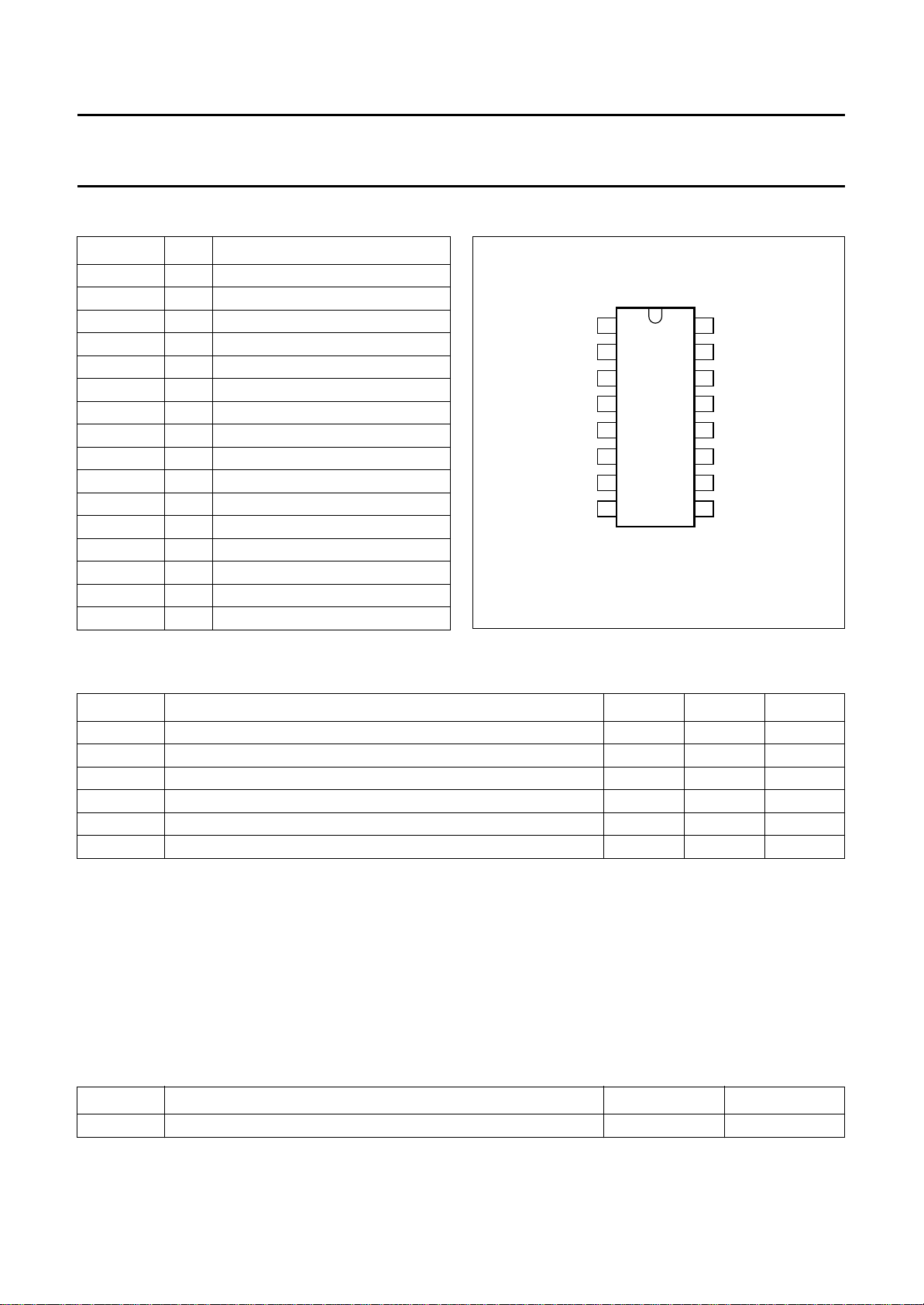
TDA5634T SO16
NAME DESCRIPTION VERSION
plastic small outline package; 16 leads; body width 3.9 mm
PACKAGE
SOT109-1
1996 Nov 7 2

Philips Semiconductors Product specification
9 V UHF mixer/oscillator for TV and VCR
tuners
BLOCK DIAGRAM
handbook, full pagewidth
UHF oscillator inputs
n.c.
UHF oscillator outputs
15 12 13 14
BCBC
UHF OSCILLATOR
MIXER
STABILIZER IF AMPLIFIER
V
P
11 10 916
TDA5634T
IF amplifier outputs
TDA5634T
RF STAGE
123456 78
RF
RF inputs local oscillator
GND
LOCAL
OSCILLATOR
outputs
GND
IF amplifier
inputs
Fig.1 Block diagram.
MBE299
1996 Nov 7 3
Philips Semiconductors Product specification
9 V UHF mixer/oscillator for TV and VCR
tuners
PINNING
SYMBOL PIN DESCRIPTION
CIN1 1 band C input 1
CIN2 2 band C input 2
RFGND 3 ground for RF inputs
LOOUT1 4 local oscillator amplifier output 1
LOOUT2 5 local oscillator amplifier output 2
GND 6 ground (0 V)
IFIN1 7 IF amplifier input 1
IFIN2 8 IF amplifier input 2
IFOUT1 9 IF amplifier output 1
IFOUT2 10 IF amplifier output 2
V
P
COSCIB1 12 UHF oscillator input base 1
COSCOC1 13 UHF oscillator output collector 1
COSCOC2 14 UHF oscillator output collector 2
COSCIB2 15 UHF oscillator input base 2
n.c. 16 not connected
11 supply voltage
handbook, halfpage
CIN1
1
2
CIN2
GND
IFIN1
IFIN2
3
4
TDA5634T
5
6
7
8
RFGND
LOOUT1
LOOUT2
Fig.2 Pin configuration.
MBE298
TDA5634T
n.c
16
COSCIB2
15
14
COSCOC2
13
COSCOC1
12
COSCIB1
V
11
P
10
IFOUT2
9
IFOUT1
LIMITING VALUES
In accordance with the Absolute Maximum Rating System (IEC 134).
SYMBOL PARAMETER MIN. MAX. UNIT
V
I
t
T
T
T
P
O
sc
stg
amb
j
supply voltage −0.3 +10.5 V
output current of each pin referenced to ground −−10 mA
maximum short-circuit time (all pins) − 10 s
IC storage temperature −55 +150 °C
operating ambient temperature −10 +80 °C
junction temperature − +150 °C
HANDLING
Human body model: the IC withstands 2000 V in accordance with the “
the
“MIL-STD-883C category B”
(2000 V);
UZW-BO/FQ-A302”
, specification equivalent to
R = 1500 Ω, C = 100 pF.
Machine model: the IC withstands 200 V except pin 11 (175 V) in accordance with the “
UZW-BO/FQ-B302”
, specification
(date of issue: Nov 6th, 1990);
R=0Ω, C = 200 pF.
THERMAL CHARACTERISTICS
SYMBOL PARAMETER VALUE UNIT
R
th j-a
thermal resistance from junction to ambient in free air 120 K/W
1996 Nov 7 4

Philips Semiconductors Product specification
9 V UHF mixer/oscillator for TV and VCR
TDA5634T
tuners
CHARACTERISTICS
=9V; T
V
P
SYMBOL PARAMETER CONDITIONS MIN. TYP. MAX. UNIT
Supply
V
P
I
P
Mixer (including IF amplifier)
f
RF
G
v
NF noise figure (not corrected
V
o
V
i
Z
i
=25°C; measured in circuit of Fig.7; unless otherwise specified.
amb
supply voltage 8.1 9.0 9.9 V
supply current VP= 8.1 to 9.9 V; T
= −10 to +80 °C − 35 45 mA
amb
RF frequency note 1 430 − 860 MHz
voltage gain fRF= 430 MHz; see Fig.3; note 2 33 36 39 dB
= 860 MHz; see Fig.3; note 2 33 36 39 dB
f
RF
= 430 MHz; see Fig.4 − 911dB
f
RF
for image)
output voltage causing 1%
cross modulation in channel
input voltage causing 10 kHz
= 860 MHz; see Fig.4 − 911dB
f
RF
fRF= 430 MHz; see Fig.5 115 118 − dBµV
= 860 MHz; see Fig.5 118 121 − dBµV
f
RF
fRF= 860 MHz; note 3 − 87 − dBµV
pulling in channel
input voltage causing
= 820 MHz; see Fig.6 65 72 − dBµV
f
RF
N+5−1 MHz pulling
input impedance (RS+jLSω)RS at fRF= 430 MHz; see Fig.8; note 4 − 28 −Ω
at fRF= 860 MHz; see Fig.8; note 4 − 33 −Ω
R
S
at fRF= 430 to 860 MHz; see Fig.8;
L
S
− 8 − nH
note 4
IF amplifier
S
11
S
12
S
21
S
22
Z
o
Y
i
input reflection coefficient magnitude; see Fig.10; note 4 −−0.6 − dB
phase; see Fig.10; note 4 −−2.5 − deg
reverse transmission
coefficient
forward transmission
coefficient
magnitude; see Fig.11; note 4 −−56 − dB
phase; see Fig.11; note 4 − 30 − deg
magnitude; note 4 −−9.5 − dB
phase; note 4 − 165 − deg
output reflection coefficient magnitude; see Fig.11; note 4 −−7−dB
phase; see Fig.11; note 4 − 6 − deg
output impedance
(RS+jLSω)
RS; see Fig.11; note 4 − 100 −Ω
; see Fig.11; note 4 − 32 − nH
L
S
input admittance (GP+jCPω)GP; see Fig.10; note 4 − 0.8 − mS
; see Fig.10; note 4 − 2.5 − pF
C
P
1996 Nov 7 5

Philips Semiconductors Product specification
9 V UHF mixer/oscillator for TV and VCR
TDA5634T
tuners
SYMBOL PARAMETER CONDITIONS MIN. TYP. MAX. UNIT
LO output; R
Y
o
V
o
SRF spurious signal on LO output
SHD LO signal harmonics with
Band C oscillator
f
OSC
f
shift
f
drift
= 100 Ω
L
output admittance
(GP+jCPω)
f
= 470 MHz; see Fig.9; note 4 − 3 − mS
OSC
− 0.5 − pF
f
= 900 MHz; see Fig.9; note 4 − 3.5 − mS
OSC
− 0.5 − pF
output voltage RL=50Ω; VP= 8.1 to 9.9 V;
T
= −10 to +80 °C
amb
R
=50Ω; note 5 −−−10 dBc
L
83 91 100 dBµV
with respect to LO output
signal
=50Ω −−−10 dBc
R
L
respect to LO signal
oscillator frequency Vt= 0.45 to 28 V; VP= 8.1 to 9.9 V;
T
= −10 to +80 °C; note 6
amb
470 − 900 MHz
frequency shift ∆VP= 10%; note 7 −−400 kHz
frequency drift ∆T=25°C without compensation;
−−2.5 MHz
NP0 capacitors; note 8
∆T=25°C with compensation; note 9 −−800 kHz
5 s to 15 minutes after switch on;
−−600 kHz
without compensation; note 10
Notes
1. The RF frequency range is defined by the oscillator frequency range and the intermediate frequency.
2. The gain is defined as the transducer gain (measured in Fig.7) plus the voltage transformation ratio of L3 to L2
(10 : 2, 15.4 dB including transformer loss).
3. The input level causing 10 kHz frequency detuning at the LO output; f
osc=fRF
+ 33.4 MHz.
4. All S-parameters are referred to a 50 Ω system.
5. Measured with RF input voltage of 97 dBµV at 430 MHz < fRF< 860 MHz.
6. Limits are related to the tank circuits used in Fig.7. Frequency bands may be adjusted by the choice of external
components.
7. The frequency shift is defined as the change in oscillator frequency when the supply voltage varies from
VP= 9 to 8.1 V or from VP= 9 to 9.9 V.
8. The frequency drift is defined as the change in oscillator frequency when the ambient temperature varies from
T
=25°C to 0 °C or from T
amb
=25°Cto50°C. Without compensation, the capacitors C11 to C15 are NP0.
amb
9. The frequency drift is defined as the change in oscillator frequency when the ambient temperature varies from
T
=25°C to 0 °C or from T
amb
=25°Cto50°C. With compensation, the capacitors C11 to C14 are N750 and
amb
C15 is N470.
10. Switch on drift is defined as the change in oscillator frequency between 5 s and 15 min after switch on.
1996 Nov 7 6
 Loading...