

Philips TDA5633T-C1, TDA5633M-C1, TDA5632M-C1, TDA5632M-C2 Datasheet

DATA SH EET
Product specification
Supersedes data of March 1995
File under Integrated Circuits, IC02
1996 Aug 16
INTEGRATED CIRCUITS
TDA5632; TDA5633
9 V VHF and UHF
mixers/oscillators for TV and VCR
cable tuners
1996 Aug 16 2
Philips Semiconductors Product specification
9 V VHF and UHF mixers/oscillators for
TV and VCR cable tuners
TDA5632; TDA5633
FEATURES
• Balanced mixer with a common emitter input for band A
• 2-pin oscillator for band A
• Balanced mixer with a common base input for band C
• 4-pin oscillator for band C
• Local oscillator buffer output for external prescaler
• SAW filter preamplifier with a low output impedance to
drive a 75 Ω load
• Band gap voltage stabilizer for oscillator stability
• Electronic band switch
• External IF filter connected between the mixer output
and the IF amplifier input.
APPLICATIONS
• Cable tuners for TV and VTR; switched concept for VHF
• Recommended RF bands for Europe:
48.25 to 105.25 MHz, 112.25 to 294.25 MHz and
471.25 to 855.25 MHz
• Recommended RF bands for the USA:
55.25 to 133.25 MHz, 139.25 to 361.25 MHz and
367.25 to 801.25 MHz.
DESCRIPTION
The TDA5632 and TDA5633 are monolithic integrated
circuits that perform VHF and UHF mixer/oscillator
functions in TV and VCR cable tuners. With correct
oscillator application and by using a switchable inductor to
split the VHF band into two sub-bands, the full VHF/UHF
TV bands can be covered. These low-power
mixers/oscillators require a power supply of 9 V and are
available in a very small package.
The devices provide the designer with the capability to
design an economical and physically small cable tuner.
The tuner development time can be drastically reduced by
using this device.
Frequency bands are determined by the external tank
circuit. They can be adapted to various standards.
QUICK REFERENCE DATA
Note
1. The limits are related to the tank circuits used in Fig.10 and the intermediate frequency. Frequency bands may be
adjusted by the choice of external components. Another UHF frequency range is available by modifying the tank
circuit. The modification enables the following frequency range:
a) RF frequencies from 361.25 to 801.25 MHz (picture carrier).
b) Oscillator frequencies from 407 to 847 MHz. For this UHF range, L4 = 3 turns (diameter = 3.5 mm).
SYMBOL PARAMETER CONDITIONS MIN. TYP. MAX. UNIT
V
P
supply voltage − 9.0 − V
I
P
supply current − 40 − mA
f
RF
frequency range (picture carrier) RF input; band A; note 1 57.5 − 357.5 MHz
RF input; band C; note 1 469.5 − 887.5 MHz
G
v
voltage gain band A (75 Ω load) − 19 − dB
band C (75 Ω load) − 30 − dB
NF noise figure band A (75 Ω load) − 10 − dB
band C (75 Ω load) − 9.5 − dB
V
o
output voltage to obtain 1% cross
modulation in channel
band A (75 Ω load) − 110 − dBµV
band C (75 Ω load) − 110 − dBµV

1996 Aug 16 3
Philips Semiconductors Product specification
9 V VHF and UHF mixers/oscillators for TV
and VCR cable tuners
TDA5632; TDA5633
ORDERING INFORMATION
BLOCK DIAGRAM
TYPE
NUMBER
PACKAGE
NAME DESCRIPTION VERSION
TDA5632T SO20
plastic small outline package; 20 leads; body width 7.5 mm
SOT163-1
TDA5632M SSOP20
plastic shrink small outline package; 20 leads; body width 4.4 mm
SOT266-1
TDA5633T SO20
plastic small outline package; 20 leads; body width 7.5 mm
SOT163-1
TDA5633M SSOP20
plastic shrink small outline package; 20 leads; body width 4.4 mm
SOT266-1
Fig.1 Block diagram.
The pin numbers in parenthesis represent the TDA5633.
handbook, full pagewidth
MBE269
BAND C
OSCILLATOR
4 (17) 5 (16) 6 (15) 7 (14)
COSCIB1
COSCIB2
BS IFOUT
COSCOC1
COSCOC2
BAND A
OSCILLATOR
1 (20) 3 (18)
AOSCIB AOSCOC
2 (19)
GND
band A oscillator
tuned circuit
band C oscillator
tuned circuit
MIXER MIXER
BAND A
STAGE
BAND C
STAGE
LOCAL
OSCILLATOR
AMPLIFIER
ELECTRONIC
BANDSWITCH
8 (13)
n.c.
9 (12)
band switch
input
DC
STABILIZER
IF
AMPLIFIER
10 (11)
IF output
15 (6) 14 (7) 13 (8) 12 (9) 11 (10)18 (3) 17 (4) 16 (5)
band C input
20 (1) 19 (2)
LOOUT2 LOOUT1
V
P
IFIN2 IFIN1CIN2 CIN1 RFGNDAIN2 AIN1
band A input
local oscillator
amplifier outputs
IF inputs
TDA5632
TDA5633
1996 Aug 16 4
Philips Semiconductors Product specification
9 V VHF and UHF mixers/oscillators for TV
and VCR cable tuners
TDA5632; TDA5633
PINNING
SYMBOL
PIN
DESCRIPTION
TDA5632 TDA5633
AOSCIB 1 20 band A oscillator input base
GND 2 19 ground (0 V)
AOSCOC 3 18 band A oscillator output collector
COSCIB1 4 17 band C oscillator input base 1
COSCOC1 5 16 band C oscillator output collector 1
COSCOC2 6 15 band C oscillator output collector 2
COSCIB2 7 14 band C oscillator input base 2
BS 8 13 band switch input
n.c. 9 12 not connected
IFOUT 10 11 IF amplifier output
IFIN1 11 10 IF amplifier input 1
IFIN2 12 9 IF amplifier input 2
V
P
13 8 supply voltage
LOOUT1 14 7 local oscillator amplifier output 1
LOOUT2 15 6 local oscillator amplifier output 2
RFGND 16 5 ground for RF inputs
CIN1 17 4 band C input 1
CIN2 18 3 band C input 2
AIN1 19 2 band A input 1
AIN2 20 1 band A input 2
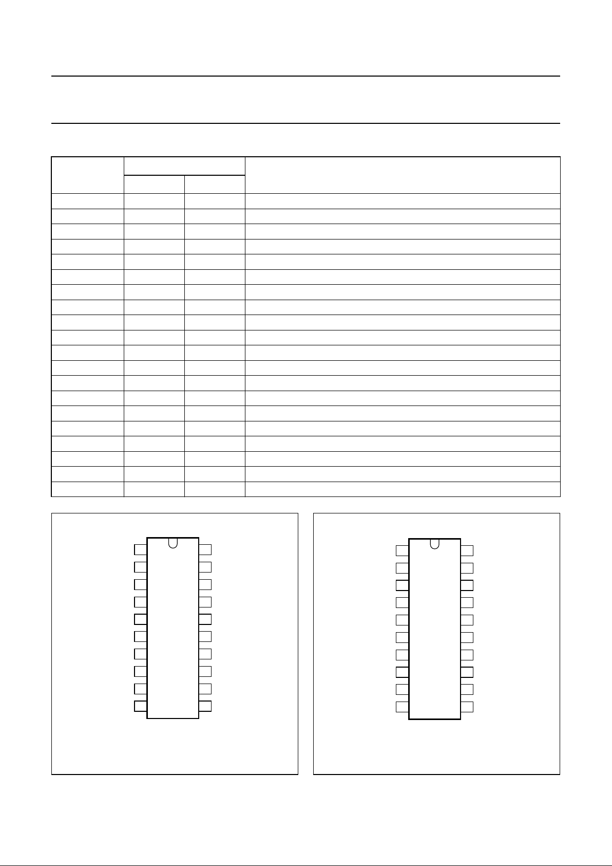
Fig.2 Pin configuration (TDA5632).
handbook, halfpage
TDA5632
MBE268
1
2
3
4
5
6
7
8
9
10
20
19
18
17
16
15
14
13
12
11
BS
V
IFOUT IFIN1
n.c. IFIN2
COSCIB2 LOOUT1
COSCOC2 LOOUT2
COSCOC1 RFGND
COSCIB1 CIN1
AOSCOC CIN2
GND AIN1
AOSCIB AIN2
P
Fig.3 Pin configuration (TDA5633).
handbook, halfpage
TDA5633
MBH328
1
2
3
4
5
6
7
8
9
10
20
19
18
17
16
15
14
13
12
11
V
P
BS
IFIN1 IFOUT
IFIN2 n.c.
LOOUT1 COSCIB2
LOOUT2 COSCOC2
RFGND COSCOC1
CIN1 COSCIB1
CIN2 AOSCOC
AIN1 GND
AIN2 AOSCIB

1996 Aug 16 5
Philips Semiconductors Product specification
9 V VHF and UHF mixers/oscillators for TV
and VCR cable tuners
TDA5632; TDA5633
LIMITING VALUES
In accordance with the Absolute Maximum Rating System (IEC 134).
THERMAL CHARACTERISTICS
HANDLING
Human body model: the IC withstands 2000 V in accordance with the
“UZW-B0/FQ-A302”
; specification equivalent to
the “
MIL-STD-883C, category B
”; R = 1.5 kΩ; C = 100 pF.
Machine model: the IC withstands 200 V in accordance with the
“UZW-B0/FQ-B302” (date of issue: Nov 6th, 1990)
;
R=0Ω; C = 200 pF.
IF AMPLIFIER CHARACTERISTICS
V
P
=9V; T
amb
=25°C; measured at 43.5 MHz; measured in circuit of Fig.10; unless otherwise specified.
SYMBOL PARAMETER MIN. MAX. UNIT
V
P
supply voltage −0.3 +10.5 V
V
SW
switching voltage 0 10.5 V
I
O
output current of each pin referenced to ground −−10 mA
t
sc
maximum short-circuit time (all pins) − 10 s
T
stg
IC storage temperature −55 +150 °C
T
amb
operating ambient temperature −20 +85 °C
T
j
junction temperature − +150 °C
SYMBOL PARAMETER VALUE UNIT
R
th j-a
thermal resistance from junction to ambient in free air
SOT163-1 80 K/W
SOT266-1 120 K/W
SYMBOL PARAMETER CONDITIONS MIN. TYP. MAX. UNIT
S
22
output reflection coefficient fIF= 43.5 MHz; see Fig.9 −−13.1 − dB
f
IF
= 43.5 MHz; see Fig.9 − 2.9 − deg
f
IF
= 58.75 MHz; see Fig.9 −−13.1 − dB
f
IF
= 58.75 MHz; see Fig.9 − 2.2 − deg
Z
O
output impedance fIF= 43.5 MHz; see Fig.9 − 78.4 −Ω
f
IF
= 43.5 MHz; see Fig.9 − 1.8 −Ω
f
IF
= 58.75 MHz; see Fig.9 − 78.4 −Ω
f
IF
= 58.75 MHz; see Fig.9 −−1.4 −Ω

1996 Aug 16 6
Philips Semiconductors Product specification
9 V VHF and UHF mixers/oscillators for TV
and VCR cable tuners
TDA5632; TDA5633
CHARACTERISTICS
V
P
=9V; T
amb
=25°C; measured in circuit of Fig.10; unless otherwise specified.
SYMBOL PARAMETER CONDITIONS MIN. TYP. MAX. UNIT
Supply
V
P
supply voltage 8.1 9.0 9.9 V
I
P
supply current − 40 48 mA
V
SW
switching voltage band A 0 − 2.0 V
band C 3.0 − 5.0 V
I
SW
switching current band A −−2µA
band C −−10 µA
Band A mixer including IF amplifier
f
RF
frequency range note 1 57.5 − 357.5 MHz
G
v
voltage gain fRF= 57.5 MHz; RL=75Ω; see Fig.4 16.5 19 21.5 dB
f
RF
= 357.5 MHz; RL=75Ω; see Fig.4 16.5 19 21.5 dB
NF noise figure f
RF
= 50 MHz; RL=75Ω; see Fig.5 − 7.5 9.5 dB
f
RF
= 150 MHz; RL=75Ω; see Fig.5 − 8.5 10.5 dB
f
RF
= 300 MHz; RL=75Ω−10 12.5 dB
V
o
output voltage causing 1%
cross modulation in channel
fRF= 57.5 MHz; RL=75Ω; see Fig.6 107 110 − dBµV
f
RF
= 357.5 MHz; RL=75Ω; see Fig.6 107 110 − dBµV
V
i
input voltage causing 10 kHz
pulling in channel
fRF= 357.5 MHz; RL=75Ω; see note 2 − 91 − dBµV
g
os
optimum source
conductance for noise figure
fRF= 50 MHz; RL=75Ω−0.5 − mS
f
RF
= 150 MHz; RL=75Ω−1.1 − mS
f
RF
= 300 MHz; RL=75Ω−1.9 − mS
g
i
input conductance fRF= 57.5 MHz − 0.27 − mS
f
RF
= 357.5 MHz − 0.68 − mS
C
i
input capacitance fRF= 57.5 to 357.5 MHz; RL=75Ω−2−pF
Band A oscillator
f
osc
frequency range note 3 101 − 401 MHz
f
shift
frequency shift ∆VP= 10%; note 4 −−200 kHz
f
drift
frequency drift ∆T=25°C with no compensation;
NP0 capacitors; note 5
−−1200 kHz
5 s to 15 min after switch on; note 6 −−400 kHz
 Loading...