

Page 1

TDA5051A
Home automation modem
Rev. 5 — 13 January 2011 Product data sheet
1. General description
The TDA5051A is a modem IC, specifically dedicated to ASK transmission by means of
the home power supply network, at 600 baud or 1200 baud data rate. It operates from a
single 5 V supply.
2. Features and benefits
Full digital carrier generation and shaping
Modulation/demodulation frequency set by clock adjustment, from microcontroller or
on-chip oscillator
High clock rate of 6-bit D/A (Digital to Analog) converter for rejection of aliasing
components
Fully integrated output power stage with overload protection
Automatic Gain Control (AGC) at receiver input
8-bit A/D (Analog to Digital) converter and narrow digital filtering
Digital demodulation delivering baseband data
Easy compliance with EN50065-1 with simple coupling network
Few external components for low cost applications
SO16 plastic package
3. Applications
Home appliance control (air conditioning, shutters, lighting, alarms and so on)
Energy/heating control
Amplitude Shift Keying (ASK) data transmission using the home power network
Page 2

NXP Semiconductors
4. Quick reference data
TDA5051A
Home automation modem
Table 1. Quick reference data
Symbol Parameter Conditions Min Typ Max Unit
V
DD
I
DD(tot)
supply voltage 4.75 5.0 5.25 V
total supply current f
=8.48MHz
osc
Reception mode - 28 38 mA
[1]
Transmission mode;
DATA_IN
=0; ZL=30Ω
-4768mA
Power-down mode - 19 25 mA
f
f
V
V
cr
osc
o(rms)
i(rms)
carrier frequency
oscillator frequency 6.08 - 9.504 MHz
output carrier signal (RMS value) DATA_IN = LOW;
input signal (RMS value)
THD total harmonic distortion on CISPR16 load
= CISPR16
Z
L
[2]
- 132.5 - kHz
120 - 122 dBμV
[3]
82 - 122 dBμV
- −55 - dB
with coupling network
T
amb
[1] The value of the total transmission mode current is the sum of I
[2] Frequency range corresponding to the EN50065-1 band. However, the modem can operate at any lower oscillator frequency.
[3] The minimum value can be improved by using an external amplifier; see application diagrams Figure 19
ambient temperature −50 - +100 °C
DD(RX/TX)(tot)
+ I
in the Table 5 “Characteristics”.
DD(PAMP)
and Figure 20.
5. Ordering information
Table 2. Ordering information
Type number Package
TDA5051AT SO16 plastic small outline package; 16 leads; body width 7.5 mm SOT162-1
Name Description Version
TDA5051A All information provided in this document is subject to legal disclaimers. © NXP B.V. 2011. All rights reserved.
Product data sheet Rev. 5 — 13 January 2011 2 of 29
Page 3
NXP Semiconductors
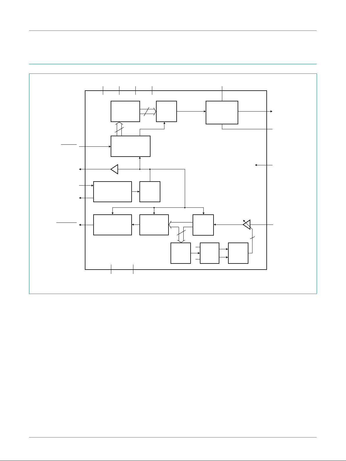
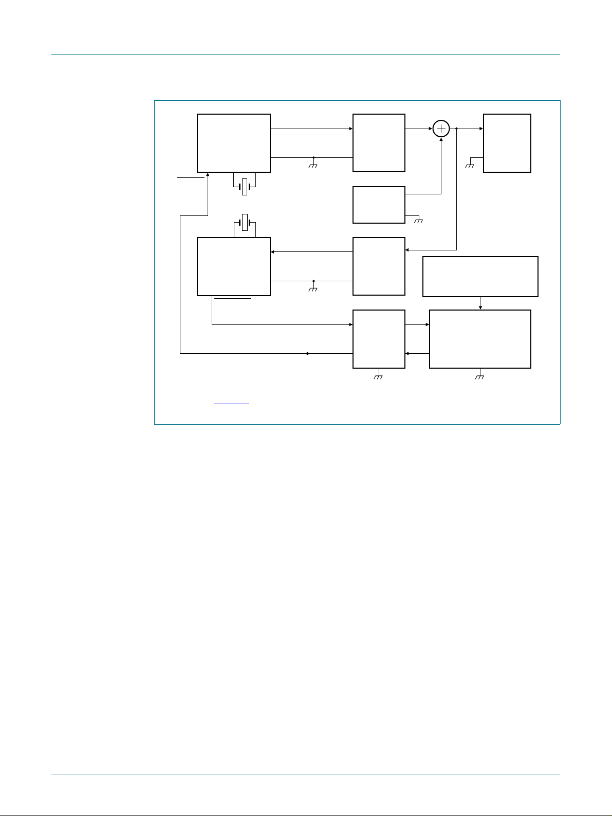
6. Block diagram
TDA5051A
Home automation modem
DATA_IN
CLK_OUT
OSC1
OSC2
DATA_OUT
DGND5AGND12V
1
4
7
OSCILLATOR
8
2
DIGITAL
DEMODULATOR
TEST1 SCANTEST
DDA
13
ROM
10
CONTROL LOGIC
16
6
V
DDD
311
6
D/A
DAC clock
modulated
carrier
V
DDAP
POWER
DRIVE
WITH
PROTECTION
10
9
TDA5051A
filter clock
÷ 2
DIGITAL
BAND-PASS
FILTER
8
PEAK
DETECT
A/D
H
L
U
U/D
D
COUNT
15
14
5
002aaf038
TX_OUT
APGND
PD
RX_IN
Fig 1. Block diagram
TDA5051A All information provided in this document is subject to legal disclaimers. © NXP B.V. 2011. All rights reserved.
Product data sheet Rev. 5 — 13 January 2011 3 of 29
Page 4
NXP Semiconductors
7. Pinning information
7.1 Pinning
TDA5051A
Home automation modem
DATA_IN TEST1
DATA_OUT PD
CLK_OUT V
SCANTEST V
1
2
3
V
DDD
4
TDA5051AT
5
DGND AGND
6
7
OSC1 TX_OUT
8
OSC2 APGND
Fig 2. Pin configuration for SO16
7.2 Pin description
Table 3. Pin description
Symbol Pin Description
DATA_IN
DATA_OUT
V
DDD
CLK_OUT 4 clock output
DGND 5 digital ground
SCANTEST 6 test input (LOW in application)
OSC1 7 oscillator input
OSC2 8 oscillator output
APGND 9 analog ground for power amplifier
TX_OUT 10 analog signal output
V
DDAP
AGND 12 analog ground
V
DDA
RX_IN 14 analog signal input
PD 15 power-down input (active HIGH)
TEST1 16 test input (HIGH in application)
1 digital data input (active LOW)
2 digital data ou tput (active LOW)
3 digital supply voltage
11 analog supply voltage for power amplifier
13 analog supply voltage
002aaf039
16
15
14
RX_IN
13
DDA
12
11
DDAP
10
9
TDA5051A All information provided in this document is subject to legal disclaimers. © NXP B.V. 2011. All rights reserved.
Product data sheet Rev. 5 — 13 January 2011 4 of 29
Page 5

NXP Semiconductors
8. Functional description
Both transmission and reception stages are controlled either by the master clock of the
microcontroller or by the on-chip reference oscillator connected to a crystal. This ensures
the accuracy of the transmission carrier and the exact trimming of the digital filter, thus
making the performance totally independent of application disturbances such as
component spread, temperature, supply drift and so on.
TDA5051A
Home automation modem
The interface with the power network is made by means of an LC network (see Figure 15
The device includes a power output stage that feeds a 120 dBμV (RMS) signal on a
typical 30 Ω load.
To reduce power consumption, the IC is disabled by a power-down input (pin PD): in this
mode, the on-chip oscillator remains active and the clock continues to be supplied at
pin CLK_OUT. For low-power operation in reception mode, this pin can be dynamically
controlled by the microcontroller, see Section 8.4 “
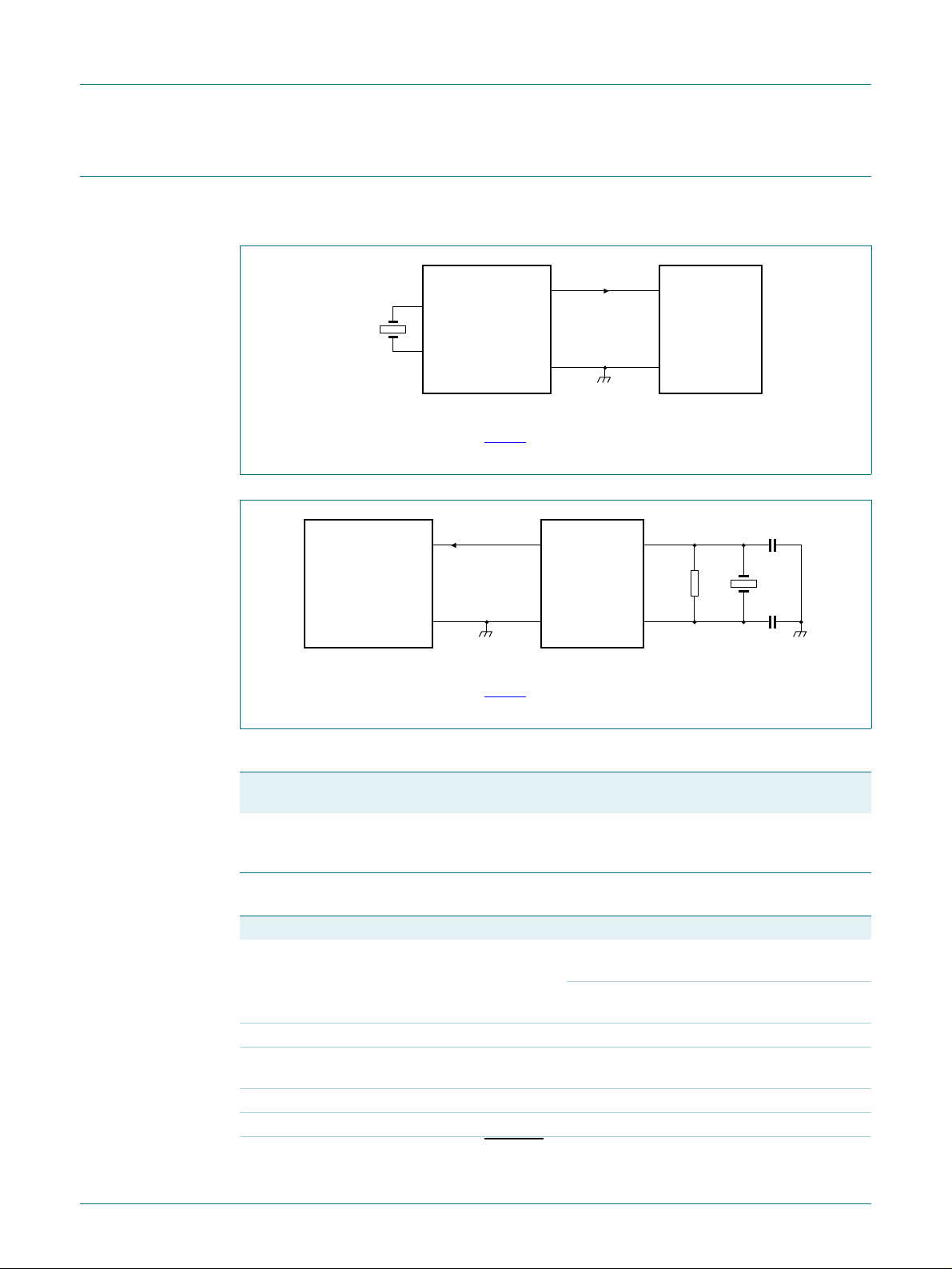
When the circuit is connected to an external clock generator (see Figure 6
signal must be applied at pin OSC1 (pin 7); OSC2 (pin 8) must be left open-circuit.
Figure 7
All logic inputs and outputs are compatible with TTL/CMOS levels, providing an easy
connection to a standard microcontroller I/O port.
The digital part of the IC is fully scan-testable. Two digital inputs, SCANTEST and TEST1,
are used for production test: these pins must be left open-circuit in functional mode
(correct levels are internally defined by pull-up or pull-down resistors).
shows the use of the on-chip clock circuit.
Power-down mode”.
), the clock
8.1 Transmission mode
To provide strict stability with respect to environmental conditions, the carrier frequency is
generated by scanning the ROM memory under t he con trol of the microcon troller clock or
the reference frequency provided by the on-chip oscillator. High frequency clocking rejects
the aliasing components to such an extent that they are filtered by the coupling
LC network and do not cause any significant disturbance. The data modulation is applied
through pin DATA_IN
(shaping). Harmonic components are limited in this process, thus avoiding unaccep table
disturbance of the transmission channel (according to CISPR16 and EN50065-1
recommendations). A −55 dB Tot al Harmonic Distortion ( THD) is reached when the typical
LC coupling network (or an equivalent filter) is used.
and smoothly applied by specific digital circuits to the carrier
).
The DAC and the power stage are set in order to provide a maximum signal level of
122 dBμV (RMS) at the output.
The output of the power stage (TX_OUT) must always be connected to a decoup ling
capacitor, because of a DC level of 0.5V
device is not transmitting. This pin must also be protected against overvoltage and
negative transient signals. The DC level of TX_OUT can be used to bias a unipolar
transient suppressor, as shown in the application diagram (see Figure 15
Direct connection to the mains is done through an LC network for low-cost applications.
However, an HF signal transformer could be used when power-line insulation has to be
performed.
TDA5051A All information provided in this document is subject to legal disclaimers. © NXP B.V. 2011. All rights reserved.
Product data sheet Rev. 5 — 13 January 2011 5 of 29
at this pin, which is present even when the
DD
).
Page 6

NXP Semiconductors
Remark: In transmission mode, the receiving part of the circuit is not disabled and the
detection of the transmitted signal is normally performed. In this mode, the gain chosen
before the beginning of the transmission is stored, and the AGC is internally set to
−6dB as long as DATA_IN
8.2 Reception mode
The input signal received by the modem is applied to a wide range input amplifier with
AGC (−6 dB to +30 dB). This is basically for noise performance improvement and signal
level adjustment, which ensures a maximum sensitivity of the ADC. An 8-bit conversion is
then performed, followed by digital band-pass filtering, to meet the CISPR16
normalization and to comply with some additional limitations met in current applications.
After digital demodulation, the baseband data signal is made available after pulse
shaping.
The signal pin (RX_IN) is a high-impedance input which has to be protected and
DC decoupled for the same reasons as with pin TX_OUT. The high sensitivity (82 dBμV)
of this input requires an efficient 50 Hz rejection filter (realized by the LC coupling
network), which also acts as an anti-aliasing filter for the internal digital processing;
(see Figure 15
TDA5051A
Home automation modem
is LOW. Then, the old gain setting is automatically restored.
).
8.3 Data format
8.3.1 Transmission mode
The data input (DATA_IN) is active LOW: this means that a burst is generated on the line
(pin TX_OUT) when DATA_IN
Pin TX_OUT is in a high-impedance state as long as the device is not transmitting.
Successive logic 1s are treated in a Non-Return-to-Zero (NRZ) mode, see pulse shapes
in Figure 8
and Figure 9.
8.3.2 Reception mode
The data output (pin DATA_OUT) is active LOW; this means that the data output is LOW
when a burst is received. Pin DATA_OUT
8.4 Power-down mode
Power-down input (pin PD) is active HIGH; this means that the power consumption is
minimum when pin PD is HIGH. Now, all functions are disabled, except clock generation.
pin is LOW.
remains LOW as long as a burst is received.
TDA5051A All information provided in this document is subject to legal disclaimers. © NXP B.V. 2011. All rights reserved.
Product data sheet Rev. 5 — 13 January 2011 6 of 29
Page 7

NXP Semiconductors
9. Limiting values
Table 4. Limiting values
In accordance with the Absolute Maximum Rating System (IEC 60134).
Symbol Parameter Conditions Min Max Unit
V
DD
f
osc
T
stg
T
amb
T
j
10. Characteristics
TDA5051A
Home automation modem
supply voltage 4.5 5.5 V
oscillator frequency - 12 MHz
storage temperature −50 +150 °C
ambient temperature −50 +100 °C
junction temperature - 125 °C
Table 5. Characteristics
V
DDD=VDDA
=5V±5%; T
=−40°C to +85°C; V
amb
connected to V
DDD
; DGND connected to AGND.
DDA
Symbol Parameter Conditions Min Typ Max Unit
Supply
V
DD
I
DD(tot)
supply voltage 4.75 5 5.25 V
total supply current f
=8.48MHz
osc
Reception mode - 28 38 mA
[1]
Transmission
-4768mA
mode;
DATA_IN
=0;
ZL=30Ω
Power-down mode - 19 25 mA
I
DD(RX/TX)(tot)
total analog + digital
supply current
VDD=5V± 5%;
Transmission or
-2838mA
Reception mode
I
DD(PD)(tot)
total analog + digital
supply current
VDD=5V± 5%;
PD = HIGH;
-1925mA
Power-down mode
I
DD(PAMP)
power amplifier
supply current
VDD=5V± 5%;
=30Ω;
Z
L
DATA_IN
= LOW in
-1930mA
Transmission mode
I
DD(PAMP)(max)
maximum power amplifier
supply current
VDD=5V± 5%;
=1Ω;
Z
L
DATA_IN
= LOW in
-76-mA
Transmission mode
DATA_IN
V
IH
V
IL
V
OH
V
OL
and PD inputs; DATA_OUT and CLK_OUT outputs
HIGH-level input voltage 0.2VDD+0.9 - VDD+0.5 V
LOW-level input voltage −0.5 - 0.2VDD− 0.1 V
HIGH-level output voltage IOH= −1.6 mA 2.4 - - V
LOW-level output voltage IOL= 1.6 mA - - 0.45 V
TDA5051A All information provided in this document is subject to legal disclaimers. © NXP B.V. 2011. All rights reserved.
Product data sheet Rev. 5 — 13 January 2011 7 of 29
Page 8

NXP Semiconductors
TDA5051A
Home automation modem
Table 5. Characteristics …continued
V
DDD=VDDA
Symbol Parameter Conditions Min Typ Max Unit
OSC1 input and OSC2 output (OSC2 only used for driving external quartz crystal; must be left open-circuit when
using an external clock generator)
V
IH
V
IL
V
OH
V
OL
Clock
f
osc
f
osc/fcr
f
osc/fCLKOUT
Transmission mode
f
cr
t
su
t
h
t
W(DI)(min)
V
o(rms)
I
o(max)
Z
o
V
O
THD total harmonic distortion on
B
−20dB
=5V±5%; T
HIGH-level input voltage 0.7V
=−40°C to +85°C; V
amb
connected to V
DDD
; DGND connected to AGND.
DDA
DD
-V
+0.5 V
DD
LOW-level input voltage −0.5 - 0.2VDD− 0.1 V
HIGH-level output voltage IOH= −1.6 mA 2.4 - - V
LOW-level output voltage IOL= 1.6 mA - - 0.45 V
oscillator frequency 6.080 - 9.504 MHz
ratio between oscillator and
-64-
carrier frequency
ratio between oscillator and
-2-
clock output frequency
carrier frequency f
set-up time of the shaped
burst
hold time of the shaped
burst
minimum pulse width of
DATA_IN
signal
output carrier signal
(RMS value)
power amplifier maximum
output current (peak value)
output impedance of the
=8.48MHz
osc
f
= 8.48 MHz;
osc
see Figure 8
f
= 8.48 MHz;
osc
see Figure 8
f
= 8.48 MHz;
osc
see Figure 8
DATA_IN = LOW;
ZL= CISPR16
DATA_IN = LOW;
=1Ω
Z
L
[2]
- 132.5 - kHz
- 170 - μs
- 170 - μs
- 190 - μs
120 - 122 dBμV
- 160 - mA
-5-Ω
power amplifier
output DC level at
-2.5-V
pin TX_OUT
CISPR16 load with the
coupling network (measured
on the first ten harmonics)
= 121 dBμV on
V
o(rms)
CISPR16 load;
= 8.48 MHz;
f
osc
DATA_IN
=LOW
- −55 - dB
(no modulation);
see Figure 3
and
Figure 22
bandwidth of the shaped
output signal (at −20 dB)
on CISPR16 load with the
coupling network
V
= 121 dBμV on
o(rms)
CISPR16 load;
= 8.48 MHz;
f
osc
DATA_IN = 300 Hz;
- 3000 - Hz
duty factor = 50 %;
see Figure 4
TDA5051A All information provided in this document is subject to legal disclaimers. © NXP B.V. 2011. All rights reserved.
Product data sheet Rev. 5 — 13 January 2011 8 of 29
Page 9

NXP Semiconductors
TDA5051A
Home automation modem
Table 5. Characteristics
V
DDD=VDDA
=5V±5%; T
…continued
=−40°C to +85°C; V
amb
connected to V
DDD
; DGND connected to AGND.
DDA
Symbol Parameter Conditions Min Typ Max Unit
Reception mode
V
i(rms)
analog input signal
[3]
82 - 122 dBμV
(RMS value)
V
I
Z
i
R
AGC
t
c(AGC)
DC level at pin RX_IN - 2.5 - V
RX_IN input impedance - 50 - kΩ
AGC range - 36 - dB
AGC time constant f
= 8.48 MHz;
osc
- 296 - μs
see Figure 5
t
d(dem)(su)
demodulation delay
set-up time
t
d(dem)(h)
demodulation delay
hold time
B
det
detection bandwidth f
BER bit error rate f
f
= 8.48 MHz;
osc
- 350 400 μs
see Figure 21
f
= 8.48 MHz;
osc
- 420 470 μs
see Figure 21
=8.48MHz-3-kHz
osc
= 8.48 MHz;
osc
-1-1× 10
600 baud;
S/N = 35 dB;
signal 76 dBμV;
see Figure 23
Power-up timing
t
d(pu)(TX)
delay between power-up
and DATA_IN
in
transmission mode
XTAL = 8.48 MHz;
C1 = C2 = 27 pF;
Rp=2.2MΩ;
-1-μs
see Figure 10
t
d(pu)(RX)
delay between power-up
and DATA_OUT in
reception mode
XTAL = 8.48 MHz;
C1 = C2 = 27 pF;
Rp=2.2MΩ;
= 132.5 kHz;
f
RXIN
-1-μs
120 dBμV sine wave;
see Figure 11
Power-down timing
t
d(pd)(TX)
delay between PD = 0 and
DATA_IN
in transmission
f
= 8.48 MHz;
osc
see Figure 12
-10-μs
mode
t
d(pd)(RX)
delay between PD = 0 and
DATA_OUT
in reception
mode
= 8.48 MHz;
f
osc
f
= 132.5 kHz;
RXIN
120 dBμV sine wave;
- 500 - μs
see Figure 13
t
active(min)
minimum active time with
T = 10 ms power-down
period in reception mode
f
= 8.48 MHz;
osc
f
= 132.5 kHz;
RXIN
120 dBμV sine wave;
-1-μs
see Figure 14
−4
[1] The value of the total transmission mode current is the sum of I
[2] Frequency range corresponding to the EN50065-1 band. However, the modem can operate at any lower oscillator frequency.
[3] The minimum value can be improved by using an external amplifier; see application diagrams Figure 19
TDA5051A All information provided in this document is subject to legal disclaimers. © NXP B.V. 2011. All rights reserved.
Product data sheet Rev. 5 — 13 January 2011 9 of 29
DD(RX/TX)(tot)
+ I
DD(PAMP)
.
and Figure 20.
Page 10

NXP Semiconductors
002aaf054
8
TDA5051A
Home automation modem
0
V
o(rms)
(dBV)
−20
−40
−60
−80
−100
5
10
Resolution bandwidth = 9 kHz; top: 0 dBV (RMS) = 120 dBμV (RMS); marker at
−5dBV(RMS)=115dBμV (RMS); the CISPR16 network provides an attenuation of 6 dB,
so the signal amplitude is 121 dBμV (RMS).
Fig 3. Carrier spectrum
−10
dBV
(RMS)
−20
−30
132.5 kHz
1500 Hz
20 dB
f (Hz)
002aaf057
6
10
−40
−50
−60
117.5 147.5
Resolution bandwidth = 100 Hz; B
Fig 4. Shaped signal spectrum
V
RXIN
V
(I)
0
G
AGC
+30 dB
−6 dB
(AGC time constant)
132.5
= 3000 Hz (2 × 1500 Hz).
−20dB
modulated sine wave 122 dBμV amplitude
t
c(AGC)
8.68 dB
f (kHz)
t
AGC range
002aaf05
Fig 5. AGC time constant definition (not to scale)
TDA5051A All information provided in this document is subject to legal disclaimers. © NXP B.V. 2011. All rights reserved.
Product data sheet Rev. 5 — 13 January 2011 10 of 29
Page 11
NXP Semiconductors
2
3
11. Timing
11.1 Configuration for clock
Fig 6. External clock
CLK_OUT
XTAL
MICROCONTROLLER
For parameter description, see Table 6.
GND
TDA5051A
Home automation modem
OSC1
DGND
7
TDA5051A
5
002aaf04
f
osc
CLK_OUT
MICROCONTROLLER
GND
CLK_OUT
1
/2 f
osc
DGND
4
TDA5051A
5
8
7
OSC2
OSC1
R
p
C1
XTAL
C2
002aaf04
For parameter description, see Table 6.
Fig 7. Typical configuration for on-chip clock circuit
Table 6. Clock oscillator parameters
Oscillator
frequency f
6.080 MHz to
9.504 MHz
osc
Carrier
frequency f
95 kHz to
148.5 kHz
Clock output frequency
1
cr
⁄
2fosc
External components
3.040 MHz to 4.752 MHz C1 = C2 = 27 pF to 47 pF;
R
=2.2MΩ to 4.7 MΩ;
p
XTAL= standard quartz crystal
Table 7. Calculation of parameters depending on the clock frequency
Symbol Parameter Conditions Unit
f
osc
oscillator frequency with on-chip oscillator: frequency of
Hz
the crystal quartz
with external clock: frequency of the
Hz
signal applied at OSC1
f
CLKOUT
f
cr
clock output frequency
carrier frequency/digital filter tuning
1
⁄
2fosc
1
⁄
64fosc
Hz
Hz
frequency
t
su
t
h
t
W(DI)(min)
set-up time of the shaped burst 23/fcr or 1472/f
hold time of the shaped burst 23/fcr or 1472/f
minimum pulse width of DATA_IN
tsu + 1/f
cr
osc
osc
s
s
s
signal
TDA5051A All information provided in this document is subject to legal disclaimers. © NXP B.V. 2011. All rights reserved.
Product data sheet Rev. 5 — 13 January 2011 11 of 29
Page 12

NXP Semiconductors
4
5
TDA5051A
Home automation modem
Table 7. Calculation of parameters depending on the clock frequency
…continued
Symbol Parameter Conditions Unit
t
W(burst)(min)
t
c(AGC)
t
su(demod)
t
h(demod)
minimum burst time of V
O(DC)
signal t
W(DI)(min)
AGC time constant 2514/f
demodulation set-up time 3200/f
demodulation hold time 3800/f
t
TX_OUT
V
O(DC)
DATA_IN
t
W(burst)
t
0
su
t
W(DI)
(1) (2) (3)
W(burst)(min)
t
h
t
W(DI)(min)
+ t
h
osc
(max.) s
osc
(≈max.) s
osc
002aaf04
s
s
(1) t
W(DI)>tW(DI)(min)
(2) t
W(DI)(min)=tsu
(3) t
W(DI)(min)<tsu
+1/f
cr
; wrong operation
Fig 8. Relationship between DATA_IN and TX_OUT (see Table 8)
T able 8. Relationship between DATA_IN
and TX_OUT
X = don’t care.
PD DATA_IN TX_OUT
1 X high-impedance
0 1 high-impedance (after t
)
h
0 0 active with DC offset
t
W(burst)
100 %
t
su
t
h
002aaf04
Fig 9. Pulse shape characteristics
TDA5051A All information provided in this document is subject to legal disclaimers. © NXP B.V. 2011. All rights reserved.
Product data sheet Rev. 5 — 13 January 2011 12 of 29
Page 13

NXP Semiconductors
6
7
8
1 1.2 Timing diagrams
V
90 % V
DD
TDA5051A
Home automation modem
DD
CLK_OUT
DATA_IN
TX_OUT
(1)
not defined clock stable
HIGH
t
d(pu)(TX)
(1) DATA_IN is an edge-sensitive input and must be HIGH before starting a transmission.
Fig 10. Timing diagram during power-up in Transmission mode
90 % V
V
DD
CLK_OUT
RX_IN
DATA_OUT
DD
not defined
not defined
t
d(pu)(RX)
clock stable
HIGH
t
d(dem)(h)
002aaf04
002aaf04
Fig 11. Timing diagram during power-up in Reception mode
PD
DATA_IN
TX_OUT
t
d(pd)(TX)
normal operation wrong operation
TX_OUT
delayed by PD
002aaf04
Fig 12. Power-down sequence in Transmission mode
TDA5051A All information provided in this document is subject to legal disclaimers. © NXP B.V. 2011. All rights reserved.
Product data sheet Rev. 5 — 13 January 2011 13 of 29
Page 14

NXP Semiconductors
9
0
TDA5051A
Home automation modem
PD
RX_IN
DATA_OUT
t
d(dem)(su)
DATA_OUT delayed by PD
t
d(pd)(RX)
Fig 13. Power-down sequence in Reception mode
PD
RX_IN
DATA_OUT
t
active(min)
I
DD(RX)
I
DD
I
DD(PD)
0
T
Fig 14. Power saving by dynamic control of power-down
t
d(pd)(RX)
002aaf04
002aaf05
TDA5051A All information provided in this document is subject to legal disclaimers. © NXP B.V. 2011. All rights reserved.
Product data sheet Rev. 5 — 13 January 2011 14 of 29
Page 15
NXP Semiconductors
12. Application information
TDA5051A
Home automation modem
+5 V
250 V (AC)
MICRO-
CONTROLLER
max
+5 V
DATA_IN
DATA_OUT
CLK_OUT
47 nF
78L05
2
PD
T 630 mA
31
1
2
4
15
7
OSC1
7.3728 MHz
470 μF
(16 V)
2.2 MΩ
XTAL
MOV
250 V (AC)
U
1N4006
7V5
(1.3 W)
100 μF
(16 V)
V
DDDVDDAP
3
TDA5051A
85 9 12
OSC2
27 pF27 pF
APGND
2 μF
250 V (AC)
68 Ω
(2 W)
1 mH
1N4006
V
DDA
1311
14
10
AGNDDGND
RX_IN
TX_OUT
47 nF
(63 V)
47 μH
10 nF
SA5.0A
47 nF/X2
250 V (AC)
47 μH
low R
1 μF
(16 V)
002aaf059
S
fcr = 115.2kHz for XTAL = 7.3728 MHz standard crystal.
Fig 15. Application diagram without power line insulation
TDA5051A All information provided in this document is subject to legal disclaimers. © NXP B.V. 2011. All rights reserved.
Product data sheet Rev. 5 — 13 January 2011 15 of 29
Page 16
NXP Semiconductors
002aaf055
TDA5051A
Home automation modem
20
G
(dB)
−20
−60
−100
10 10
2
10
3
10
4
10
5
10
a. Gain
3
10
Z
i
(Ω)
2
10
10
10 10
2
10
3
10
4
10
5
10
b. Input impedance
fcr= 115.2 kHz; L = 47 μH; C = 47 nF.
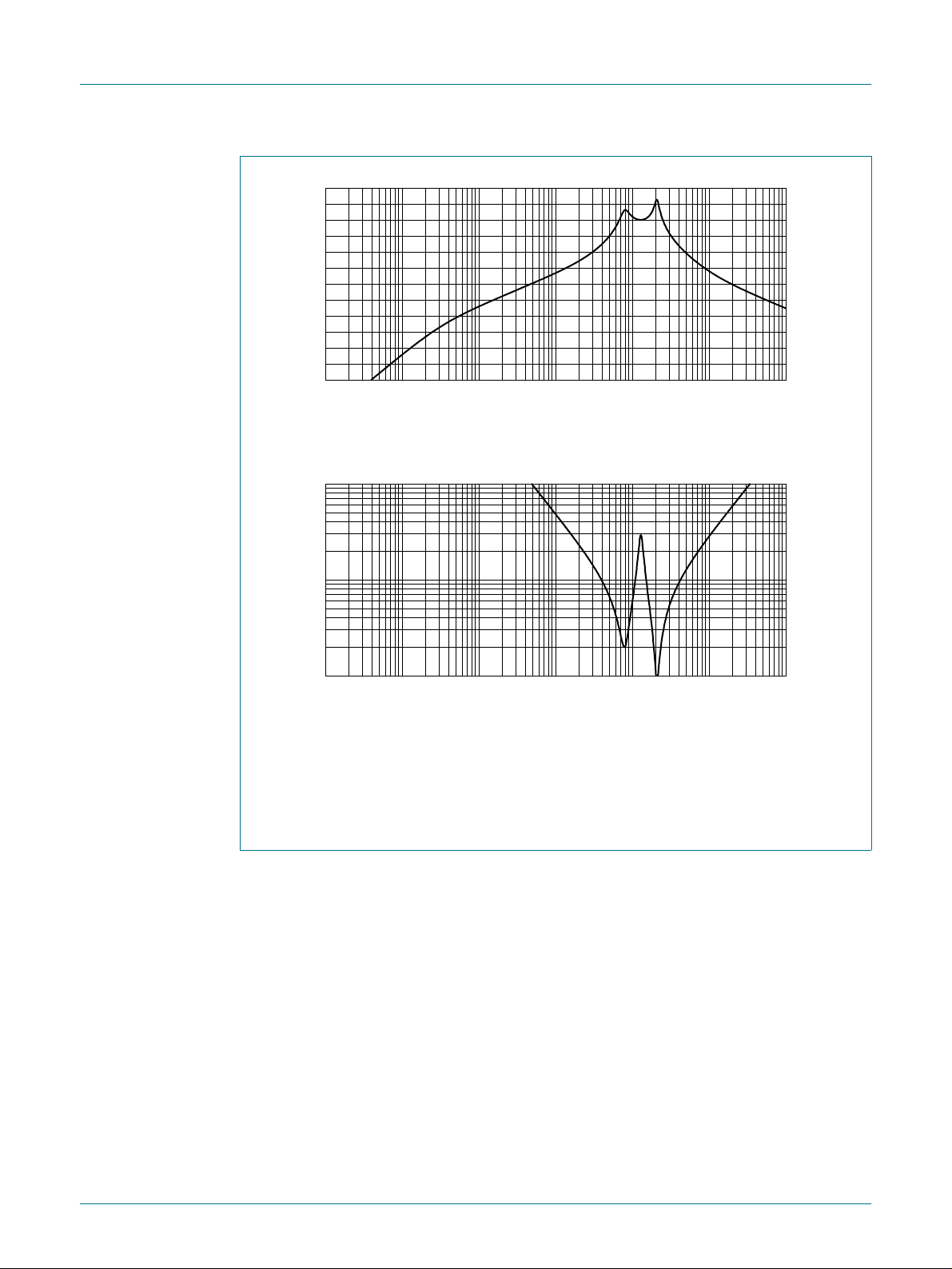
Main features of the coupling network: 50 Hz rejection > 80 dB; anti-aliasing for the digital filter >
50 dB at the sampling frequency (
1
⁄
). Input impedance always higher than 10 Ω within the
2fosc
95 kHz to 148.5 kHz band.
Fig 16. Gain (a) and input impedance (b) of the coupling network
6
10
f (Hz)
002aaf431
6
10
f (Hz)
7
7
TDA5051A All information provided in this document is subject to legal disclaimers. © NXP B.V. 2011. All rights reserved.
Product data sheet Rev. 5 — 13 January 2011 16 of 29
Page 17
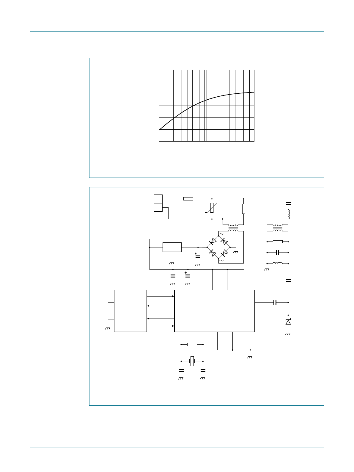
NXP Semiconductors
002aaf056
130
V
o
(dBμV)
120
110
TDA5051A
Home automation modem
100
110
10
with coupling network; L = 47 μH; C = 47 nF.
Fig 17. Output voltag e as a function of line impedance
+5 V
250 V (AC)
MICRO-
CONTROLLER
max
+5 V
47 nF
DATA_IN
DATA_OUT
CLK_OUT
78L05
2
PD
1
2
4
15
T 630 mA
7
31
470 μF
(16 V)
100 μF
(16 V)
OSC1
2.2 MΩ
XTAL
7.3728 MHz
MOV
250 V (AC)
U
1 VA
+
FDB08
V
DDDVDDAP
3
TDA5051A
85 9 12
OSC2
1311
100 Ω
(0.5 W)
V
DDA
14
10
2
RX_IN
TX_OUT
AGNDDGND
1
2
Newport/
Murata
78250
100 Ω
100 nF
(63 V)
22 μH
10 nF
SA5.0A
470 nF/X2
250 V (AC)
47 μH
low R
6
5
1 μF
(16 V)
S
Z
(Ω)
line
230 V
6 V
−
APGND
27 pF27 pF
002aaf060
fcr= 115.2 kHz for XTAL = 7.3728 MHz standard crystal.
Fig 18. Application diagram with power line insulation
TDA5051A All information provided in this document is subject to legal disclaimers. © NXP B.V. 2011. All rights reserved.
Product data sheet Rev. 5 — 13 January 2011 17 of 29
Page 18
NXP Semiconductors
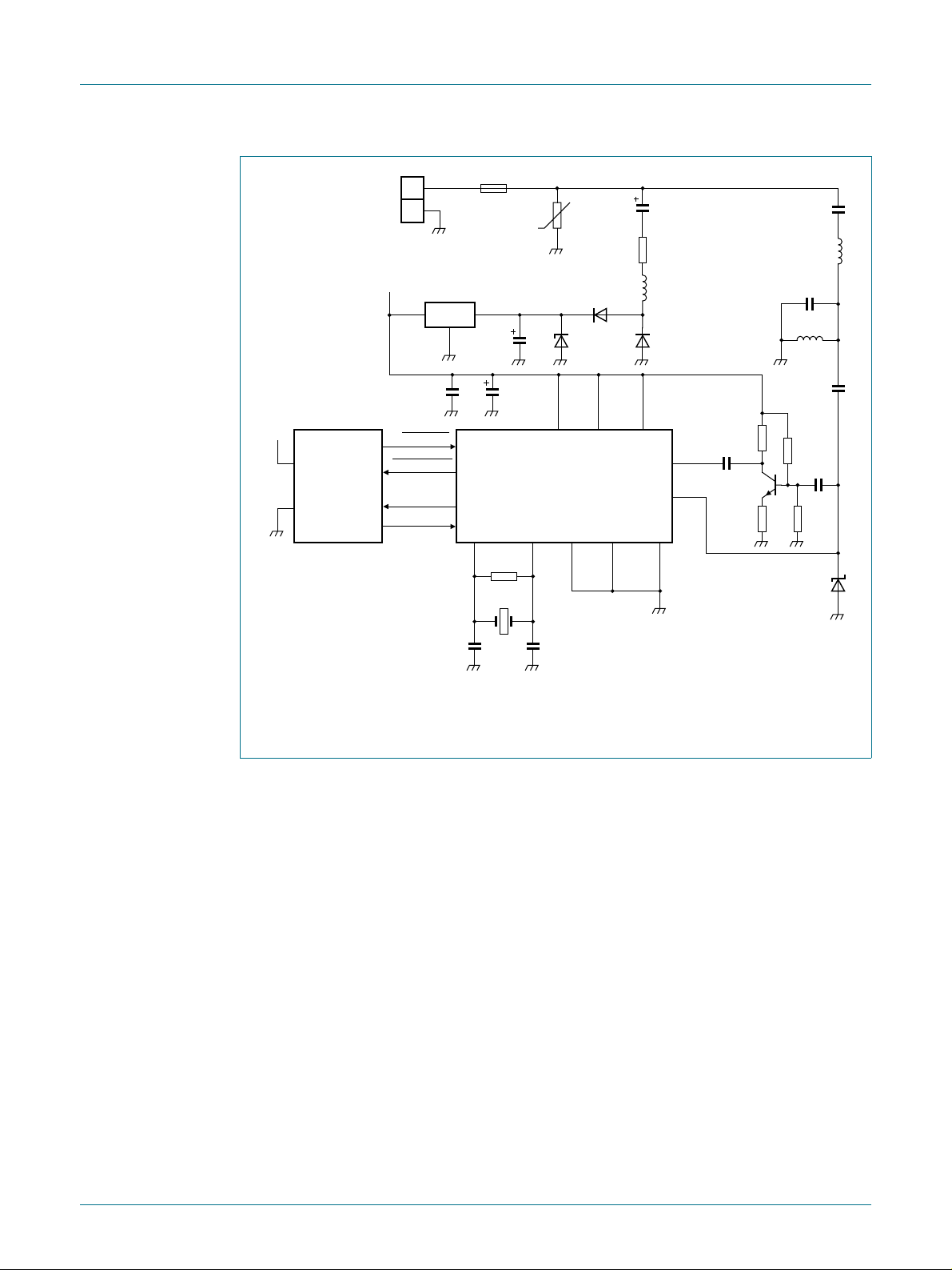
61
TDA5051A
Home automation modem
+5 V
250 V (AC)
MICRO-
CONTROLLER
max
+5 V
DATA_IN
DATA_OUT
CLK_OUT
47 nF
78L05
2
PD
T 630 mA
31
1
2
4
15
7
OSC1
7.3728 MHz
470 μF
(16 V)
2.2 MΩ
XTAL
MOV
250 V (AC)
U
1N4006
7V5
(1.3 W)
100 μF
(16 V)
V
DDDVDDAP
3
TDA5051A
85 9 12
OSC2
27 pF27 pF
APGND
2 μF
250 V (AC)
68 Ω
(2 W)
1 mH
1N4006
V
DDA
1311
14
10
AGNDDGND
RX_IN
TX_OUT
10 nF
10 kΩ
BC547B
1 kΩ
47 nF/X2
250 V (AC)
47 μH
low R
47 nF
(63 V)
47 μH
1 μF
(16 V)
150 kΩ
10 nF
33 kΩ
SA5.0A
002aaf0
S
fcr= 115.2 kHz for XTAL = 7.3728 MHz standard crystal.
Fig 19. Application diagram without power line insulation, with impro ved sensit ivit y
(68 dBμV typ.)
TDA5051A All information provided in this document is subject to legal disclaimers. © NXP B.V. 2011. All rights reserved.
Product data sheet Rev. 5 — 13 January 2011 18 of 29
Page 19

NXP Semiconductors
TDA5051A
Home automation modem
+5 V
250 V (AC)
MICRO-
CONTROLLER
max
+5 V
DATA_IN
DATA_OUT
CLK_OUT
47 nF
78L05
2
PD
1
2
4
15
T 630 mA
7
31
470 μF
(16 V)
100 μF
(16 V)
OSC1
2.2 MΩ
XTAL
7.3728 MHz
230 V
6 V
−
1311
100 Ω
(0.5 W)
V
DDA
14
10
RX_IN
TX_OUT
MOV
250 V (AC)
U
1 VA
+
FDB08
V
DDDVDDAP
3
TDA5051A
85 9 12
OSC2
27 pF27 pF
APGND
AGNDDGND
10 nF
10 kΩ
BC547B
1 kΩ
470 nF/X2
250 V (AC)
Newport/
Murata
78250
1
2
100 Ω
100 nF
(63 V)
22 μH
150 kΩ
SA5.0A
1 μF
(16 V)
10 nF
33 kΩ
002aaf062
47 μH
low R
6
5
S
fcr= 115.2 kHz for XTAL = 7.3728 MHz standard crystal.
Fig 20. Application diagram with power line insulation, with improved sensitivity
(68 dBμV typ.)
TDA5051A All information provided in this document is subject to legal disclaimers. © NXP B.V. 2011. All rights reserved.
Product data sheet Rev. 5 — 13 January 2011 19 of 29
Page 20
NXP Semiconductors
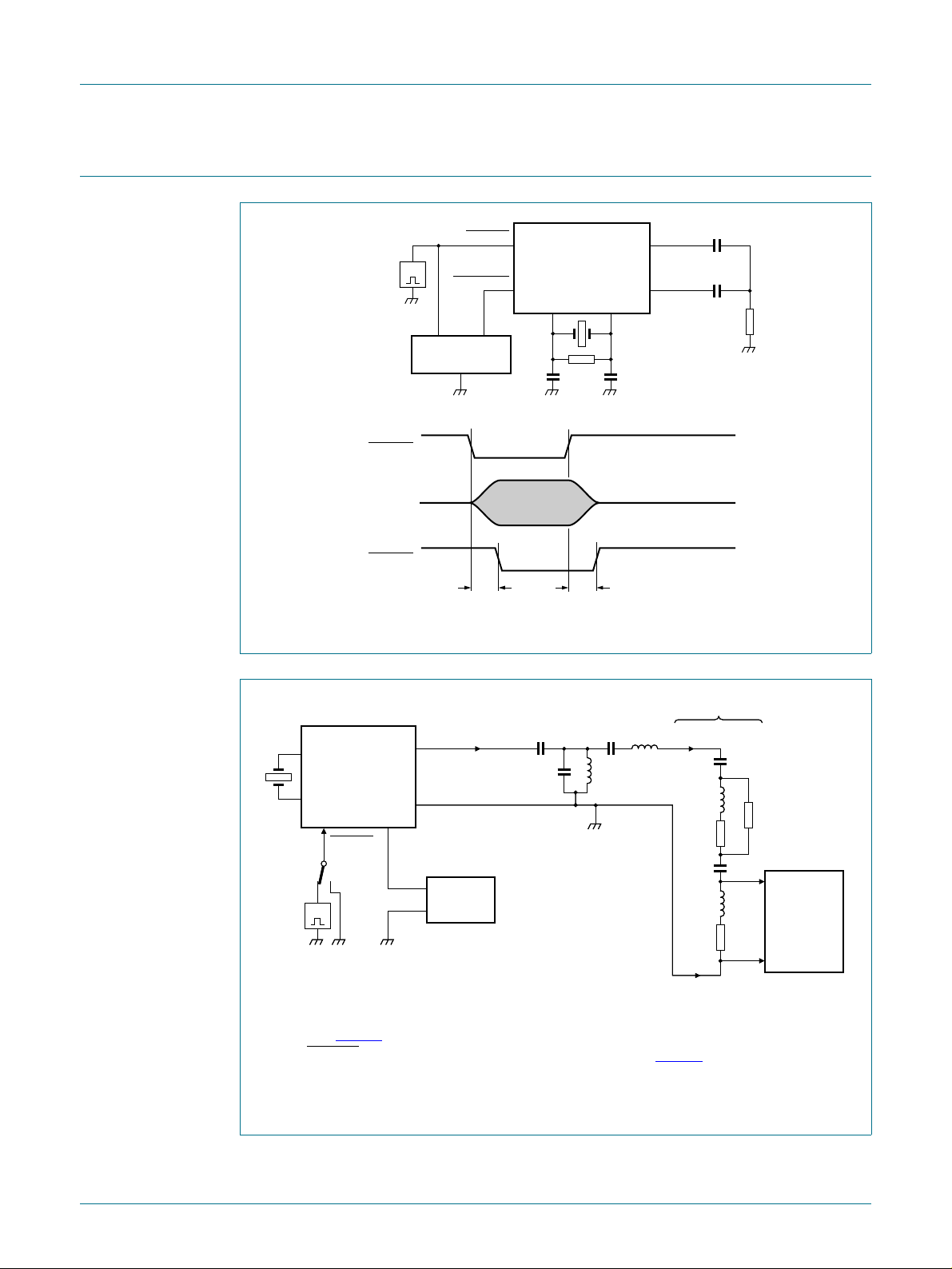
2
2
13. Test information
TDA5051A
Home automation modem
pulse
generator
300 Hz
50 %
DATA_IN
G
DATA_OUT
1
TDA5051A
(to be tested)
2
78
Y1
Y2
OSCILLOSCOPE
DATA_IN
TX_OUT/RX_IN
DATA_OUT
t
d(dem)(su)
t
d(dem)(h)
Fig 21. Test set-up for measuring demodulation delay
XTAL
f
osc
10
14
TX_OUT
RX_IN
1 μF
10 nF
30 Ω
002aaf051
(3)
OSC1
OSC1
OSC2
OSC2
7
7
TDA5051A
TDA5051A
8
8
1 13, 3, 11
1 13, 3, 11
DATA_IN
DATA_IN
(2)(1)
(2)(1)
G
G
TX_OUT
TX_OUT
10
10
AGND, DGND, APGND
AGND, DGND, APGND
12, 5, 9
12, 5, 9
V
V
, V
, V
DDA
DDA
+5 V
+5 V
, V
, V
DDD
DDD
POWER
POWER
SUPPLY
SUPPLY
DDAP
DDAP
coupling network
coupling network
10 μF
10 μF
33 nF
33 nF
33 nF
33 nF
47 μH
47 μH
(3)
47 μH
47 μH
CISPR16 network
CISPR16 network
250 nF
250 nF
50 μH
50 μH
5 Ω
5 Ω
250 nF
250 nF
50 μH
50 μH
5 Ω
5 Ω
50 Ω
50 Ω
(1) Square wave TTL signal 300 Hz, duty factor = 50 % for measuring signal bandwidth
(see Figure 3
(2) DATA_IN
(3) Tuned for f
).
+ LOW for measuring total harmonic distortion (see Figure 3).
= 132.5 kHz.
cr
(4) The CISPR16 network provides a −6 dB attenuation.
Fig 22. Test set-up for measuring THD and bandwidth of the TX_OUT signal
(4)
(4)
SPECTRUM
SPECTRUM
ANALYZER
ANALYZER
50 Ω
50 Ω
002aaf05
002aaf05
TDA5051A All information provided in this document is subject to legal disclaimers. © NXP B.V. 2011. All rights reserved.
Product data sheet Rev. 5 — 13 January 2011 20 of 29
Page 21
NXP Semiconductors
TDA5051A
Home automation modem
DATA_IN
TDA5051A
78
1
OSC1 OSC2
XTAL = 8.48 MHz
OSC1 OSC2
78
TDA5051A
(to be tested)
2
DATA_OUT
TX_OUT
10
AGND, DGND, APGND
12,
5,
9
RX_IN
14
12,
AGND, DGND, APGND
5,
9
out
DATA_IN
DATA_OUT
in
COUPLING
NETWORK
WHITE
NOISE
GENERATOR
COUPLING
NETWORK
V24/TTL
INTERFACE
(1) See Figure 22.
Fig 23. Test set-up for measuring Bit Error Rate (BER)
+
out
(1)
(1)
+
out
in
PSEUDO RANDOM SEQUENCE:
2
RXD
V24 SERIAL DATA
TXD
SPECTRUM
ANALYZER
PARAMETERS
600 BAUD
9
−1 BITS LONG
ANALYZER
50 Ω
002aaf053
TDA5051A All information provided in this document is subject to legal disclaimers. © NXP B.V. 2011. All rights reserved.
Product data sheet Rev. 5 — 13 January 2011 21 of 29
Page 22

NXP Semiconductors
S
-1
14. Package outline
TDA5051A
Home automation modem
O16: plastic small outline package; 16 leads; body width 7.5 mm
16
1
y
Z
pin 1 index
D
c
9
A
2
A
1
8
e
w M
b
p
E
H
E
detail X
A
X
v M
Q
(A )
L
p
L
A
3
θ
SOT162
A
0 5 10 mm
scale
DIMENSIONS (inch dimensions are derived from the original mm dimensions)
mm
OUTLINE
VERSION
SOT162-1
A
A1A2A3b
max.
0.3
2.65
0.1
0.012
0.1
0.004
p
2.45
2.25
0.096
0.089
IEC JEDEC JEITA
075E03 MS-013
0.25
0.01
0.49
0.36
0.019
0.014
0.32
0.23
0.013
0.009
UNIT
inches
Note
1. Plastic or metal protrusions of 0.15 mm (0.006 inch) maximum per side are not included.
(1)E(1) (1)
cD
10.5
10.1
0.41
0.40
REFERENCES
eHELLpQ
7.6
7.4
0.30
0.29
1.27
0.05
10.65
10.00
0.419
0.394
1.4
0.055
1.1
0.4
0.043
0.016
1.1
1.0
0.043
0.039
0.25
0.25 0.1
0.01
0.01
EUROPEAN
PROJECTION
ywv θ
Z
0.9
0.4
0.035
0.004
0.016
ISSUE DATE
99-12-27
03-02-19
o
8
o
0
Fig 24. Package outline SOT162-1 (SO16)
TDA5051A All information provided in this document is subject to legal disclaimers. © NXP B.V. 2011. All rights reserved.
Product data sheet Rev. 5 — 13 January 2011 22 of 29
Page 23

NXP Semiconductors
15. Handling information
All input and output pins are protected against ElectroS tatic Discharge (ESD) under
normal handling. When handling ensure that the appropriate precautions are taken as
described in JESD625-A or equivalent standards.
16. Soldering of SMD packages
This text provides a very brief insight into a complex technology. A more in-depth account
of soldering ICs can be found in Application Note AN10365 “Surface mount reflow
soldering description”.
16.1 Introduction to soldering
Soldering is one of the most common methods through which packages are attached to
Printed Circuit Boards (PCBs), to form electrical circuits. The soldered joint provides both
the mechanical and the electrical connection. There is no single soldering method that is
ideal for all IC packages. Wave soldering is often preferred when through-hole and
Surface Mount Devices (SMDs) are mixed on one printed wiring board; however, it is not
suitable for fine pitch SMDs. Reflow soldering is ideal for the small pitches and high
densities that come with increased miniaturization.
TDA5051A
Home automation modem
16.2 Wave and reflow soldering
Wave soldering is a joining technology in which the joints are made by so lder coming from
a standing wave of liquid solder. The wave soldering process is suitable for the following:
• Through-hole components
• Leaded or leadless SMDs, which are glued to the surface of the printed circuit board
Not all SMDs can be wave soldered. Packages with solder balls, and some leadless
packages which have solder lands underneath the body, cannot be wave soldered. Also,
leaded SMDs with leads having a pitch smaller than ~0.6 mm cannot be wave soldered,
due to an increased probability of bridging.
The reflow soldering process involves applying solder paste to a board, followed by
component placement and exposure to a temperature profile. Leaded packages,
packages with solder balls, and leadless packages are all reflow solderable.
Key characteristics in both wave and reflow soldering are:
• Board specifications, including the board finish, solder masks and vias
• Package footprints, including solder thieves and orientation
• The moisture sensitivity level of the packages
• Package placement
• Inspection and repair
• Lead-free soldering versus SnPb soldering
16.3 Wave soldering
Key characteristics in wave soldering are:
TDA5051A All information provided in this document is subject to legal disclaimers. © NXP B.V. 2011. All rights reserved.
Product data sheet Rev. 5 — 13 January 2011 23 of 29
Page 24

NXP Semiconductors
• Process issues, such as application of adhesive and flux, clinching of leads, board
• Solder bath specifications, including temperature and impurities
16.4 Reflow soldering
Key characteristics in reflow soldering are:
• Lead-free versus SnPb soldering; note that a lead-free reflow process usually lea ds to
• Solder paste printing issues including smearing, release, and adjusting the process
• Reflow temperature profile; this profile includes preheat, reflow (in which the board is
Table 9. SnPb eutectic process (from J-STD-020C)
Package thickness (mm) Package reflow temperature (°C)
< 2.5 235 220
≥ 2.5 220 220
TDA5051A
Home automation modem
transport, the solder wave parameters, and the time during which components are
exposed to the wave
higher minimum peak temperatures (see Figure 25
reducing the process window
window for a mix of large and small components on one board
heated to the peak temperature) and cooling down. It is imperative that the peak
temperature is high enough for the solder to make reliable solder joint s (a solder paste
characteristic). In addition, the peak temperature must be low enough that the
packages and/or boards are not damaged. The peak temperature of the package
depends on package thickness and volume and is classified in accordance with
Table 9
and 10
Volume (mm3)
< 350 ≥ 350
) than a SnPb process, thus
Table 10. Lead-free process (from J-STD-020C)
Package thickness (mm) Package reflow temperature (°C)
Volume (mm3)
< 350 350 to 2000 > 2000
< 1.6 260 260 260
1.6 to 2.5 260 250 245
> 2.5 250 245 245
Moisture sensitivity precautions, as indicated on the packing, must be respected at all
times.
Studies have shown that small packages reach higher temperatures during reflow
soldering, see Figure 25
TDA5051A All information provided in this document is subject to legal disclaimers. © NXP B.V. 2011. All rights reserved.
Product data sheet Rev. 5 — 13 January 2011 24 of 29
.
Page 25
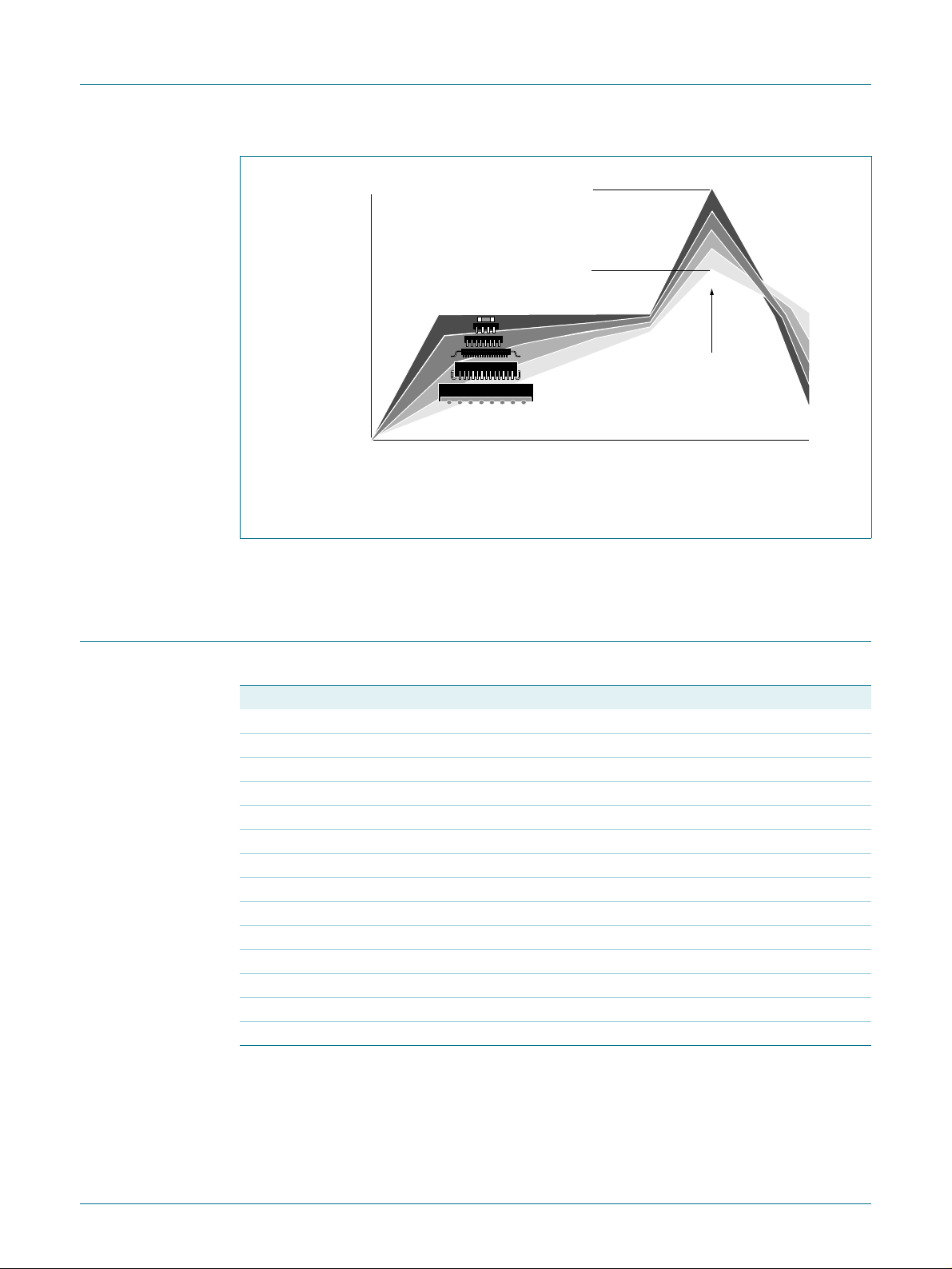
NXP Semiconductors
4
Fig 25. Temperature profiles for large and small components
maximum peak temperature
temperature
MSL: Moisture Sensitivity Level
= MSL limit, damage level
minimum peak temperature
= minimum soldering temperature
TDA5051A
Home automation modem
peak
temperature
time
001aac84
For further information on temperature profiles, refer to Application Note AN10365
“Surface mount reflow soldering description”.
17. Abbreviations
Table 11. Abbreviations
Acronym Description
ADC Analog-to-Digital Converter
AGC Automatic Gain Control
ASK Amplitude Shift Keying
CMOS Complementary Metal-Oxide Semiconductor
DAC Di gital-to-Analog Con v erter
HF High-Frequency
I/O Input/Output
IC Integrated Circuit
LC inductor-capacitor filter
NRZ Non-Return-to-Zero
RMS Root Mean Squared
ROM Read-Only Memory
THD Total Harmonic Distortion
TTL Transistor-Transistor Logic
TDA5051A All information provided in this document is subject to legal disclaimers. © NXP B.V. 2011. All rights reserved.
Product data sheet Rev. 5 — 13 January 2011 25 of 29
Page 26

NXP Semiconductors
TDA5051A
Home automation modem
18. Revision history
Table 12. Revision history
Document ID Release date Data sheet status Change notice Supersedes
TDA5051A v.5 20110113 Product data sheet - TDA5051A v.4
Modifications:
• Table 1 “Quick reference data”, T
– Min value changed from −10 °C to −50 °C
– Max value changed from +80 °C to +100 °C
• Table 4 “Limiting values”, T
– Min value changed from −10 °C to −50 °C
– Max value changed from +80 °C to +100 °C
amb
• Table 5 “Characteristics”, descriptive line below title is changed from “T
to “T
TDA5051A v.4 20100701 Product data sheet - TDA5051A v.3
TDA5051A v.3 20100422 Preliminary data sheet - TDA5051A v.2
TDA5051A v.2
(9397 750 05035)
TDA5051A v.1
(9397 750 02571)
19990531 Product specification - TDA5051A v.1
19970919 Product specification - -
= −40 °C to +85 °C”
amb
, ambient temperature:
amb
, ambient temperature:
=0°C to 70 °C”
amb
TDA5051A All information provided in this document is subject to legal disclaimers. © NXP B.V. 2011. All rights reserved.
Product data sheet Rev. 5 — 13 January 2011 26 of 29
Page 27

NXP Semiconductors
TDA5051A
Home automation modem
19. Legal information
19.1 Data sheet status
Document status
Objective [short] data sheet Development This document contains data from the objective specification for product development.
Preliminary [short] data sheet Qualification This document contains data from the preliminary specification.
Product [short] data sheet Production This document contains the product specification.
[1] Please consult the most recently issued document before initiating or completing a design.
[2] The term ‘short data sheet’ is explained in section “Definitions”.
[3] The product status of device(s) d escribed i n this docume nt may have changed since this docume nt was publis hed and ma y dif fer in case of multiple devices. The latest product status
information is available on the Internet at URL http://www.nxp.com.
[1][2]
Product status
[3]
Definition
19.2 Definitions
Draft — The document is a draft version only. The content is still under
internal review and subject to formal approval, which may result in
modifications or additions. NXP Semiconductors does not give any
representations or warranties as to the accuracy or completeness of
information included herein and shall have no liability for the consequences of
use of such information.
Short data sheet — A short data sheet is an extract from a full data sheet
with the same product type number(s) and title. A short data sheet is intended
for quick reference only and should not be relied u pon to co nt ain det ailed and
full information. For detailed and full information see the relevant full data
sheet, which is available on request via the local NXP Semiconductors sales
office. In case of any inconsistency or conflict with the short data sheet, the
full data sheet shall prevail.
Product specification — The information and data provided in a Product
data sheet shall define the specification of the product as agreed between
NXP Semiconductors and its customer, unless NXP Semiconductors and
customer have explicitly agreed otherwise in writing. In no event however,
shall an agreement be valid in which the NXP Semiconductors product is
deemed to offer functions and qualities beyond those described in the
Product data sheet.
19.3 Disclaimers
Limited warranty and liability — Information in this document is believed to
be accurate and reliable. However, NXP Semiconductors does not give any
representations or warranties, expressed or implied, as to the accuracy or
completeness of such information and shall have no liability for the
consequences of use of such information.
In no event shall NXP Semiconductors be lia ble for any indirect, incidental,
punitive, special or consequential damages (including - without limitation - lost
profits, lost savings, business interruption, costs related to the removal or
replacement of any products or rework charges) whether or not such
damages are based on tort (including negligence), warranty, breach of
contract or any other legal theory.
Notwithstanding any damages that customer might incur for any reason
whatsoever, NXP Semi conductors’ aggregat e and cumulative liabil ity towards
customer for the products described herein shall be limited in accordance
with the Terms and conditions of commercial sale of NXP Semiconductors.
Right to make changes — NXP Semiconductors reserves the right to make
changes to information published in this document, including without
limitation specifications and product descriptions, at any time and without
notice. This document supersedes and replaces all information supplied prior
to the publication hereof.
Suitability for use — NXP Semiconductors products are not designed,
authorized or warranted to be suitable for use in life support, life-critical or
safety-critical systems or equipment, nor in applications where failure or
malfunction of an NXP Semiconductors product can reasonabl y be expected
to result in personal injury, death or severe property or environmental
damage. NXP Semiconductors accepts no liability for inclusion and/or use of
NXP Semiconductors products in such equipment or applications and
therefore such inclusion and/or use is at the customer’s own risk.
Applications — Applications that are described herein for any of these
products are for illustrative purposes only. NXP Semiconductors makes no
representation or warranty that such applications will be suitable for the
specified use without further testing or modification.
Customers are responsible for the design and operation of their applications
and products using NXP Semiconductors products, and NXP Semiconductors
accepts no liability for any assistance with applications or customer product
design. It is customer’s sole responsibility to determine whether the NXP
Semiconductors product is suitable and fit for the customer’s applications and
products planned, as well as for the planned application and use of
customer’s third party customer(s). Customers should provide appropriate
design and operating safeguards to minimize the risks associated with their
applications and products.
NXP Semiconductors does not accept any liability related to any default ,
damage, costs or problem which is based on any weakness or default in the
customer’s applications or products, or the application or use by customer’s
third party customer(s). Customer is responsible for doing all necessary
testing for the customer’s applications and products using NXP
Semiconductors products in order to avoid a default of the applications and
the products or of the application or use by customer’s third part y
customer(s). NXP does not accept any liability in this respect.
Limiting values — Stress above one or more limiting values (as defined in
the Absolute Maximum Ratings System of IEC 60134) will cause permanent
damage to the device. Limiting values are stress ratings only and (proper)
operation of the device at these or any other conditions above those given in
the Recommended operating conditions section (if present) or the
Characteristics sections of this document is not warranted. Constant or
repeated exposure to limiting values will permanently and irreversibly affect
the quality and reliability of the device.
Terms and conditions of commercial sale — NXP Semiconductors
products are sold subject to the general terms and conditions of commercial
sale, as published at http://www.nxp.com/profile/terms
agreed in a valid written individual agreement. In case an individual
agreement is concluded only the terms and conditions of the respective
agreement shall apply. NXP Semiconductors hereby expressly objects to
applying the customer’s general terms and conditions with regard to the
purchase of NXP Semiconductors products by customer.
No offer to sell or license — Nothing in this document may be interpreted or
construed as an offer to sell product s that is ope n for accept ance or the gr ant,
conveyance or implication of any license under any copyrights, patents or
other industrial or intellectual property rights.
Export control — This document as well as the item(s) described herein
may be subject to export control regulations. Export might require a prior
authorization from national authorities.
, unless otherwise
TDA5051A All information provided in this document is subject to legal disclaimers. © NXP B.V. 2011. All rights reserved.
Product data sheet Rev. 5 — 13 January 2011 27 of 29
Page 28

NXP Semiconductors
TDA5051A
Home automation modem
Quick reference data — The Quick reference data is an extract of the
product data given in the Limiting values and Characteristics sections of this
document, and as such is not complete, exhaustive or legally binding.
Non-automotive qualified products — Unless this data sheet expressly
states that this specific NXP Semiconductors product is automotive qualified,
the product is not suitable for automotive use. It i s neither qua lif ied nor test ed
in accordance with automotive testing or application requirements. NXP
Semiconductors accepts no liability for inclusion and/or use of
non-automotive qualified products in automotive equ ipment or applications.
In the event that customer uses the product for design-in and use in
automotive applications to automotive specifications and standards, customer
(a) shall use the product without NXP Semiconductors’ warranty of the
product for such automotive applications, use and specifications, and (b)
whenever customer uses the product for automotive applications beyond
NXP Semiconductors’ specifications such use shall be solely at customer’s
own risk, and (c) customer fully indemnifies NXP Semiconductors for any
liability, da mages or failed produ ct cl aims resulting from custome r design and
use of the product for automotive applications beyond NXP Semiconductors’
standard warranty and NXP Semiconductors’ product specifications.
19.4 Trademarks
Notice: All referenced brands, prod uct names, service names and trad emarks
are the property of their respective owners.
20. Contact information
For more information, please visit: http://www.nxp.com
For sales office addresses, please send an email to: salesaddresses@nxp.com
TDA5051A All information provided in this document is subject to legal disclaimers. © NXP B.V. 2011. All rights reserved.
Product data sheet Rev. 5 — 13 January 2011 28 of 29
Page 29

NXP Semiconductors
21. Contents
1 General description. . . . . . . . . . . . . . . . . . . . . . 1
2 Features and benefits . . . . . . . . . . . . . . . . . . . . 1
3 Applications. . . . . . . . . . . . . . . . . . . . . . . . . . . . 1
4 Quick reference data . . . . . . . . . . . . . . . . . . . . . 2
5 Ordering information. . . . . . . . . . . . . . . . . . . . . 2
6 Block diagram . . . . . . . . . . . . . . . . . . . . . . . . . . 3
7 Pinning information. . . . . . . . . . . . . . . . . . . . . . 4
7.1 Pinning . . . . . . . . . . . . . . . . . . . . . . . . . . . . . . . 4
7.2 Pin description . . . . . . . . . . . . . . . . . . . . . . . . . 4
8 Functional description . . . . . . . . . . . . . . . . . . . 5
8.1 Transmission mode . . . . . . . . . . . . . . . . . . . . . 5
8.2 Reception mode . . . . . . . . . . . . . . . . . . . . . . . . 6
8.3 Data format. . . . . . . . . . . . . . . . . . . . . . . . . . . . 6
8.3.1 Transmission mode . . . . . . . . . . . . . . . . . . . . . 6
8.3.2 Reception mode . . . . . . . . . . . . . . . . . . . . . . . . 6
8.4 Power-down mode . . . . . . . . . . . . . . . . . . . . . . 6
9 Limiting values. . . . . . . . . . . . . . . . . . . . . . . . . . 7
10 Characteristics. . . . . . . . . . . . . . . . . . . . . . . . . . 7
11 Timing. . . . . . . . . . . . . . . . . . . . . . . . . . . . . . . . 11
11.1 Configuration for clock . . . . . . . . . . . . . . . . . . 11
11.2 Timing diagrams. . . . . . . . . . . . . . . . . . . . . . . 13
12 Application information. . . . . . . . . . . . . . . . . . 15
13 Test information. . . . . . . . . . . . . . . . . . . . . . . . 20
14 Package outline . . . . . . . . . . . . . . . . . . . . . . . . 22
15 Handling information. . . . . . . . . . . . . . . . . . . . 23
16 Soldering of SMD packages . . . . . . . . . . . . . . 23
16.1 Introduction to soldering . . . . . . . . . . . . . . . . . 23
16.2 Wave and reflow soldering . . . . . . . . . . . . . . . 23
16.3 Wave soldering. . . . . . . . . . . . . . . . . . . . . . . . 23
16.4 Reflow soldering. . . . . . . . . . . . . . . . . . . . . . . 24
17 Abbreviations . . . . . . . . . . . . . . . . . . . . . . . . . . 25
18 Revision history . . . . . . . . . . . . . . . . . . . . . . . . 26
19 Legal information. . . . . . . . . . . . . . . . . . . . . . . 27
19.1 Data sheet status . . . . . . . . . . . . . . . . . . . . . . 27
19.2 Definitions. . . . . . . . . . . . . . . . . . . . . . . . . . . . 27
19.3 Disclaimers. . . . . . . . . . . . . . . . . . . . . . . . . . . 27
19.4 Trademarks. . . . . . . . . . . . . . . . . . . . . . . . . . . 28
20 Contact information. . . . . . . . . . . . . . . . . . . . . 28
21 Contents. . . . . . . . . . . . . . . . . . . . . . . . . . . . . . 29
TDA5051A
Home automation modem
Please be aware that important notices concerning this document and the product(s)
described herein, have been included in section ‘Legal information’.
© NXP B.V. 2011. All rights reserved.
For more information, please visit: http://www.nxp.com
For sales office addresses, please send an email to: salesaddresses@nxp.com
Date of release: 13 January 2011
Document identifier: TDA5051A
 Loading...