Philips TDA3592A Datasheet

INTEGRATED CIRCUITS
DATA SH EET
TDA3592A
SECAM-PAL transcoder
Product specification
File under Integrated Circuits, IC02
January 1988

Philips Semiconductors Product specification
SECAM-PAL transcoder TDA3592A
GENERAL DESCRIPTION
The TDA3592A transcoder circuit converts SECAM input signals into true PAL signals, and can be used in combination
with all types of PAL decoder.
Features
• Limiter input for chrominance signal
• SECAM demodulator
• Clamp circuits and de-emphasis for colour difference
signals
• Modulator to provide true PAL signals
• 4,43 MHz oscillator
• Sandcastle pulse detector
• Identification circuit for horizontal and vertical SECAM
identification
• Can be used with all types of PAL decoder
• Power-saving feature operates when supply voltage
falls to (typ.) 5 V:
SECAM processing shuts down but
SECAM signal path remains active
QUICK REFERENCE DATA
PARAMETER CONDITIONS SYMBOL MIN. TYP. MAX. UNIT
Supply voltage (pin 17) V
Supply current (pin 17) V
= 12 V I
P
Supply current (pin 17 and 18)
(SECAM only) V
=5 V I
P
Chrominance amplifier and demodulator
Input signal SECAM (pin 3)
(peak-to-peak value) V
Input signal SECAM (pin 3)
(peak-to-peak value) V
Output signal PAL (pin 9)
(peak-to-peak value) pin 3 = 280 kHz V
Identification
Input voltage range for horizontal
identification (pin 4) V
Input voltage range for vertical
identification (pin 4) V
Identification at pin 6 V
Slicing level reference voltage (pin 5) V
Sandcastle pulse detector
Vertical blanking level V
Horizontal blanking level V
Burst gating level V
Luminance amplifier
Luminance input signal (peak-to-peak value) V
Luminance amplifier gain at 4,4 MHz G
P
P
P
3-1(p-p)
3-1(p-p)
9-1(p-p)
4-1
4-1
6-1
5-1
19-1
19-1
19-1
16-1(p-p)
16-15
9,0 12,0 13,2 V
65 90 115 mA
16 20 24 mA
−−1100 mV
15 100 300 mV
− 820 − mV
4,1 − V
P
V
0 − 2,9 V
− 10,6 − V
− 7,0 − V
− 1,5 − V
− 3,5 − V
− 7,0 − V
− 1,2 − V
− 7,0 − dB
PACKAGE OUTLINE
24-lead DIL; plastic with heat spreader (SOT-101B); SOT101-1; 1996 November 25.
January 1988 2

Philips Semiconductors Product specification
SECAM-PAL transcoder TDA3592A
January 1988 3
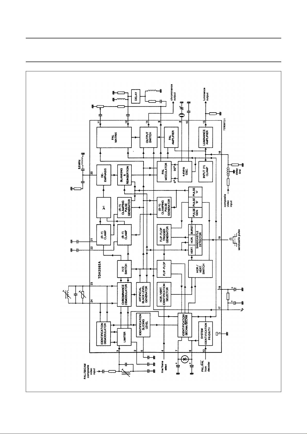
Fig.1 Block diagram.

Philips Semiconductors Product specification
SECAM-PAL transcoder TDA3592A
PINNING
1. Ground.
2. Limiter feedback.
3. Limiter input: chrominance input SECAM; identification input SECAM/
4. Identification selection input using a DC level to preset the identification mode.
At V
< 2,9 V the TDA3592A is preset for frame identification.
4
> 4,1 V the TDA3592A is preset for line identification.
At V
4
5. Storage capacitor input for floating level identification.
6. Storage capacitor input to SECAM/
7. Double time-constant input to SECAM/
SECAM identification circuit.
SECAM identification circuit.
8. 4,43 MHz oscillator.
9. Sequentially modulated output.
10. Decoupling capacitor for miller integrator feedback circuit.
11. Direct input chrominance signal.
12. Delayed input chrominance signal.
13. PAL/PAL input signal from PAL decoder.
14. Chrominance output signal.
15. Luminance output signal.
16. Luminance/
17. Positive supply voltage (V
SECAM input signal.
).
p
18. Decoupled positive supply voltage.
19. Three-level sandcastle pulse input.
20. De-emphasis circuit connection: R = 560 Ω; C = 1 nF.
21. Storage capacitor connection for (R−Y) clamp.
22. Storage capacitor connection for (B−Y) clamp.
23. Demodulator reference tuned circuit: nominal frequency = 4,33 MHz; nominal QL= 2,45.
24. As for pin 23.
SECAM.
FUNCTIONAL DESCRIPTION
Demodulation
The chrominance and identification demodulators of the TDA3592A both share the same reference tuned circuit (pins 23
and 24). The identification circuit automatically detects whether the incoming signal is SECAM or SECAM (NTSC, PAL
or black-and-white).
When the incoming signals are PAL they are diverted via pin 16 to the chrominance output at pin 14 and no signal
demodulation takes place. The delay line connected to pin 16 delays the signals to equalize the delay of the SECAM-PAL
transcoding process. When SECAM signals are received, the PAL signal path is switched off.
Incoming SECAM signals are applied to pin 3 via an external bell filter. The signals are amplified, limited and then
demodulated. Only one demodulator is necessary as the colour difference signals are available sequentially. After
demodulation the colour difference signals are separated by an H/2 switch and then applied to (R-Y) and (B-Y) clamp
circuits where the black levels are clamped to the same DC level. With all conditions at pin 4, artificial black levels are
inserted during the horizontal blanking periods. This is done because of the possibility of horizontal burst signals not
being available. The artificial levels may not be identical to the detected black level due to circuit spread but this can be
corrected by detuning the reference tuned circuit.
January 1988 4

Philips Semiconductors Product specification
SECAM-PAL transcoder TDA3592A
The two colour difference signals are combined again after clamping and then applied to the modulator via de-emphasis,
blanking and reinsertion circuits. The ratio of (R-Y) to (B-Y) at the de-emphasis output (pin 20) is 1,78.
Modulation
A burst signal is reinserted into the combined SECAM signal at the input to the PAL modulator. At this input the phase
relationship for magenta colour is +(R-Y) and−(B-Y). The modulation carriers for the (R-Y) and (B-Y) signals are 90° out
of phase; for a magenta colour the modulated (R-Y) component has the same phase position as the (R-Y) burst. The
(B-Y) burst is modulated 180° out of phase with respect to the (B-Y) component of a magenta-coloured input signal.
Identification SECAM/SECAM
Identification of the SECAM signal is performed using the fact that only SECAM signals have a line-to-line difference in
voltage level. The identification circuit compares the phase of the demodulated voltage difference waveform with the
phase of the flip-flop output. If the phase relationship is not correct, the flip-flop is reset by an extra pulse from the flip-flop
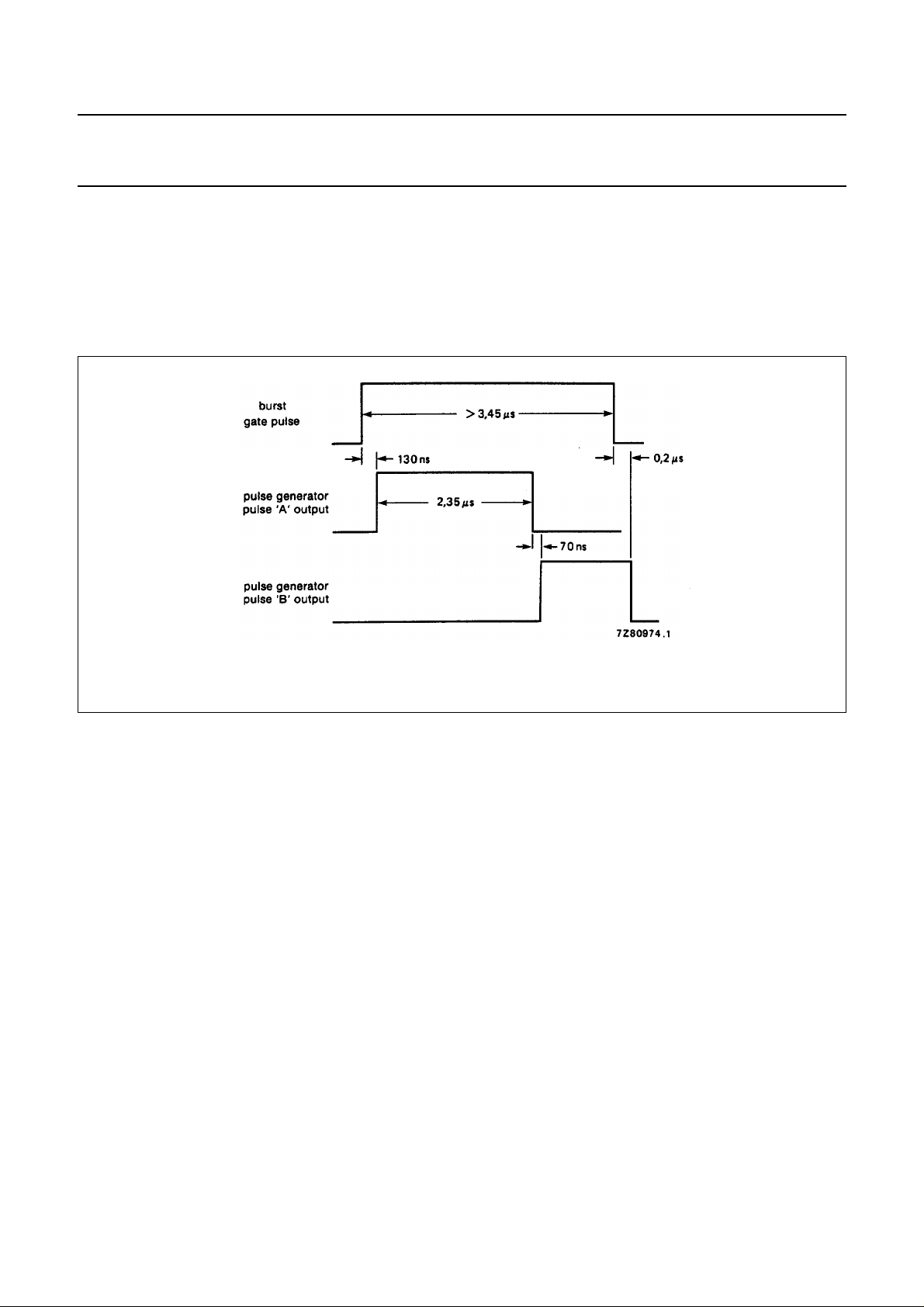
trigger generator. For horizontal identification the phase comparison is performed during the period of pulse ‘B’ (see
Fig.2). When vertical identification is selected, the comparison is performed only during the horizontal scan of the vertical
blanking. The SECAM identification circuits operate when selected by the voltage on pin 4; this may be horizontal, vertical
or combined horizontal and vertical identification, depending on the switching arrangements of pin 4.
These are as follows:
• Horizontal identification preset when V
• Vertical identification preset when V
• Horizontal/vertical combination when sandcastle pulse is present on pin 4.
4-1
< 2,9 V;
4-1
> 4,1 V;
Information obtained from the identification detector is also used for colour killing and, if required, for switching to PAL.
January 1988 5

Philips Semiconductors Product specification
SECAM-PAL transcoder TDA3592A
Sandcastle pulse detection
The sandcastle pulse detector requires a three-level sandcastle pulse to provide horizontal blanking, vertical blanking
and burst gate pulses. The detector burst gate pulse triggers a pulse generator which produces two timing pulses, pulse
‘A’ and pulse ‘B’ (see Fig.2). Pulse ‘A’ is used to time the PAL modulator burst and to sample the (R-Y) and (B-Y)
clamping pulse generators. A (R-Y) clamping pulse is generated only during a red line and a (B-Y) clamping pulse only
during a blue line. Pulse ‘B’ times the SECAM horizontal identification.
Fig.2 Burst gate timing pulse generation.
Carrier generation
The carrier signal for the PAL modulator is obtained from a 4,43 MHz oscillator. An internal Miller integrator operates in
conjunction with the decoupling capacitor at pin 10 to provide the required 90° phase shift.
PAL matrix
The signal output from the PAL modulator at pin 9 is sequentially modulated with (R-Y) burst phased in the +(R-Y)
direction, and (B-Y) burst phased in the −(B-Y) direction. This PAL signal is applied directly to pin 11 and via a 64 µs
delay to pin 12. A true PAL signal is constructed in the PAL matrix by means of an additional/substraction process (in a
correct H/2 sequence) using the delayed and undelayed inputs.
January 1988 6
 Loading...