

Philips TDA3566A Datasheet

INTEGRATED CIRCUITS
TDA3566A
PAL/NTSC decoder
Product specification
Supersedes data of March 1991
File under Integrated Circuits, IC02
Philips Semiconductors
February 1994

Philips Semiconductors Product specification
PAL/NTSC decoder TDA3566A
FEATURES
• A black-current stabilizer which
controls the black-currents of the
three electron-guns to a level low
enough to omit the black-level
adjustment
• Contrast control of inserted RGB
signals
• No black-level disturbance when
non-synchronized external RGB
signals are available on the inputs
APPLICATIONS
• Teletext/broadcast antiope
• Channel number display.
GENERAL DESCRIPTION
The TDA3566A is a decoder for the
PAL and/or NTSC colour television
standards. It combines all functions
required for the identification and
demodulation of PAL/NTSC signals.
Furthermore it contains a luminance
amplifier, an RGB-matrix and
amplifier. These amplifiers supply
output signals up to 4 V peak-to-peak
(picture information) enabling direct
drive of the discrete output stages.
The circuit also contains separate
inputs for data insertion, analog and
digital, which can be used for text
display systems.
• NTSC capability with hue control.
QUICK REFERENCE DATA
All voltages referenced to ground.
SYMBOL PARAMETER MIN. TYP. MAX. UNIT
Supply
V
P
I
P
supply voltage (pin 1) − 12 − V
supply current (pin 1) − 90 − mA
Luminance amplifier (pin 8)
V
8(p-p)
input voltage (peak-to-peak value) − 450 − mV
CON contrast control − 16.5 − dB
Chrominance amplifier (pin 4)
V
4(p-p)
input voltage (peak-to-peak value) 40 − 1100 mV
SAT saturation control − 50 − dB
RGB matrix and amplifiers
V
13, 15, 17(p-p)
output voltage at nominal luminance and contrast
− 3.8 − V
(peak-to-peak value)
Data insertion
V
12, 14, 16(p-p)
input signals (peak-to-peak value) − 1 − V
Data blanking (pin 9)
V
9
input voltage for data insertion 0.9 − − V
Sandcastle input (pin 7)
V
7
V
7
blanking input voltage − 1.5 − V
burst gating and clamping input voltage − 7 − V
ORDERING INFORMATION
EXTENDED TYPE
NUMBER
PINS PIN POSITION MATERIAL CODE
PACKAGE
TDA3566A 28 DIL plastic SOT117
February 1994 2
Philips Semiconductors Product specification
27
TDA3566A
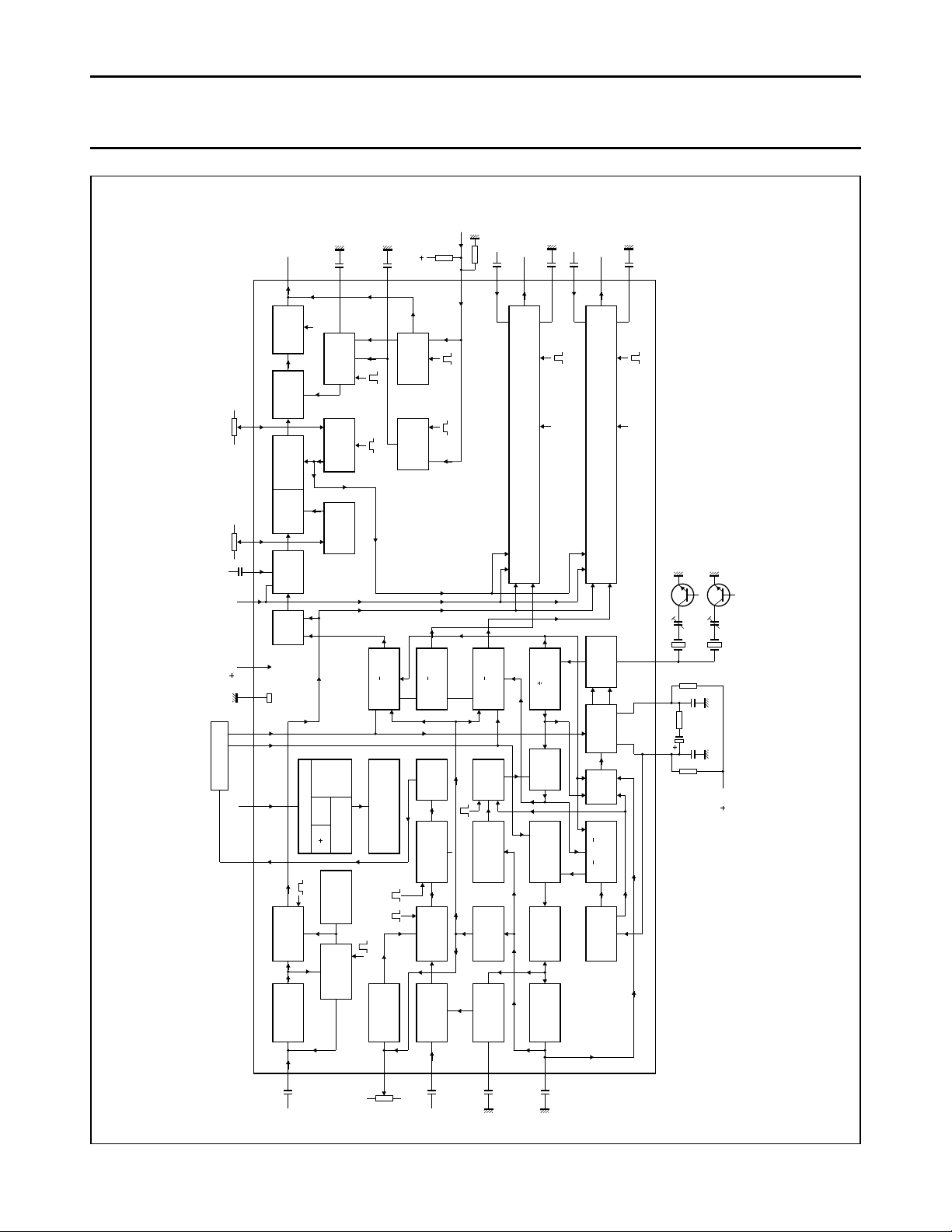
AMPLIFIER
BLACK LEVEL
INSERTION
BLACK LEVEL
CLAMPING
BLACK LEVEL
REFERENCE
(4L)
LIN/LOG
CONVERTER
CONTROLLED
CHROMINANCE
AMPLIFIER
PEAK
DETECTOR
CLAMPED
DETECTOR
GATED
SATURATION
CONTROL
KILLER
DETECTOR
AMPLIFIER
PAL/NTSC
MODE
SWITCH
GATED
CHROMINANCE
AMPLIFIER
IDENTIFICATION
H/2
DETECTOR
(R Y) (B Y)
REFERENCE
SWITCH
BUFFER
PAL
FLIP-FLOP
PAL
SWITCH
PHASE
GATED
BURST
DETECTOR
8.8 MHz
OSCILLATOR
2
90 SHIFT
o
(R Y)
DEMODULATOR
(G Y)
MATRIX
(B Y)
DEMODULATOR
SANDCASTLE DETECTOR
BURST
GATING
BLANKING
H V H
I L LOGIC &
BUFFER STAGES
2
12 V
8.8 MHz crystal (PAL)
7.16 MHz crystal (PAL/NTSC)
25 24 26
B
MATRIX
DATA
SWITCH
STAGE
CONTRAST BRIGHTNESS
LIN/LOG
CONVERTOR
BRIGHTNESS
isolation
pulse
(4L)
AMPLIFIER
BUFFER
&
BLANKING
BLACK
LEVEL
CLAMPING
clamp
pulse
(L3)
LEAKAGE
CURRENT
CLAMPING
DELAYED
SWITCH-ON
clamp
pulse
(L2)
(L0)
clamp
pulse
(L1)
blanking
(BL1)
RED
output
RED
insertion
12
13
10
clamp
pulse
(L1)
blanking
(BL1)
GREEN
output
GREEN
insertion
14
15
21
black
current
information
(M)
BLUE
output
DELAY LINE
sandcastle
pulse
blanking
(BL3)
contrast
BLUE
insertion
data
blanking
12 V
1 9 16 62223728 11
brightness
17
20
19
18
luminance
input
saturation
chrominance
input
8
5
4
3
2
Fig.1 Block diagram.
For explanation of pulse mnemonics see Fig. 7.
PAL/NTSC decoder TDA3566A
MGA819
February 1994 3
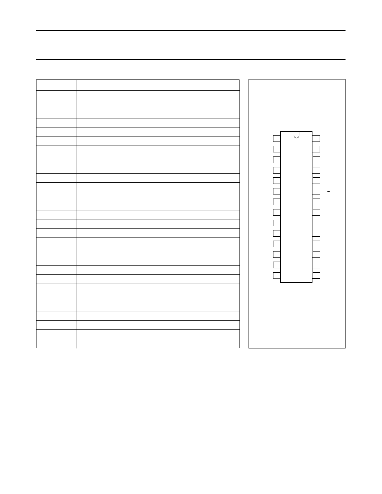
Fig.2 Pin configuration.
1
2
3
4
5
6
7
8
9
10
11
12
13
28
27
26
25
24
23
22
21
20
19
18
17
16
1514
V
P
IDDET
ACCDET
CHR
SAT
CON
SC
LUM
DBL
BCL
R
BRI
R
IN
R
OUT
G
IN
TDA3566A
CHR
OUT
GND
OSC
RCEXT
RCEXT
R Y
B Y
BCL
G
BCL
B
BCL
BLA
B
OUT
B
IN
G
OUT
MLA407
IN
Philips Semiconductors Product specification
PAL/NTSC decoder TDA3566A
PINNING
SYMBOL PIN DESCRIPTION
V
P
IDDET 2 identification detection level
ACCDET 3 Automatic Chrominance Control detection level
CHR
IN
SAT 5 saturation control input
CON 6 contrast control input
SC 7 sandcastle input
LUM 8 luminance control input
DBL 9 data blanking input
BCL
R
BRI 11 brightness input
R
IN
R
OUT
G
IN
G
OUT
B
IN
B
OUT
BLA 18 black current input
BCL 19 black clamp level; referenced to black level
BCL
B
BCL
G
OUT
B−Y 22 demodulator input (BLUE)
R−Y 23 demodulator input (RED)
RCEXT 24 gated burst detector load network
RCEXT 25 gated burst detector load network
OSC 26 oscillator frequency input
GND 27 ground
CHR
1 supply voltage
4 chrominance control input
10 black clamp level for RED output
12 RED input
13 RED output
14 GREEN input
15 GREEN output
16 BLUE input
17 BLUE output
20 black clamp level for BLUE output
21 black clamp level for GREEN output
28 chrominance signal output
February 1994 4

Philips Semiconductors Product specification
PAL/NTSC decoder TDA3566A
FUNCTIONAL DESCRIPTION
The TDA3566A is a further
development of the TDA3562A. It has
the same pinning and nearly the
same application. The differences
between the TDA3562A and the
TDA3566A are as follows:
• The NTSC-application has largely
been simplified. In the event of
NTSC the chrominance signal is
now internally coupled to the
demodulators, automatic
chrominance control (ACC) and
phase detectors. The chrominance
output signal (pin 28) is thus
suppressed. It follows that the
external switches and filters which
are required for the TDA3562A are
not required for the TDA3566A.
There is no difference between the
amplitudes of the colour output
signals in the PAL or NTSC mode.
• The clamp capacitor at pins 10, 20
and 21 in the black-level
stabilization loop can be reduced to
100 nF provided the stability of the
loop is maintained. Loop stability
depends on complete application.
The clamp capacitors receive a
pre-bias voltage to avoid coloured
background during switch-on.
• The crystal oscillator circuit has
been changed to prevent parasitic
oscillations on the third overtone of
the crystal. Consequently the
optimum tuning capacitance must
be reduced to 10 pF.
• The hue control has been improved
(linear).
Luminance amplifier
The luminance amplifier is voltage
driven and requires an input signal of
450 mV peak-to-peak (positive
video). The luminance delay line must
be connected between the IF
amplifier and the decoder.
The input signal is AC coupled to the
input (pin 8). After amplification, the
black level at the output of the
preamplifier is clamped to a fixed DC
level by the black level clamping
circuit. During three line periods after
vertical blanking, the luminance
signal is blanked out and the black
level reference voltage is inserted by
a switching circuit.
This black level reference voltage is
controlled via pin11 (brightness). At
the same time the RGB signals are
clamped. Noise and residual signals
have no influence during clamping
thus simple internal clamping circuitry
is used.
Chrominance amplifiers
The chrominance amplifier has an
asymmetrical input. The input signal
must be AC coupled (pin 4) and have
a minimum amplitude of
40 mV peak-to-peak.
The gain control stage has a control
range in excess of 30 dB, the
maximum input signal must not
exceed 1.1 V peak-to-peak,
otherwise clipping of the input signal
will occur.
From the gain control stage the
chrominance signal is fed to the
saturation control stage. Saturation is
linearly controlled via pin 5. The
control voltage range is 2 to 4 V, the
input impedance is high and the
saturation control range is in excess
of 50 dB.
The burst signal is not affected by
saturation control. The signal is then
fed to a gated amplifier which has a
12 dB higher gain during the
chrominance signal. As a result the
signal at the output (pin 28) has a
burst-to-chrominance ratio which is
6 dB lower than that of the input
signal when the saturation control is
set at −6 dB.
The chrominance output signal is fed
to the delay line and, after matrixing,
is applied to the demodulator input
pins (pins 22 and 23). These signals
are fed to the burst phase detector. In
the event of NTSC the chrominance
signal is internally coupled to the
demodulators, ACC and phase
detectors.
Oscillator and identification circuit
The burst phase detector is gated
with the narrow part of the sandcastle
pulse (pin 7). In the detector the
(R−Y) and (B−Y) signals are added to
provide the composite burst signal
again.
This composite signal is compared
with the oscillator signal
divided-by-2 (R−Y) reference signal.
The control voltage is available at
pins 24 and 25, and is also applied to
the 8.8 MHz oscillator. The 4.4 MHz
signal is obtained via the divide-by-2
circuit, which generates both the
(B−Y) and (R−Y) reference signals
and provides a 90° phase shift
between them.
The flip-flop is driven by pulses
obtained from the sandcastle
detector. For the identification of the
phase at PAL mode, the (R−Y)
reference signal coming from the PAL
switch, is compared to the vertical
signal (R−Y) of the PAL delay line.
This is carried out in the H/2 detector,
which is gated during burst.
When the phase is incorrect, the
flip-flop gets a reset from the
identification circuit. When the phase
is correct, the output voltage of the
H/2 detector is directly related to the
burst amplitude so that this voltage
can be used for the ACC.
To avoid 'blooming-up' of the picture
under weak input signal conditions
the ACC voltage is generated by peak
detection of the H/2 detector output
signal. The killer and identification
circuits receive their information from
a gated output signal of H/2 detector.
Killing is obtained via the saturation
control stage and the demodulators to
obtain good suppression.
February 1994 5

Philips Semiconductors Product specification
PAL/NTSC decoder TDA3566A
The time constant of the saturation
control (pin 5) provides a delayed
switch-on after killing. Adjustment of
the oscillator is achieved by variation
of the burst phase detector load
resistance between pins 24 and 25
(see Fig.8).
With this application the trimmer
capacitor in series with the 8.8 MHz
crystal (pin 26) can be replaced by a
fixed value capacitor to compensate
for unbalance of the phase detector.
Demodulator
The (R−Y) and (B−Y) demodulators
are driven by the colour difference
signals from the delay-line matrix
circuit and the reference signals from
the 8.8 MHz divider circuit. The (R−Y)
reference signal is fed via the
PAL-switch. The output signals are
fed to the R and B matrix circuits and
to the (G−Y) matrix to provide the
(G−Y) signal which is applied to the
G-matrix. The demodulation circuits
are killed and blanked by by-passing
the input signals.
NTSC mode
The NTSC mode is switched on when
the voltage at the burst phase
detector outputs (pins 24 and 25) is
adjusted below 9 V.
To ensure reliable application the
phase detector load resistors are
external. When the TDA3566A is
used only for PAL these two 33 kΩ
resistors must be connected to +12 V
(see Fig.8).
For PAL/NTSC application the value
of each resistor must be reduced to
20 kΩ (with a tolerance of 1%) and
connected to the slider of a
potentiometer (see Fig.9). The
switching transistor brings the voltage
at pins 24 and 25 below 9 V which
switches the circuit tot the NTSC
mode.
The position of the PAL flip-flop
ensures that the correct phase of the
(R−Y) reference signal is supplied to
the (R−Y) demodulator.
The drive to the H/2 detector is now
provided by the (B−Y) reference
signal. In the PAL mode it is driven by
the (R−Y) reference signal. Hue
control is realized by changing the
phase of the reference drive to the
burst phase detector.
This is achieved by varying the
voltage at pins 24 and 25 between
7.0 V and 8.5 V, nominal position
7.65 V. The hue control characteristic
is shown in Fig.6.
RGB matrix and amplifiers
The three matrix and amplifier circuits
are identical and only one circuit will
be described.
The luminance and the colour
difference signals are added in the
matrix circuit to obtain the colour
signal, which is then fed to the
contrast control stage.
The contrast control voltage is
supplied to pin 6 (high-input
impedance). The control range is
+5 dB to −11.5 dB nominal. The
relationship between the control
voltage and the gain is linear (see
Fig.3).
During the 3-line period after blanking
a pulse is inserted at the output of the
contrast control stage. The amplitude
of this pulse is varied by a control
voltage at pin 11. This applies a
variable offset to the normal black
level, thus providing brightness
control.
The brightness control range is 1 V to
3.6 V. While this offset level is
present, the black-current input
impedance (pin 18) is high and the
internal clamp circuit is activated. The
clamp circuit then compares the
reference voltage at pin 19 with the
voltage developed across the
external resistor network RA and
RB(pin 18) which is provided by
picture tube beam current.
The output of the comparator is
stored in capacitors connected from
pins 10, 20 and 21 to ground which
controls the black level at the output.
The reference voltage is composed
by the resistor divider network and the
leakage current of the picture tube
into this bleeder. During vertical
blanking, this voltage is stored in the
capacitor connected to pin 19, which
ensures that the leakage current of
the CRT does not influence the black
current measurement.
The RGB output signals can never
exceed a level of 10.6 V. When the
signal tends to exceed this level the
output signal is clipped. The black
level at the outputs (pins 13, 15 and
17) will be approximately 3 V. This
level depends on the spread of the
guns of the picture tube. If a beam
current stabilizer is not used it is
possible to stabilize the black levels at
the outputs, which in this application
must be connected to the black
current measuring input (pin 18) via a
resistor network.
February 1994 6

Philips Semiconductors Product specification
PAL/NTSC decoder TDA3566A
Data insertion
Each colour amplifier has a separate
input for data insertion.
A 1 V peak-to-peak input signal
provides a 3.8 V peak-to-peak output
signal.
To avoid the black-level of the
inserted signal differing from the black
level of the normal video signal, the
data is clamped to the black level of
the luminance signal. Therefore AC
coupling is required for the data
inputs.
To avoid a disturbance of the blanking
level due to the clamping circuit, the
source impedance of the driver circuit
voltage at this pin exceeds a level of
0.9 V, the RGB matrix circuits are
switched off and the data amplifiers
are switched on.
To avoid coloured edges, the data
blanking switching time is short. The
amplitude of the data output signals is
controlled by the contrast control at
pin 6. The black level is equal to the
video black level and can be varied
between 2 and 4 V (nominal
condition) by the brightness control
voltage at pin 11.
Non-synchronized data signals do not
disturb the black level of the internal
signals.
must not exceed 150 Ω. The data
insertion circuit is activated by the
data blanking input (pin 9). When the
LIMITING VALUES
In accordance with the Absolute Maximum Rating System (IEC 134).
Blanking of RGB and data signals
Both the RGB and data signals can
be blanked via the sandcastle input
(pin 7). A slicing level of 1.5 V is used
for this blanking function, so that the
wide part of the sandcastle pulse is
separated from the remainder of the
pulse. During blanking a level of +1 V
is available at the output. To prevent
parasitic oscillations on the third
overtone of the crystal the optimum
tuning capacitance should be 10 pF.
SYMBOL PARAMETER MIN. MAX. UNIT
V
P
P
tot
T
amb
T
stg
supply voltage (pin 1) − 13.2 V
total power dissipation − 1700 mW
operating ambient temperature −25 +70 °C
storage temperature −25 +150 °C
THERMAL RESISTANCE
SYMBOL PARAMETER THERMAL RESISTANCE
R
th j-a
from junction to ambient in free air 40 K/W
February 1994 7

Philips Semiconductors Product specification
PAL/NTSC decoder TDA3566A
CHARACTERISTICS
VP = 12 V; T
SYMBOL PARAMETER CONDITIONS MIN. TYP. MAX. UNIT
Supply
V
P
I
P
P
tot
Luminance input (pin 8)
V
8(p-p)
V
8
I
8
I
6
Chrominance amplifier
V
4(p-p)
Z
4
C
4
∆V change of the burst signal at the output
G amplification at nominal saturation
V
28(p-p)
d distortion of chrominance amplifier at
α
28-4
I
5
S/N signal-to-noise ratio at nominal input
∆ϕ phase shift burst with respect to
Z
28
= 25 °C; all voltages are referenced to pin 27; unless otherwise specified.
amb
supply voltage 10.8 12.0 13.2 V
supply current − 90 120 mA
total power dissipation − 1.1 1.6 W
input voltage (peak-to-peak value) note 1 − 0.45 0.63 V
input voltage level before clipping
− − 1.4 V
occurs in the input stage
input current − 0.1 1 µA
contrast control range see Fig.3 −11.5 − +5 dB
input current contrast control − − 15 µA
input signal amplitude
note 2 40 390 1100 mV
(peak-to-peak value)
input impedance − 10 − kΩ
input capacitance − − 6.5 pF
ACC control range 30 − − dB
control range
100 mV to
1 V (p-p)
− − 1 dB
note 3 34 − − dB
(pin 4 to pin 28)
chrominance to burst ratio at nominal
− 7 − dB
saturation
maximum output voltage range
RL = 2 kΩ 4 5 − V
(peak-to-peak value)
− − 5 %
2 V (p-p) output signal up to an input
signal of 1 V (p-p)
frequency response between 0 and
− − −2 dB
5 MHz
saturation control range see Fig.4 50 − − dB
input current saturation control − − 20 µA
cross-coupling between luminance and
note 4 − − −46 dB
chrominance amplifier
note 5 56 − − dB
signal
− − ±5 deg
chrominance at nominal saturation
output impedance of chrominance
− 10 − Ω
amplifier
February 1994 8
 Loading...