

Philips tda3565 DATASHEETS
INTEGRATED CIRCUITS
DATA SH EET
TDA3565
PAL decoder
Product specification
File under Integrated Circuits, IC02
April 1986

Philips Semiconductors Product specification
PAL decoder TDA3565
GENERAL DESCRIPTION
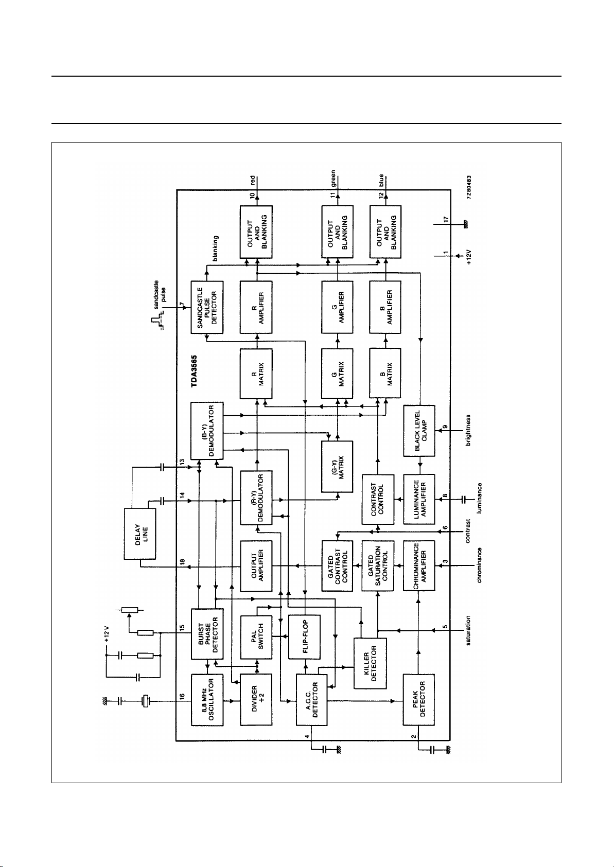
The TDA3565 PAL decoder contains all the functions required for PAL signal decoding and colour matrixing and is
contained within an 18-pin package. The oscillator, a.c.c. detector and burst phase detector each have single-pin outputs
and the coupling capacitor for the luminance input at pin 8 doubles as a storage capacitor for the black level clamping
circuit. Black level clamping of the three colour channels is performed using feedback proportional to the red channel
black level. This feedback (variable with the brightness control) controls the input level of the luminance amplifier and
therefore the clamping levels of all three colour signal outputs.
QUICK REFERENCE DATA
Supply voltage V
Supply current I
Luminance input signal (peak-to-peak value) V
Chrominance input signal (peak-to-peak value) V
p=V1-17
p=I1
8-17(p-p)
3-17(p-p)
typ. 12 V
typ. 85 mA
typ. 0,45 V
typ. 550 mV
RGB output signal amplitudes (peak-to-peak value)
at nominal luminance and contrast V
10,11,12-17(p-p)
typ. 5 V
Contrast control range −17 to +3dB
Saturation control range > 50 dB
A.C.C. control range > 30 dB
Level at which RGB blanking is activated V
Level at which burst gate/clamping pulse are separated V
7-17
7-17
typ. 1,5 V
typ. 7 V
PACKAGE OUTLINE
18-lead DIL; plastic (SOT102); SOT102-1; 1996 November 21.
April 1986 2
Philips Semiconductors Product specification
PAL decoder TDA3565
April 1986 3
Fig.1 Block diagram.

Philips Semiconductors Product specification
PAL decoder TDA3565
RATINGS
Limiting values in accordance with the Absolute Maximum System (IEC 134)
Supply voltage (pin 1) V
Total power dissipation P
Operating ambient temperature range T
Storage temperature range T
THERMAL RESISTANCE
P
tot
amb
stg
= V
1-17
max. 13,2 V
max. 1,7 W
−25 to +65 °C
−25 to +150 °C
From junction to ambient (in free air) R
th j-a
max. 50 K/W
CHARACTERISTICS
V
P=V1-17
= 12 V; T
=25°C unless otherwise specified
amb
PARAMETER SYMBOL MIN. TYP. MAX. UNIT
Supply (pin 1)
Supply voltage V
Supply current I
Total power dissipation P
1-17
1
tot
9,0 12,0 13,2 V
− 85 − mA
− 1,0 − W
Luminance amplifier
Input signal amplitude (note 2)
(peak-to-peak value) V
Input level before clipping occurs (note 1) V
Input current at V
8-17
=2V;
clamp not active I
8-17(p-p)
8-17(p-p)
8
− 0,45 − V
−− 0,7 V
− 0,15 1,0 µA
Contrast control range (Fig.2) −−17 to +3 − dB
Input current when peak white
limiter is active (V
Input resistance V
= 2,5 V) I
6-17
> 6V R
6-17
8
i
− 5,5 − mA
1,4 2,0 2,6 kΩ
Chrominance amplifier
Input signal amplitude (note 3) V
3-17(p-p)
55 550 1100 mV
Minimum burst signal amplitude
within the control range (peak-peak) 30 −−mV
Input impedance Z
Input capacitance C
3-17
3-17
− 8,0 − kΩ
− 4,0 6,0 pF
A.C.C. control range 30 −−dB
Change of burst signal at output
over whole a.c.c. control range −− 1dB
Amplification pin 3 to pin 18 at
nominal contrast/saturation (note 4) 32 −−dB
April 1986 4
 Loading...