Philips TDA2653A Datasheet

INTEGRATED CIRCUITS
DATA SH EET
TDA2653A
Vertical deflection circuit
Product specification
File under Integrated Circuits, IC02
January 1991

Philips Semiconductors Product specification
Vertical deflection circuit TDA2653A
DESCRIPTION
The TDA2653A is a monolithic integrated circuit for vertical deflection in large screen colour television receivers.
The circuit incorporates the following functions:
• Oscillator; switch capability for 50 Hz/60 Hz operation
• Synchronization circuit
• Blanking pulse generator with guard circuit
• Sawtooth generator with buffer stage
• Preamplifier with fed-out inputs
• Output stage with thermal and short-circuit protection
• Flyback generator
• Voltage stabilizers
QUICK REFERENCE DATA
Supply voltage (pin 9) V
Supply current (pin 5 + pin 9)
Output current (peak-to-peak value)
(1)
(1)
Maximum output current (peak-to-peak value) I
9-8=VS
I5+ I9=I
I
6(p-p)
6(p-p)
S
typ. 26 V
typ. 325 mA
typ. 1,7 A
max. 2,6 A
Picture frequency f 50 Hz/60 Hz
Sync input pulse (peak-to-peak value) V
Thermal resistance from junction to mounting base R
2-8(p-p)
th j-mb
≥ 1 V
≤ 5 K/W
Note
1. for 45 AX systems
PACKAGE OUTLINE
13-lead SIL; plastic power (SOT141RGA); SOT141-6; 1996 November 19.
January 1991 2

Philips Semiconductors Product specification
Vertical deflection circuit TDA2653A
(1) Condition for pin 12: LOW voltage level = 50 Hz; HIGH voltage level = 60 Hz.
Fig.1 Block diagram.
January 1991 3

Philips Semiconductors Product specification
Vertical deflection circuit TDA2653A
RATINGS
Limiting values in accordance with the Absolute Maximum System (IEC 134)
Supply voltage (pin 9) V
Supply voltage output stage (pin 5) V
Voltages
Pin 3 V
Pin 13 V
Pins 4 and 10 V
Pin 6 v
Pins 7 and 11 V
Currents
Pin 1 I
Pin 2 ±I
Pin 3 I
Pin 7 I
Pin 11 I
Pin 12 I
Pins 5, 6 and 8: internally limited by the short-circuit protection circuit.
Total power dissipation: internally limited by the thermal protection circuit.
Storage temperature range T
Operating ambient temperature range T
9−8
5-8
3−11
13-8
4; 10-8
6-8
−V
7; 11−8
1
−I
1
2
3
−I
3
7
−I
7
11
−I
11
12
−I
12
stg
amb
6−8
= V
S
max. 40 V
max. 60 V
max. 7 V
max. 7 V
max. 24 V
max. 60 V
max. 0 V
max. 40 V
max. 0 mA
max. 1 mA
max. 10 mA
max. 0 mA
max. 5 mA
max. 1,3 A
max. 1,5 A
max. 50 mA
max. 1 mA
max. 3 mA
max. 0 mA
−25 to + 150 °C
0 °C to limiting value
January 1991 4
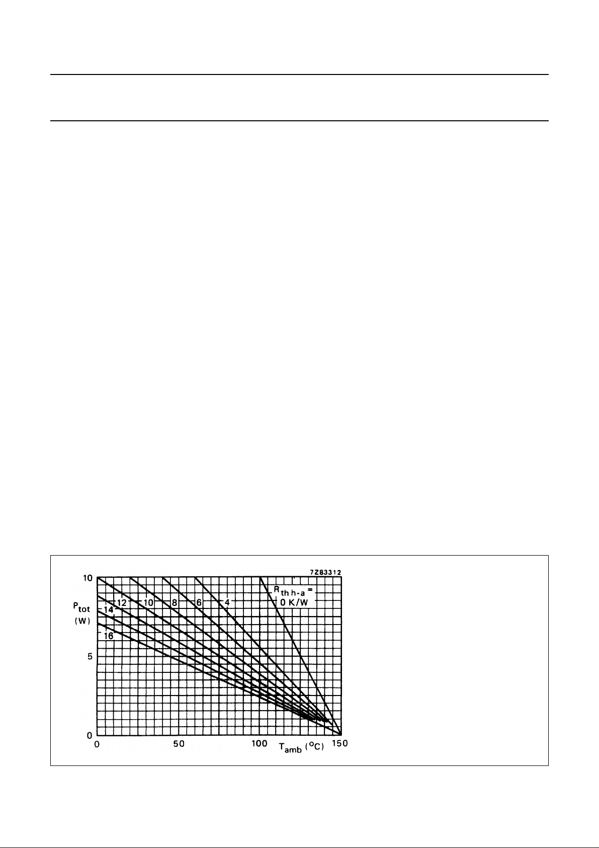
Fig.2 Total power dissipation.
R
includes R
th h-a
th mb-h
which is expected when heatsink compound is used.
R
th j−mb
≤ 5 K/W.
 Loading...