

Philips tda2052 DATASHEETS
60W Hi-Fi AUDIO POWER AMPLIFIER
SUPPLYVOLTAGERANGEUP TO±25V
SPLIT SUPPLY OPERATION
HIGHOUTPUT POWER
(UP TO 60W MUSICPOWER)
LOW DISTORTION
MUTE/STAND-BY FUNCTION
NO SWITCH ON/OFF NOISE
AC SHORT CIRCUIT PROTECTION
THERMALSHUTDOWN
ESDPROTECTION
DESCRIPTION
The TDA2052 is a monolithic integrated circuit in
Heptawatt package, intended for use as audio
class AB amplifier in TV or Hi-Fi field application.
Thanks to the wide voltage range and to the high
out current capability it’s able to supply the high-
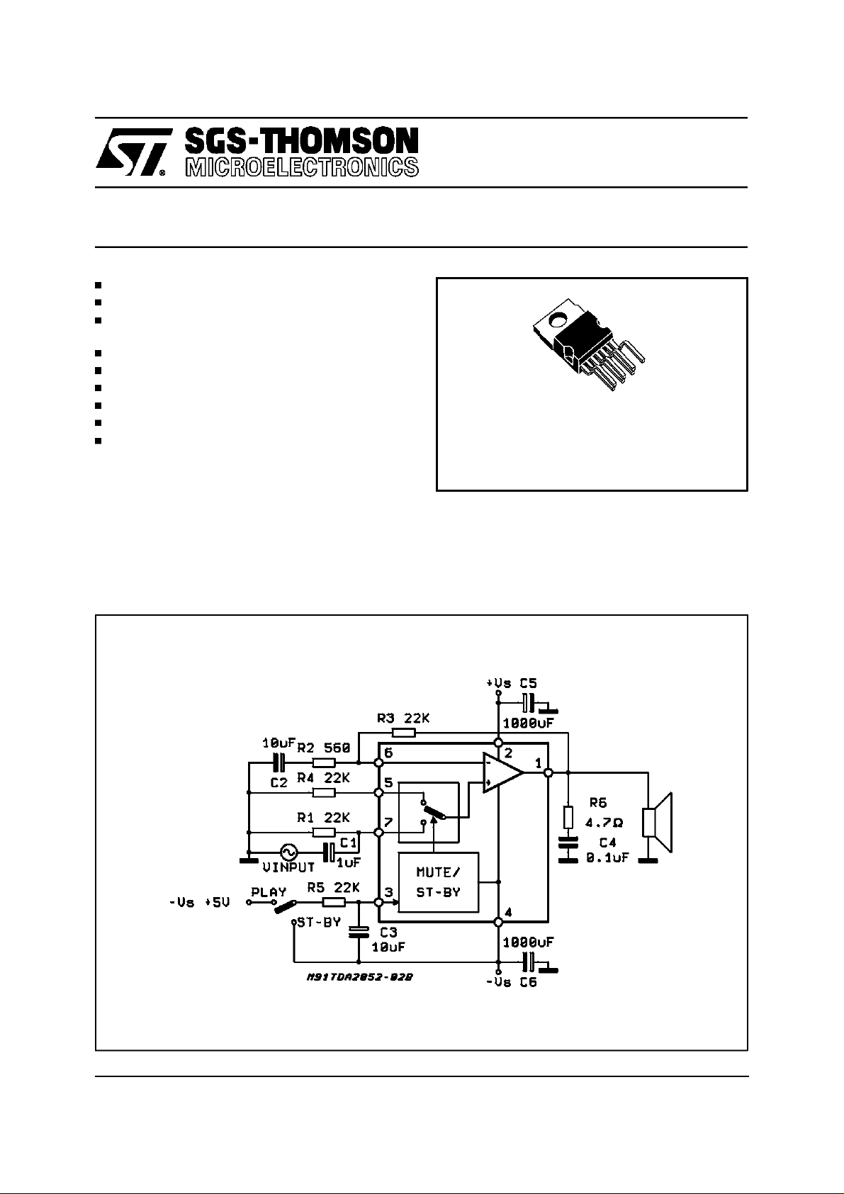
TEST ANDAPPLICATION CIRCUIT
TDA2052
WITH MUTE / STAND-BY
Heptawatt
ORDERING NUMBER: TDA2052
est power into both 4Ωand 8Ωloads even in
presenceof poorsupply regulation.
The built in Muting/Stand-by function simplifies
the remote operations avoiding also switchingonoff noises.
February 1997
This is advanced information on a new product now in developmentor undergoing evaluation. Detailsare subject to changewithoutnotice.
1/13

TDA2052
ABSOLUTE MAXIMUM RATINGS
Symbol Parameter Value Unit
V
I
O
P
tot
T
op
T
stg,Tj
PIN CONNECTION (Topview)
DC Supply Voltage ±25 V
S
Output PeakCurrent (internally limited) 6 A
Power DissipationT
=70°C30W
case
Operating Temperature Range 0 to +70 °C
Storage and Junction Temperature -40 to +150
7 NON INVERTING INPUT(PLAY)
6
5
4
3
2
1
INVERTING INPUT
NON INVERTING INPUT(MUTE)
-V
S
STAND-BY/MUTE
+V
S
OUTPUT
C
°
tab connected to pin 4
BLOCK DIAGRAM
D95AU326
2/13
TDA2052
THERMAL DATA
Symbol Description Value Unit
R
th j-case
Thermal ResistanceJunction-case Max 2.5
C/W
°
ELECTRICAL CHARACTERISTICS (Refer to the test circuit, GV= 32dB; VS+ 18V; f = 1KHz; T
25°C, unlessotherwise specified.)
Symbol Parameter Test Condition Min. Typ. Max. Unit
V
S
I
q
I
b
V
OS
I
OS
P
O
P
O
Supply Range +6 +25 V
Total Quiescent Current VS= +22V 20 40 70 mA
Input Bias Current +0.5 µA
Input Offset Voltage +15 mV
Input Offset Current +200 nA
Music Output Power
IEC268-3 Rules (*)
VS= + 22.5, RL=4Ω,
d = 10%, t = 1s 50 60 W
Output Power(continuous RMS) d = 10%
RL = 4Ω
R
=8
Ω
L
V
= +22V, RL=8Ω
S
35
30
40
22
33
d=1%
d Total Harmonic Distortion R
R
=4Ω
L
R
=8
Ω
L
V
= +22V, RL=8Ω
S
=4Ω
L
P
= 0.1 to 20W;
O
f = 100Hz to 15KHz
+ 22V, RL=8Ω
V
S
P
= 0.1 to 20W;
O
f = 100Hz to 15KHz
32
17
28
0.1
0.1
0.7
0.5
SR Slew Rate 3 5 V/µs
G
V
e
N
R
SVR Supply Voltage Rejection f = 100Hz, V
T
S
Open Loop Voltage Gain 80 dB
Total Input Noise A Curve
f = 20Hz to 20KHz
Input Resistance 500 KΩ
i
ripple =1VRMS 40 50 dB
2
310
Thermal Shutdown 145 °C
MUTE/STAND-BY FUNCTION (Ref.–VS)
=
amb
W
W
W
W
W
W
%
%
V
µ
µV
VT
ST-BY
VT
PLAY
I
q ST-BY
ATT
ST-BY
I
pin3
Note (*):
MUSIC POWER CONCEPT
MUSIC POWER is ( according tothe IEC clauses n.268-3 of Jan 83) the maximal power which theamplifier iscapable of producing across the
rated load resistance (regardlessof nonlinearity) 1 sec after the application of a sinusoidal input signalof frequency 1KHz.
According to this definition our method of measurementcomprises the followingsteps:
1) Set the voltage supply at the maximumoperating value -10%
2) Apply a input signalin the form of a 1KHztone burst of 1 sec duration; the repetition period of the signal pulses is > 60 sec
3) The output voltage is measured 1 sec from thestart of the pulse
4) Increase the input voltage until the outputsignal show a THD = 10%
5) The music power is thenV
The target of this method isto avoid excessive dissipationin theamplifier.
Stand-by - Threshold 1 1.8 V
Play Threshold 2.7 4 V
Quiescent Current @ Stand-by V
= 0.5V 1 3 mA
pin 3
Stand-by Attenuation 70 90 dB
Pin 3 Current @ Stand-by –1 +10 µA
2
/R1,where V
out
isthe output voltage measured in thecondition of point 4) and R1 is the rated load impedance
out
3/13

TDA2052
APPLICATIONS SUGGESTIONS (See Test and ApplicationCircuit)
The recommendedvalues of the external components are those shown on the application circuit. Different valuescan be used;the followingtable can help the designer.
Comp. Value Purpose Larger Than Smaller Than
R1 22K
R2 560Ω Closed LoopGain set to
R3 22K
R4 22K
R5 22K
R6 4.7
C1 1µF Input DC Decoupling Higher Low-frequency
C2 10µF Feedback DC Decoupling Higher Low-frequency
C3 10µF Stand-by TimeConstant
C4 0.100µF Frequency Stability Danger of Oscillations
C5, C6 1000µF Supply Voltage Bypass
(*) R1 =R3 = R4for POP optimization
(**) Closed Loop Gain hasto be ≥ 30dB
(*) Input Impedance Increase ofInput
Ω
Ω
(*) Increase ofGain Decrease of Gain
Ω
(*) Input Impedance @ Mute
Ω
Ω
32dB (**)
Stand-by TimeConstant
Frequency Stability Danger of oscillations Danger of oscillations
Impedance
Decrease of Gain Increase ofGain
Decrease of Input
Impedance
cut-off
cut-off
TYPICALCHARACTERISTICS
Figure 1: OutputPower vs. Supply Voltage
4/13
Figure2: Distortionvs. OutputPower
 Loading...