

Philips tda2005 DATASHEETS
®
20W BRIDGE AMPLIF IER FOR CAR RADIO
High output power : PO = 10 + 10 W@RL = 2Ω, d =
10% ; P
High reliability of the c hip and package with additional complete safety during operation thanks to
protection against :
.
.
.
.
.
Flexibility in use : bridge or stereo booster amplifiers with or without boostrap and with programmable gain and bandwidth.
Space and cost saving : v ery low number of external components, very simple mounting system with
no electrical isolation between the package and the
heatsink (one screw only).
In addition, the circuit offers
tion
= 20W@RL = 4Ω , d = 1 %.
O
OUTPUT DC AND AC SHORT CIRCUIT TO
GROUND
OV ERR ATING CHIP TEMPERATURE
LOAD DUMP VOLTAGE SURGE
FORTUITOUS OPEN GROUND
VERY INDUCTIV E LO ADS
loudspeaker protec-
during short circuit for one wire to ground.
TDA2005
MULTIWATT11
ORDERING NUMBERS : TDA2005M (Bridge Appl.)
DESCRIPTION
The TDA2005 is class B dual audio po wer amplifier
in MULTIWATT package specifically designed f or
car radio application :
are easily designed using this device that provides
a high current capability (up to 3.5 A) and that can
drive very low impedance loads (down to 1.6Ω in
TDA2005S (Stereo Appl.)
power booster amplifiers
ABSOLUTE MAXIMUM RATINGS
Symbol Parameter Value Unit
V
s
V
s
V
s
I
(*) Output Peak Current (non repetitive t = 0.1 ms) 4.5 A
o
I
(*)
o
P
tot
T
, TjStorage and Junction Temperature – 40 to 150
stg
(*) The max. output current is internally limited.
Operating Supply Voltage 18 V
DC Supply Voltage 28 V
Peak Supply Voltage (for 50 ms) 40 V
Output Peak Current (repetitive f ≥ 10 Hz)
Power Dissipation at T
case
= 60 °C
3.5 A
30 W
PIN CONNECTION
11
10
9
8
7
6
5
4
3
2
1
TAB CONNECTED TO PIN 6
D95AU318
BOOTSTRAP(1)
OUTPUT(1)
+V
S
OUTPUT(2)
BOOTSTRAP(2)
GND
INPUT+(2)
INPUT-(2)
SVRR
INPUT-(1)
INPUT+(1)
°C
September 2003
1/18
TDA2005
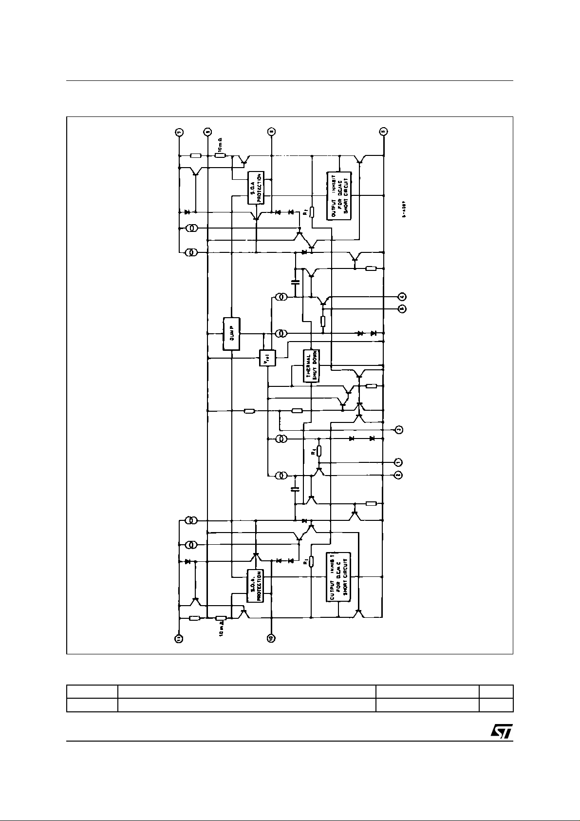
SCHEMATIC DIAGRAM
THERMAL DATA
Symbol Parameter Value Unit
2/18
R
th j-case
Thermal Resistance Junction-case Max. 3
°C/W
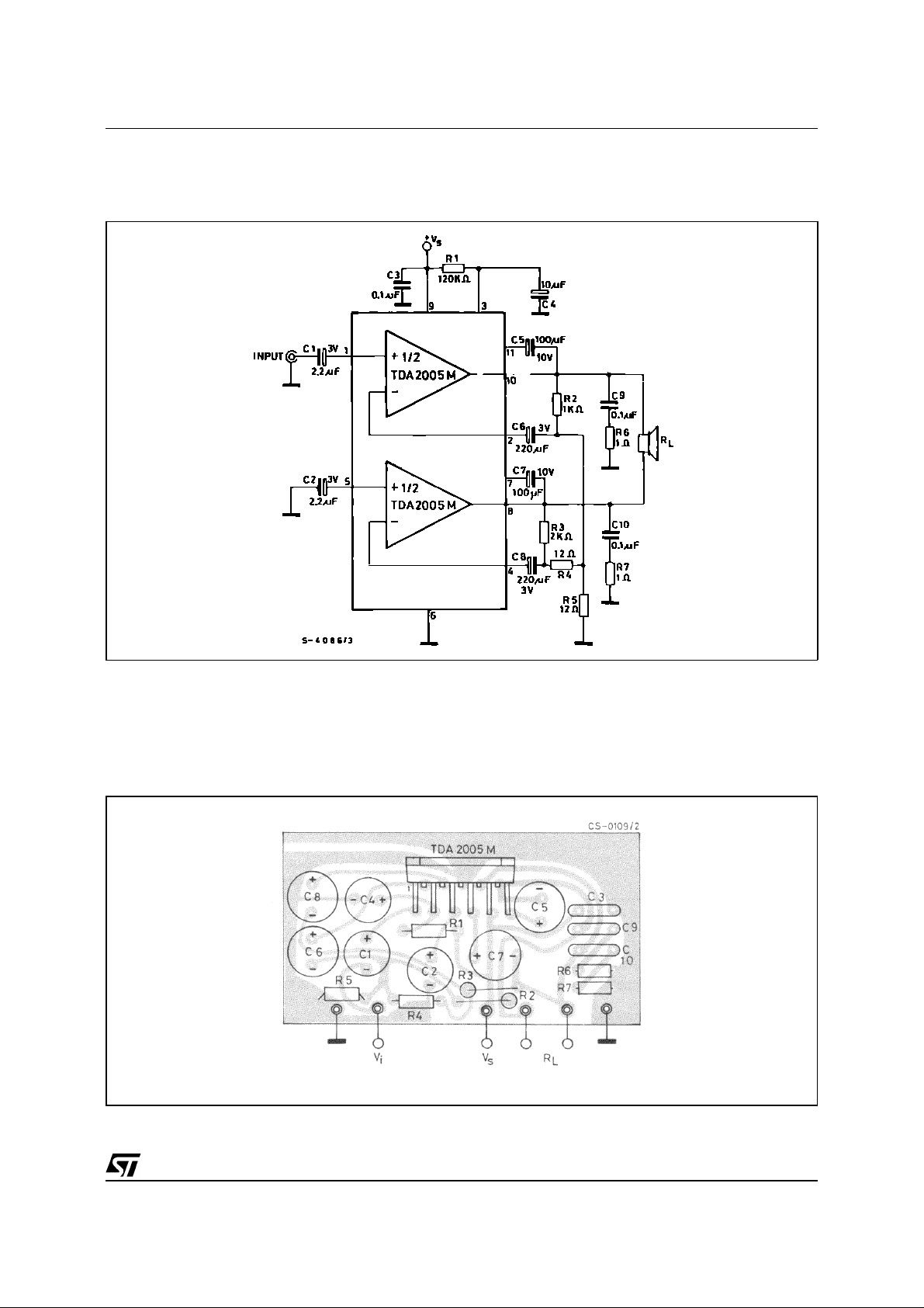
BRIDGE AMPLIFIER APPLICATION (TDA2005M)
Figure 1 : Test and Application Circuit (Bridge amplifier)
TDA2005
Figure 2 : P.C. Board and Components Layout of Figure 1 (1:1 scale)
3/18

TDA2005
ELECTRICAL CHARACTERISTICS
R
th (heatsink
) = 4oC/W, unless otherwise specified)
(refer to the
Bridge
application circuit, T
= 25oC, GV = 50dB,
amb
Symbol Parameter Test Conditions Min. Typ. Max. Unit
V
V
P
Supply Voltage 8 18 V
s
Output Offset Voltage (1)
os
(between pin 8 and pin 10)
Total Quiescent Drain Current
I
d
Output Power d = 10% f = 1 Hz
o
Vs = 14.4V
Vs = 13.2V
= 14.4V RL = 4Ω
V
s
V
= 13.2V RL = 3.2Ω
s
V
= 14.4V RL = 4Ω
s
V
= 13.2V RL = 3.2 Ω
s
R
= 3.2Ω
L
18
20
17
150
150mVmV
7570150
160mAmA
20
22
19
d Distortion f = 1kHz
V
= 14.4V RL = 4Ω
V
Input Sensitivity f = 1kHz
i
R
G
e
Input Resistance f = 1kHz 70
i
f
Low Frequency Roll Off (– 3dB)
L
f
High Frequency Roll Off (– 3dB)
H
Closed Loop Voltage Gain f = 1kHz 50 dB
v
Total Input Noise Voltage
N
SVR Supply Voltage Rejection
h Efficiency V
Thermal Shut-down Junction
T
j
Temperature
V
OSH
Output Voltage with one Side of
the Speaker shorted to ground
s
P
= 50mW to 15W
o
V
= 13.2V RL = 3.2Ω
s
Po = 50mW to 13W
P
= 2W RL = 4Ω
o
P
= 2W RL = 3.2Ω
o
R
= 3.2Ω
L
= 3.2Ω
R
L
= 10kΩ (2)
R
g
= 10kΩ, C4 = 10µF
R
g
f
= 100Hz, V
ripple
= 14.4V, f = 1 kHz
s
P
= 20W RL = 4Ω
o
P
= 22W RL = 3.2Ω
o
V
= 13.2V, f = 1 kHz
s
P
= 19W RL = 3.2Ω
o
= 14.4V, RL = 4Ω
V
s
f = 1kHz, P
V
= 14.4V RL = 4Ω
s
V
= 13.2V RL = 3.2Ω
s
tot
ripple
= 13W
= 0.5V
20 kHz
45 55 dB
60
60
58
145
1
1
9
8
40 Hz
310
2V
W
%
%
mV
mV
kΩ
µV
%
%
%
°C
Notes : 1. For TDA2005M only
2. Bandwith Filter : 22Hz to 22kHz.
4/18
TDA2005
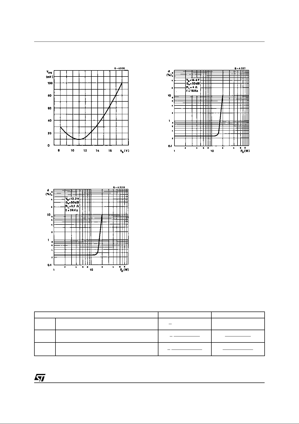
Figure 3 : Output Offset Voltage versus
Supply Voltage
Figure 5 : Distortion versus Output Power
(bridge amplifier)
Figure 4 : Distortion versus Output Power
(bridge amplifier)
BRIDGE AMPLIFIER DESIGN
The following consideraions can be useful when designing a bridge amplifier.
Parameter Single Ended Bridge
1
V
o max
I
o max
P
o max
Where : VCE
V
S
R
L
Peak Output Voltage (before clipping)
Peak Output Current (before clippling)
RMS Output Power (before clipping)
= output transistors saturation voltage
sat
= allowable supply voltage
= load impedance
(Vs – 2 V
2
V
1
S
2
(V
1
S
4
− 2 V
R
2 V
−
2 R
CE sat
CE
L
CE sat
L
sat
)
2
)
– 2 V
V
s
VS − 2 V
−
(
VS
R
2 V
2 R
CE sat
CE sat
L
CE sat
L
2
)
5/18
TDA2005
Voltage and current swings are twice for a bridge
amplifier in comparison with single ended amplifier.
In order words, with the same R
the bridge con-
L
figuration can deliver an output power that is four
times the output power of a single ended amplifier,
while, with the same max output current the bridge
configuration can deliver an output power that is
twice the output power of a single ended amplifier.
Core must be taken when selecting V
and RL in
S
order to avoid an output peak current above the
absolute maximum rating.
From the expression f or I
= 14.4V and V
= 2V, the minimum load that
CE sat
, assuming V
O max
S
can be driven by TDA2005 in bridge configuration
is :
−
R
L min
=
V
S
− 2 V
I
O
max
CEsat
=
14.4
3.5
4
= 2.97
Ω
The voltage gain of the bridge configuration is given
by (see Figure 34) :
V
0
=
G
= 1 +
V
V
1
R
R2 + R
R
2
1
⋅ R
R
3
+
R
4
4
4
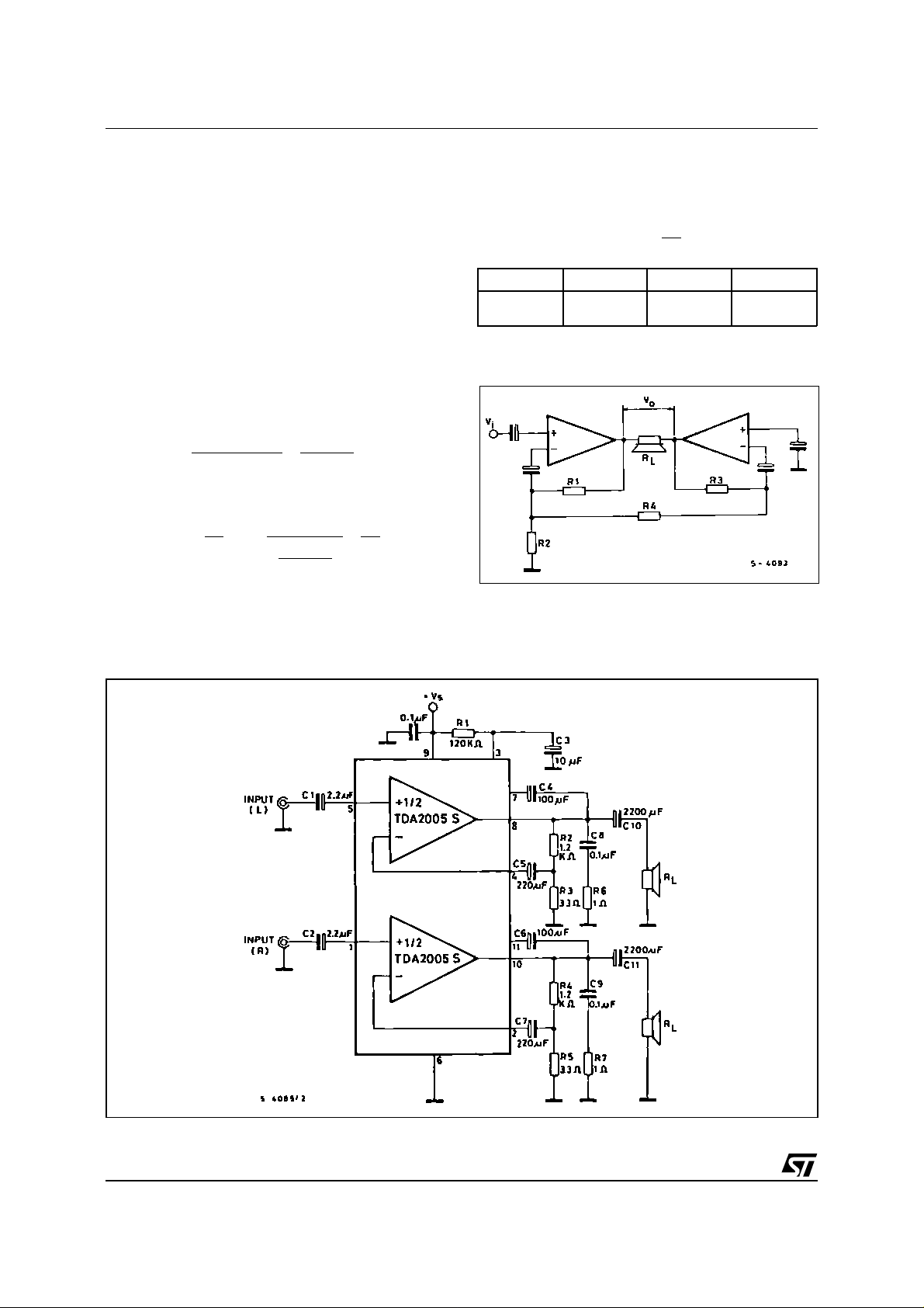
STEREO AMPLIFIER APPLIC ATION (TDA2005S )
For sufficiently high gains (40 to 50dB) it is possible
to put R
= R4 and R3 = 2 R1, simplifing the formula
2
in :
R
= 4
1
R
2
39
12
2000
2000
Gv (dB)
40
50
G
V
(Ω)R2 = R4 (Ω)R3 (Ω)
R
1
1000
1000
Figure 6 : Bridge Configuration
Figure 7 : Typical Application Circuit
6/18
 Loading...