


INTEGRATED CIRCUITS
DATA SH EET
TDA1599
IF amplifier/demodulator for FM
radio receivers
Product specification
File under Integrated Circuits, IC01
May 1994

Philips Semiconductors Product specification
IF amplifier/demodulator for FM radio
receivers
FEATURES
• Balanced limiting amplifier
• Balanced coincidence demodulator
• Two open-collector stop pulse outputs for
microcomputer tuning control
• Simulated behaviour of a ratio detector (internal field
strength and detuning dependent voltage for dynamic
AF signal muting)
• Mono/stereo blend field strength indication control
voltage
• AFC output
• 3-state mode switch for FM-MUTE-ON, FM-MUTE-OFF
and FM-OFF
• Internal compensation of AF signal total harmonic
distortion (THD)
• Built-in hum and ripple rejection circuits.
QUICK REFERENCE DATA
TDA1599
GENERAL DESCRIPTION
The TDA1599 provides IF amplification, symmetrical
quadrature demodulation and level detection for quality
home and car FM radio receivers and is suitable for mono
and stereo reception. It may also be applied to common
front ends, stereo decoders and AM receiver circuits.
SYMBOL PARAMETER MIN. TYP. MAX. UNIT
V
P
I
P
V
i
V
o
S/N signal-to-noise ratio (f
THD total harmonic distortion (f
positive supply voltage (pin 1) 7.5 8.5 12 V
supply current (I2= I7= 0) − 20 26 mA
IF input sensitivity for limiting on pin 20 (RMS value) 14 22 35 µV
AF output signal on pin 4 (RMS value) 180 200 220 mV
= 400 Hz; ∆f = ±75 kHz) − 82 − dB
m
= 1 kHz; ∆f = ±75 kHz) − 0.1 0.3 %
m
with K2 adjustment and FM-MUTE-OFF − 0.07 0.25 %
T
amb
operating ambient temperature −40 − +85 °C
All pin numbers mentioned in this data sheet refer to the SO-version (TDA1599T) unless otherwise specified.
ORDERING INFORMATION
EXTENDED
TYPE NUMBER
PINS PIN POSITION MATERIAL CODE
PACKAGE
TDA1599 18 DIL plastic SOT102
TDA1599T 20 mini-pack plastic SOT163A
Notes
1. SOT102-1; 1996 August 29.
2. SOT163-1; 1996 August 29.
(1)
(2)
May 1994 2
Philips Semiconductors Product specification
IF amplifier/demodulator for FM radio
receivers
TDA1599
May 1994 3
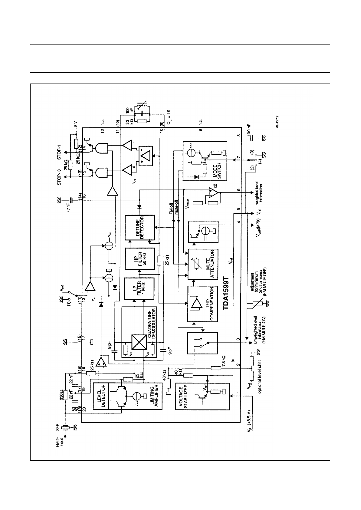
Fig.1 Block diagram and application circuit (TDA1599 pinning in parenthesis).
(1) to connect pin 13 (11) to ground is only allowed to measure the current on pin 16 (14)
(2) FM-MUTE-OFF
(3) FM-OFF
(4) FM-MUTE-ON
Philips Semiconductors Product specification
IF amplifier/demodulator for FM radio
receivers
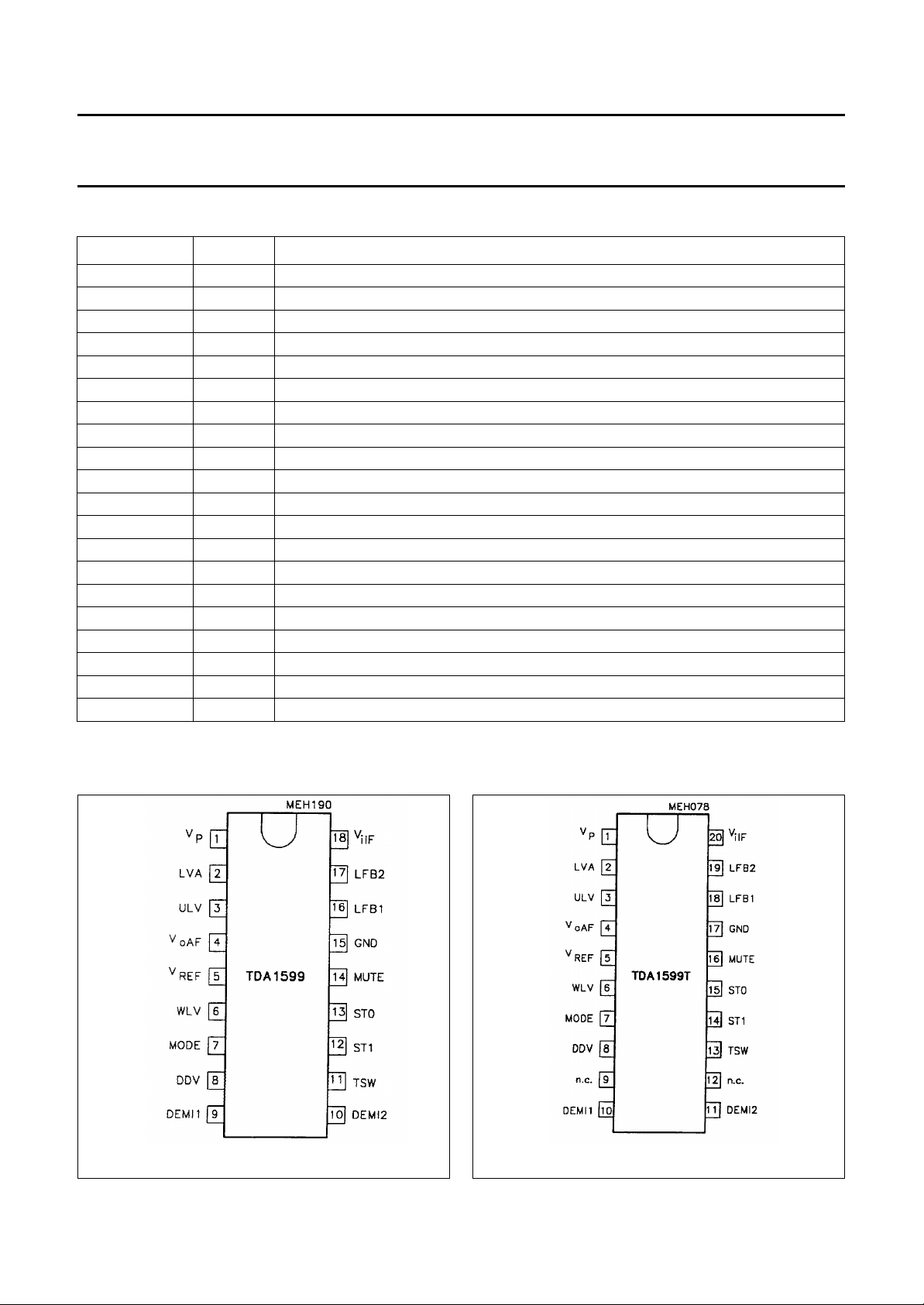
PINNING; note 1
SYMBOL PIN DESCRIPTION
V
P
LVA 2 (2) level adjustment for stop condition
ULV 3 (3) unweighted level output / K2 adjustment
V
oAF
V
REF
WLV 6 (6) weighted level output
MODE 7 (7) mode switch input
DDV 8 (8) detune detector voltage
n.c. 9 (−) not connected
DEMI1 10 (9) demodulator input 1
DEMI2 11 (10) demodulator input 2
n.c. 12 (−) not connected
TSW 13 (11) tau switch input
ST1 14 (12) STOP-1, stop pulse output 1
ST0 15 (13) STOP-0, stop pulse output 0
MUTE 16 (14) muting voltage
GND 17 (15) ground (0 V)
LFB1 18 (16) IF limiter feedback 1
LFB2 19 (17) IF limiter feedback 2
V
iIF
1 (1) supply voltage (+8.5 V)
4 (4) audio frequency output (MPX signal)
5 (5) reference voltage output
20 (18) IF signal input
TDA1599
Note
1. SO-version TDA1599T; pinning for DIL-version in parenthesis.
Fig.2 Pin configuration for DIL-version. Fig.3 Pin configuration for SO-version.
May 1994 4

Philips Semiconductors Product specification
IF amplifier/demodulator for FM radio
receivers
FUNCTIONAL DESCRIPTION
The limiter amplifier has five stages of IF amplification
using balanced differential limiter amplifiers with emitter
follower coupling.
Decoupling of the stages from the supply voltage line and
an internal high-ohmic DC feedback loop give a very stable
IF performance. The amplifier gain is virtually independent
of changes in temperature.
The FM demodulator is fully balanced and compromises
two cross-coupled differential amplifiers. The quadrature
detection of the FM signal is performed by direct feeding of
one differential amplifier from the limiter amplifier output,
and the other via an external 90 degrees phase shifting
network. The demodulator has a good stability and a small
zero-cross-over shift. The bandwidth on the demodulator
output is restricted by an internal low-pass filter to
approximately 1 MHz.
Non-linearities, which are introduced by demodulation, are
compensated by the THD compensation circuit. For this
reason, the demodulator resonance circuit (between pins
10 and 11) must have a loaded Q-factor of 19.
TDA1599
Consequently, there is no need for the demodulator tuned
circuit to be adjusted for minimum distortion. Adjustment
criterion is a symmetrical stop pulse. The control voltage
for the mute attenuator (pin 16) is derived from the values
of the level detector and the detuning detector output
signals. The mute attenuator has a fast attack and a slow
decay determined by the capacitor on pin 16. The AF
signal is fed via the mute attenuator to the output (pin 4). A
weighted control voltage (pin 6) is obtained from the mute
attenuator control voltage via a buffer amplifier that
introduces an additional voltage shift and gain.
The level detector generates a voltage output signal
proportional to the amplitude of the input signal. The
unweighted level detector output signal is available in
FM-MUTE-ON condition (mode switch).
The open-collector tuning stop output voltages STOP-0
and STOP-1 (pins 15 and 14) are derived from the
detuning and the input signal level. The pins 14 and 15
may be tied together, if only one tuning-stop output is
required.
May 1994 5

Philips Semiconductors Product specification
IF amplifier/demodulator for FM radio
TDA1599
receivers
LIMITING VALUES (TDA1599T PINNING)
In accordance with the Absolute Maximum Rating System (IEC 134).
SYMBOL PARAMETER MIN. MAX. UNIT
V
P
V
n1
V
n2
V
13
I
14, 15
P
tot
T
stg
T
amb
V
ESD
supply voltage (pin 1) −0.3 +13 V
voltage at pins 2, 4, 5, 6, 10, 11 and 16 −0.3 +10 V
voltage at pins 7, 3, 8, 14, 15, 18, 19 and 20 −0.3 V
P
voltage on pin 13 − 6V
current at pins 14 and 15 − 2mA
total power dissipation − 360 mW
storage temperature −55 +150 °C
operating ambient temperature −40 +85 °C
electrostatic handling; note 1
all pins except 5 and 7 −±2000 V
pin 5 − +800 V
−2000 V
pin 7 − +1000 V
−2000 V
V
Note to the limiting values
1. Equivalent to discharging a 100 pF capacitor through a 1.5 kΩ series resistor.
THERMAL RESISTANCE
SYMBOL PARAMETER THERMAL RESISTANCE
R
th j-a
from junction to ambient in free air
SOT102 80 K/W
SOT163A 90 K/W
May 1994 6

Philips Semiconductors Product specification
IF amplifier/demodulator for FM radio
TDA1599
receivers
CHARACTERISTICS (TDA1599T PINNING)
= 8.5 V; T
V
P
at pin 20; de-emphasis of 50 µs; tuned circuit at pins 10 and 11 aligned for symmetrical stop pulses; measurements
taken in Fig.4 unless otherwise specified.
SYMBOL PARAMETER CONDITIONS MIN. TYP. MAX. UNIT
V
P
I
P
Mode switch input
I
7
V
7
IF amplifier and demodulator
Z
i
C
i
= +25 °C; FM-MUTE-ON (I7= 0); fIF= 10.7 MHz; deviation ±22.5 kHz with fm= 400 Hz; Vi= 10 mV RMS
amb
positive supply voltage (pin 1) 7.5 8.5 12 V
supply current I2= I7= 0 − 20 26 mA
input current for FM-MUTE-ON − 0 − mA
input voltage for FM-MUTE-ON 2.4 2.8 3.2 V
input voltage for FM-MUTE-OFF 0.9V
−− V
REF
input voltage for FM-OFF AF attenuation > 60 dB −−1.4 V
demodulator input impedance
25 40 55 kΩ
between pins 10 and 11
demodulator input capacitance
− 6 − pF
between pins 10 and 11
AF output (pin 4)
R
o
V
4
RR
1000
output resistance − 400 −Ω
DC output level V
power supply ripple rejection on pin 4 f = 1000 Hz;
≤ 5 µV RMS on pin 20 2.75 3.1 3.45 V
iIF
33 36 − dB
V
=50mVRMS
ripple
Tuning stop detector
∆f detuning frequency for STOP-0 on pin 15; Fig.11
≥ 3.5 V −−+14.0 kHz
for V
15
≤ 0.3 V +22.0 −− kHz
for V
15
∆f detuning frequency for STOP-1 on pin 14; Fig.10
≥ 3.5 V −−−14.0 kHz
for V
14
≤ 0.3 V −22.0 −− kHz
for V
14
V
V
20
14, 15
dependence on input voltage for
STOP-0 and STOP-1 (RMS value)
output voltage I
Fig.9;
≥ 3.5 V 250 −− µV
V
14, 15
≤ 0.3 V −−50 µV
V
14, 15
= 1 mA −−0.3 V
14, 15
Reference voltage source (pin 5)
V
R
REF
5
reference output voltage I5= −1 mA 3.3 3.7 4.1 V
output resistance I5= −1 mA − 40 80 Ω
TC temperature coefficient − 3.3 − mV/VK
May 1994 7
 Loading...