

Page 1

INTEGRATED CIRCUITS
DATA SH EET
TDA1563Q
2 × 25 W high efficiency car radio
power amplifier
Product specification
Supersedes data of 1998 Jul 14
File under Integrated Circuits, IC01
2000 Feb 09
Page 2

Philips Semiconductors Product specification
2 × 25 W high efficiency car radio power
amplifier
FEATURES
• Low dissipation due to switching from Single-Ended
(SE) to Bridge-Tied Load (BTL) mode
• Differential inputs with high Common Mode Rejection
Ratio (CMRR)
• Mute/standby/operating (mode select pin)
• Zero crossing mute circuit
• Load dump protection circuit
• Short-circuit safe to ground, to supply voltage and
across load
• Loudspeaker protection circuit
• Device switches to SE operation at excessive junction
temperatures
• Thermal protectionat high junction temperature (170°C)
• Diagnostic information (clip detection and
protection/temperature)
• Clipping information can be selected between
THD = 2.5% or 10%
TDA1563Q
GENERAL DESCRIPTION
The TDA1563Q is a monolithic power amplifier in a
17-lead DIL-bent-SIL plastic power package. It contains
two identical 25 W amplifiers. The dissipation is minimized
by switching from SE to BTL mode when a higher output
voltage swing is needed. The device is primarily
developed for car radio applications.
QUICK REFERENCE DATA
SYMBOL PARAMETER CONDITIONS MIN. TYP. MAX. UNIT
V
P
supply voltage DC biased 6 14.4 18 V
non-operating −−30 V
load dump −−45 V
I
ORM
I
q(tot)
I
stb
Z
input impedance 90 120 150 kΩ
i
P
o
G
v
CMRR common mode rejection ratio f = 1 kHz; R
SVRR supply voltage ripple rejection f = 1 kHz; R
∆V
DC output offset voltage −−100 mV
O
α
cs
∆G
channel unbalance −−1dB
v
repetitive peak output current −−4A
total quiescent current RL= ∞−95 150 mA
standby current − 150µA
output power RL=4Ω; EIAJ − 38 − W
=4Ω; THD = 10% 23 25 − W
R
L
V
selclip
RL=4Ω; THD = 2.5% 18 20 − W
closed loop voltage gain 25 26 27 dB
=0Ω−80 − dB
s
=0Ω 45 65 − dB
s
channel separation Rs=0Ω 40 70 − dB
ORDERING INFORMATION
TYPE
NUMBER
NAME DESCRIPTION VERSION
PACKAGE
TDA1563Q DBS17P plastic DIL-bent-SIL power package; 17 leads (lead length 12 mm) SOT243-1
2000 Feb 09 2
Page 3
Philips Semiconductors Product specification
2 × 25 W high efficiency car radio power
amplifier
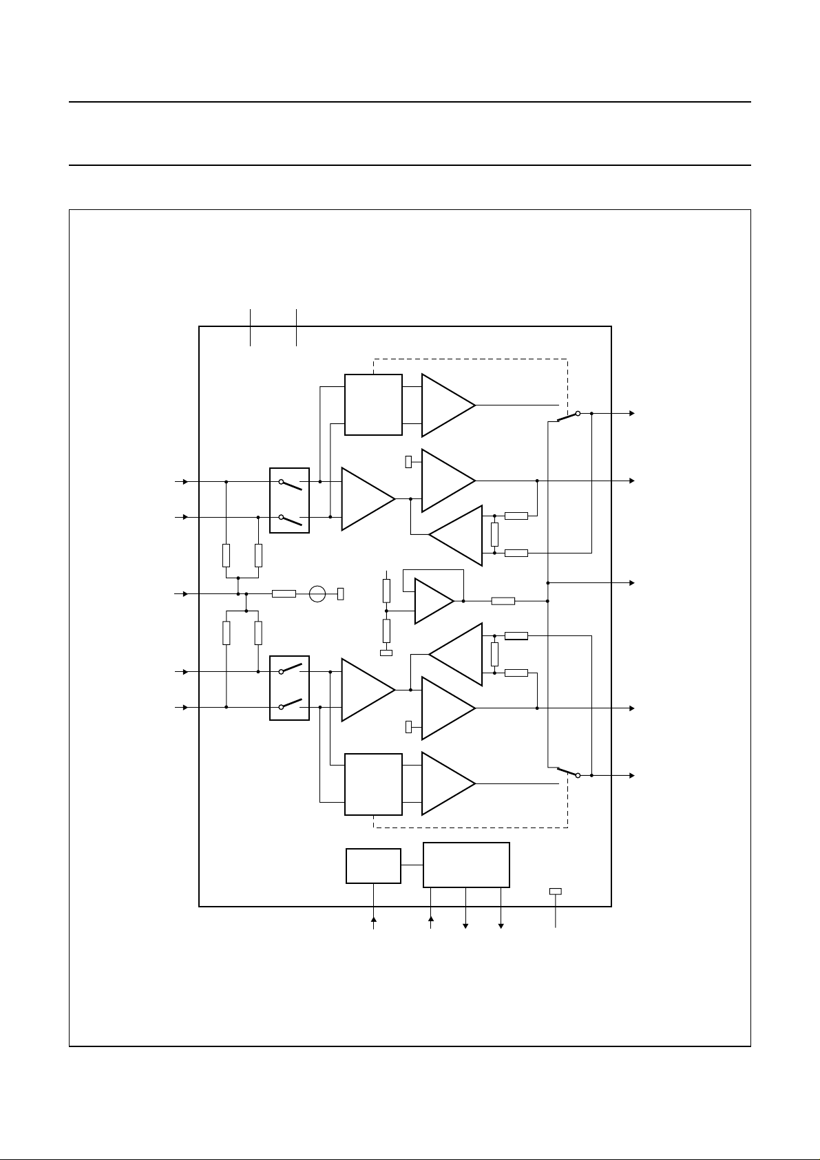
BLOCK DIAGRAM
handbook, full pagewidth
IN2−
IN2+
IN1−
IN1+
CIN
V
16
17
60
kΩ
3
60
kΩ
2
1
P1
V
P2
MUTE
13
SLAVE
CONTROL
5
−
VI
+
60
kΩ
25 kΩ
60
kΩ
V
ref
V
P
+
VI
−
MUTE
TDA1563Q
+
10
−
−
IV
+
−
VI
+
−
+
+
VI
−
+
IV
−
OUT2−
11
OUT2+
4
CSE
7
OUT1−
SLAVE
CONTROL
TDA1563Q
STANDBY
LOGIC
6121415
MODE SC DIAG CLIP
Fig.1 Block diagram.
2000 Feb 09 3
−
+
CLIP AND
DIAGNOSTIC
GND
9
MGR173
8
OUT1+
Page 4
Philips Semiconductors Product specification
2 × 25 W high efficiency car radio power
amplifier
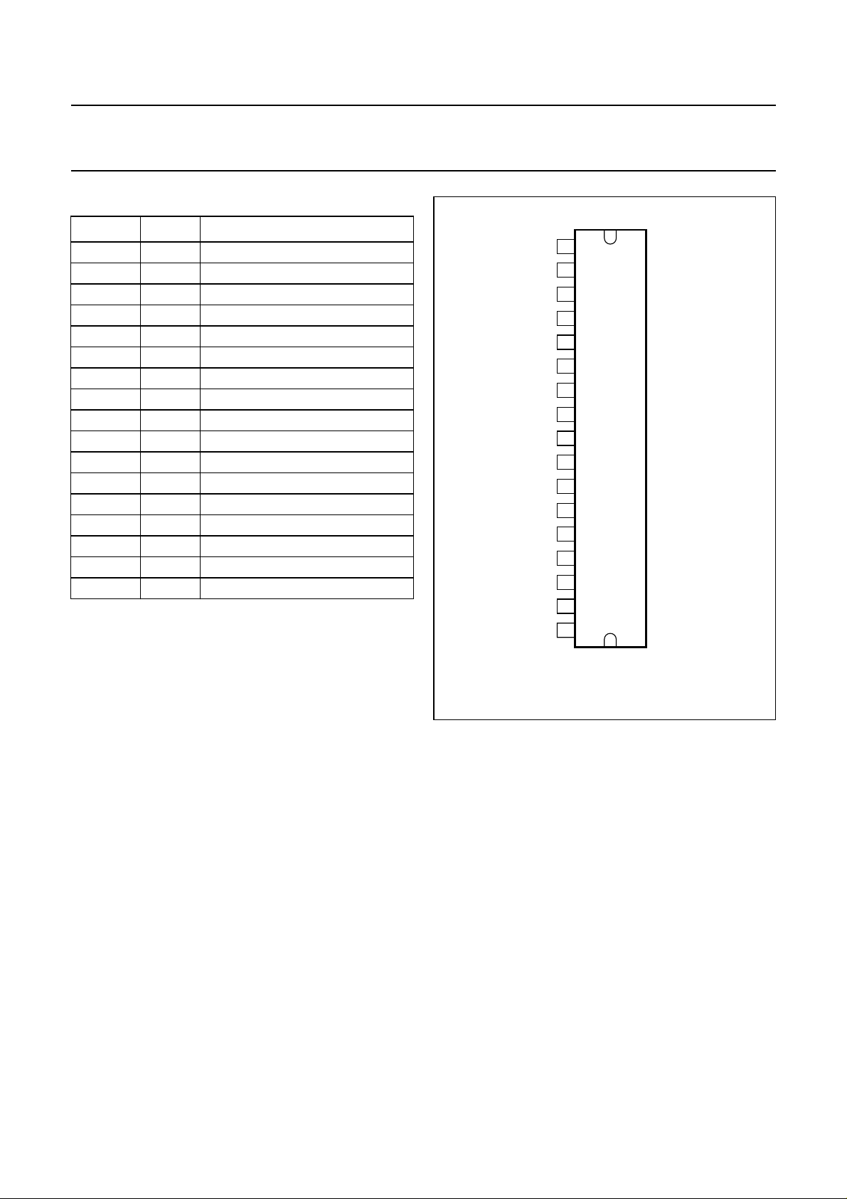
PINNING
SYMBOL PIN DESCRIPTION
IN1+ 1 non-inverting input 1
IN1− 2 inverting input 1
CIN 3 common input
CSE 4 electrolytic capacitor for SE mode
V
P1
MODE 6 mute/standby/operating
OUT1− 7 inverting output 1
OUT1+ 8 non-inverting output 1
GND 9 ground
OUT2− 10 inverting output 2
OUT2+ 11 non-inverting output 2
SC 12 selectable clip
V
P2
DIAG 14 diagnostic: protection/temperature
CLIP 15 diagnostic: clip detection
IN2− 16 inverting input 2
IN2+ 17 non-inverting input 2
5 supply voltage 1
13 supply voltage2
handbook, halfpage
IN1+
IN1−
CIN
CSE
V
P1
MODE
OUT1−
OUT1+
GND
OUT2−
OUT2+
SC
V
P2
DIAG
CLIP
IN2−
IN2+
1
2
3
4
5
6
7
8
9
TDA1563Q
10
11
12
13
14
15
16
17
TDA1563Q
MGR174
Fig.2 Pin configuration.
2000 Feb 09 4
Page 5

Philips Semiconductors Product specification
2 × 25 W high efficiency car radio power
amplifier
FUNCTIONAL DESCRIPTION
The TDA1563Q contains two identical amplifiers with
differential inputs. At low output power (up to output
amplitudes of 3 V (RMS) at VP= 14.4 V), the device
operates as a normal SE amplifier. When a larger output
voltage swing is needed, the circuit switches to BTL
operation.
With a sine wave input signal, the dissipation of a
conventionalBTL amplifier up to 2 W output power is more
than twice the dissipation of the TDA1563Q (see Fig.10).
In normal use, when the amplifier is driven with music-like
signals, the high (BTL) output power is only needed for a
smallpercentageofthetime.Assumingthatamusicsignal
has a normal (Gaussian) amplitude distribution, the
dissipation of a conventional BTL amplifier with the same
output power is approximately 70% higher (see Fig.11).
The heatsink has to be designed for use with music
signals. With such a heatsink, the thermal protection will
disable the BTL mode when the junction temperature
exceeds 150 °C.In this case, the output poweris limited to
5 W per amplifier.
The gain of each amplifier is internally fixed at 26 dB. With
the MODE pin, the device can be switched to the following
modes:
• Standby with low standby current (<50 µA)
• Mute condition, DC adjusted
• On, operation.
The information on pin 12 (selectable clip) determines at
which distortion figures a clip detection signal will be
generated at the clip output. A logic 0 applied to pin 12 will
select clip detection at THD = 10%, a logic 1 selects
THD = 2.5%. A logic 0 can be realised by connecting this
pin to ground. A logic 1 can be realised by connecting it to
V
(see Fig.7) or the pin can also be left open. Pin 12
logic
may not be connected to VP because its maximum input
voltage is 18 V (VP> 18 V under load dump conditions).
The device is fully protected against a short circuit of the
output pins to ground and to the supply voltage. It is also
protected against a short circuit of the loudspeaker and
against high junction temperatures. In the event of a
permanentshortcircuittogroundorthesupplyvoltage, the
output stage will be switched off, causing low dissipation.
With a permanent short circuit of the loudspeaker, the
output stage will be repeatedly switched on and off. In the
‘on’ condition, the duty cycle is low enough to prevent
excessive dissipation.
TDA1563Q
To avoid plops during switching from ‘mute’ to ‘on’ or from
‘on’ to ‘mute/standby’ while an input signal is present, a
built-in zero-crossing detector only allows switching at
zero input voltage. However, when the supply voltage
drops below 6 V (e.g. engine start), the circuit mutes
immediately, avoiding clicks from the electronic circuit
preceding the power amplifier.
The voltage of the SE electrolytic capacitor (pin 4) is kept
at 0.5VP by a voltage buffer (see Fig.1). The value of this
capacitor has an important influence on the output power
in SE mode. Especially at low signal frequencies, a high
value is recommended to minimize dissipation.
The two diagnostic outputs (clip and diag) are
open-collector outputs and require a pull-up resistor.
The clip output will be LOW when the THD of the output
signal is higher than the selected clip level (10% or 2.5%).
The diagnostic output gives information:
• about short circuit protection:
– When a short circuit (to ground or the supply voltage)
occurs at the outputs (for at least 10 µs), the output
stages are switched off to prevent excessive
dissipation. The outputs are switched on again
approximately 50 ms after the short circuit is
removed. During this short circuit condition, the
protection pin is LOW.
– When a short circuit occurs across the load (for at
least 10 µs), the output stages are switched off for
approximately50 ms.Afterthistime,acheckis made
to see whether the short circuit is still present.
The power dissipation in any short circuit condition is
very low.
• during startup/shutdown, when the device is internally
muted.
• temperaturedetection: This signal (junctiontemperature
> 145°C) indicates that the temperature protection will
becomeactive. The temperature detection signal can be
used to reduce the input signal and thus reduce the
power dissipation.
2000 Feb 09 5
Page 6
Philips Semiconductors Product specification
2 × 25 W high efficiency car radio power
TDA1563Q
amplifier
LIMITING VALUES
In accordance with the Absolute Maximum Rating System (IEC 134).
SYMBOL PARAMETER CONDITIONS MIN. MAX. UNIT
V
P
V
P(sc)
V
rp
I
ORM
P
tot
T
stg
T
vj
T
amb
THERMAL CHARACTERISTICS
SYMBOL PARAMETER CONDITIONS VALUE UNIT
R
th(j-c)
R
th(j-a)
supply voltage operating − 18 V
non-operating − 30 V
load dump; t
> 2.5 ms − 45 V
r
short-circuit safe voltage − 18 V
reverse polarity voltage − 6V
repetitive peak output current − 4A
total power dissipation − 60 W
storage temperature −55 +150 °C
virtual junction temperature − 150 °C
ambient temperature −40 −°C
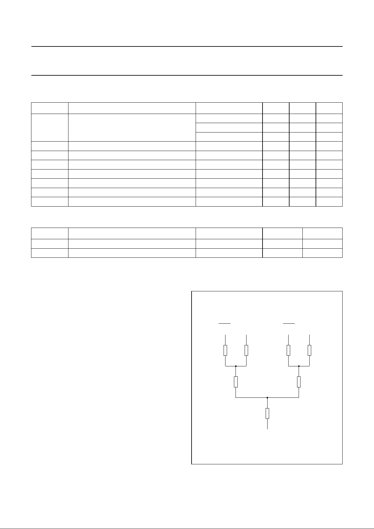
thermal resistance from junction to case see note 1 1.3 K/W
thermal resistance from junction to ambient 40 K/W
Note
1. The value of R
depends on the application (see Fig.3).
th(c-h)
Heatsink design
There are two parameters that determine the size of the
heatsink. The first is the rating for the virtual junction
temperature and the second is the ambient temperature at
which the amplifier must still deliver its full power in the
BTL mode.
With a conventional BTL amplifier, the maximum power
dissipation with a music-like signal (at each amplifier) will
be approximately two times 6.5 W.
Atavirtual junction temperature of 150 °C and a maximum
ambient temperature of 65 °C, R
R
= 0.2 K/W, the thermal resistance of the heatsink
th(c-h)
150 65–
should be:
150 65–
----------------------
---------------------2 6.5×
2 6.5×
1.3– 0.2– 5 K/W=
1.3– 0.2– 5 K/W=
= 1.3 K/W and
th(vj-c)
Comparedto a conventional BTL amplifier, the TDA1563Q
has a higher efficiency. The thermal resistance of the
145 65–
heatsink should be:
1.7
----------------------
2 6.5×
1.3– 0.2– 9 K/W=
handbook, halfpage
OUT 1 OUT 1
3.6 K/W
0.6 K/W
virtual junction
3.6 K/W
0.1 K/W
case
OUT 2 OUT 2
3.6 K/W
0.6 K/W
3.6 K/W
MGC424
2000 Feb 09 6
Fig.3 Thermal equivalent resistance network.
Page 7
Philips Semiconductors Product specification
2 × 25 W high efficiency car radio power
TDA1563Q
amplifier
DC CHARACTERISTICS
VP= 14.4 V; T
SYMBOL PARAMETER CONDITIONS MIN. TYP. MAX. UNIT
Supplies
V
P
I
q(tot)
I
stb
V
C
∆V
DC output offset voltage on state −−100 mV
O
Mode select switch (see Fig.4)
V
ms
I
ms
Diagnostic
V
diag
I
diag
V
SC
Protection
T
pre
T
dis(BTL)
=25°C; measured in Fig.7; unless otherwise specified.
amb
supply voltage note 1 6 14.4 18 V
total quiescent current RL= ∞−95 150 mA
standby current − 150µA
average electrolytic capacitor voltage at pin 4 − 7.1 − V
mute state −−100 mV
voltage at mode select pin (pin 6) standby condition 0 − 1V
mute condition 2 − 3V
operating condition 4 5 V
V
P
switch current through pin 6 Vms=5V − 25 40 µA
output voltage at diagnostic outputs (pins 14 and
during any fault condition −−0.5 V
15): protection/temperature and detection
current through pin 14 or 15 during any fault condition 2 −−mA
input voltage at selectable clip pin (pin 12) clip detect at THD = 10% −−0.5 V
clip detect at THD = 2.5% 1.5 − 18 V
prewarning temperature − 145 −°C
BTL disable temperature note 2 − 150 −°C
Notes
1. The circuit is DC biased at V
= 6 to 18 V and AC operating at VP=8to18V.
P
2. If the junction temperature exceeds 150 °C, the output power is limited to 5 W per channel.
2000 Feb 09 7
Page 8

Philips Semiconductors Product specification
2 × 25 W high efficiency car radio power
amplifier
V
18
handbook, halfpage
mode
Operating
4
3
2
1
0
Mute
Standby
MGR176
TDA1563Q
Fig.4 Switching levels of the mode select switch.
2000 Feb 09 8
Page 9

Philips Semiconductors Product specification
2 × 25 W high efficiency car radio power
TDA1563Q
amplifier
AC CHARACTERISTICS
VP= 14.4 V; RL=4Ω; CSE = 1000 µF; f = 1 kHz; T
SYMBOL PARAMETER CONDITIONS MIN. TYP. MAX. UNIT
P
o
output power THD = 0.5% 15 19 − W
THD total harmonic distortion P
P
B
f
ro(l)
f
ro(h)
G
d
p
v
dissipated power see Figs 10 and 11 W
power bandwidth THD= 1%; Po= −1dB
low frequency roll-off −1 dB; note 2 − 25 − Hz
high frequency roll-off −1dB 130 −−kHz
closed loop voltage gain Po= 1 W 25 26 27 dB
SVRR supply voltage ripple rejection R
CMRR common mode rejection ratio R
Z
input impedance 90 120 150 kΩ
i
∆Z
mismatch in input impedance − 1 − %
i
V
SE-BTL
V
o(mute)
V
n(o)
α
cs
∆G
SE to BTL switch voltage level note 3 − 3 − V
output voltage mute (RMS value) Vi= 1 V (RMS) − 100 150 µV
noise output voltage on; Rs=0Ω; note 4 − 100 150 µV
channel separation Rs=0Ω; Po=15W 40 70 − dB
channel unbalance −− 1dB
v
=25°C; measured in Fig.7; unless otherwise specified.
amb
THD = 10% 23 25 − W
EIAJ − 38 − W
V
= 13.2 V; THD = 0.5% − 16 − W
P
V
= 13.2 V; THD = 10% − 20 − W
P
= 1 W; note 1 − 0.1 − %
o
− 20 to 15000 − Hz
with respect to 15 W
=0Ω; V
s
ripple
= 2 V (p-p)
on/mute 45 65 − dB
standby; f = 100 Hz to 10 kHz 80 −−dB
=0Ω−80 − dB
s
on; R
=10kΩ; note 4 − 105 −µV
s
mute; note 5 − 100 150 µV
Notes
1. The distortion is measured with a bandwidth of 10 Hz to 30 kHz.
2. Frequency response externally fixed (input capacitors determine low frequency roll-off).
3. The SE to BTL switch voltage level depends on V
.
P
4. Noise output voltage measured with a bandwidth of 20 Hz to 20 kHz.
5. Noise output voltage is independent of Rs.
2000 Feb 09 9
Page 10
Philips Semiconductors Product specification
2 × 25 W high efficiency car radio power
amplifier
handbook, halfpage
V
o
0
CLIP
0
MGR177
t
handbook, halfpage
I
o
max
max
DIAG
0
TDA1563Q
10 µs
short circuit
removed
short circuit
to ground
50
ms
maximum current short circuit to supply pins
50
ms
50
ms
MGR178
t
t
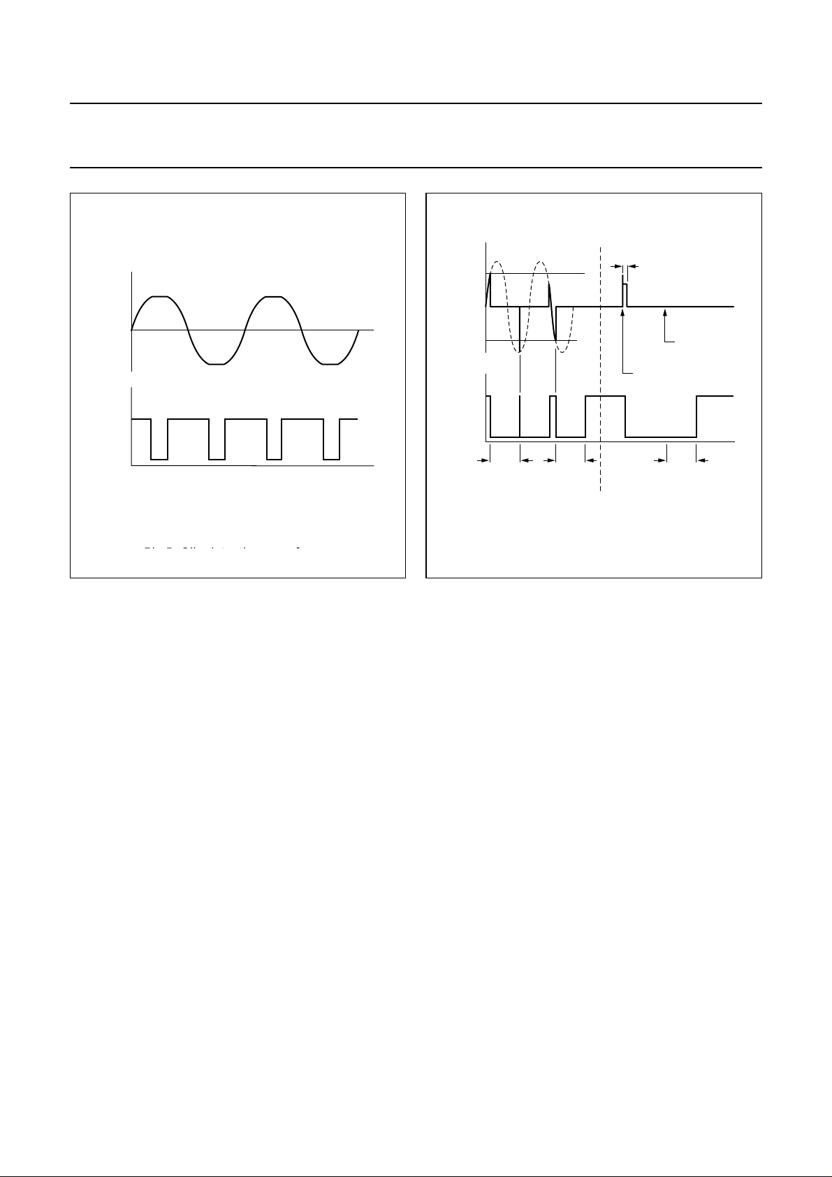
Fig.5 Clip detection waveforms.
Fig.5 Clip detection waveforms. Fig.6 Protection waveforms.
2000 Feb 09 10
Page 11

Philips Semiconductors Product specification
2 × 25 W high efficiency car radio power
amplifier
TEST AND APPLICATION INFORMATION
handbook, full pagewidth
V
P1
5
TDA1563Q
−
0.5R
1 µF
0.5R
s
220 nF
s
220 nF
16IN2−
17IN2+
3CIN
60kΩ60
25 kΩ
+
−
+
kΩ
TDA1563Q
3.9 Ω
V
P
V
P2
13
10
11
V
ref
4
220 nF 2200 µF
OUT2−
4 Ω
OUT2+
CSE
1000 µF
100 nF
100 nF
Ω
3.9
0.5R
0.5R
s
220 nF
s
220 nF
60kΩ60
2IN1−
kΩ
+
−
1IN1+
+
−
ms
CLIP AND
DIAGNOSTIC
STANDBY
LOGIC
6121415
MODE SC DIAG CLIP9GND
V
2.5%
10%
R
R
7
8
pu
pu
OUT1−
4 Ω
OUT1+
V
logic
MGR180
Ω
3.9
100 nF
3.9 Ω
100 nF
signal ground
power ground
Connect Boucherot filter to pin 8 or pin 10 with the shortest possible connection.
Fig.7 Application diagram.
2000 Feb 09 11
Page 12

Philips Semiconductors Product specification
2 × 25 W high efficiency car radio power
amplifier
handbook, full pagewidth
76.20
TDA1563Q
35.56
+
Out2
−
RL-98
2.5%
−
Dimensions in mm.
gnd
In1
+
Mode
On
Off
10%
Mute
Clip
Vp
Fig.8 PCB layout (component side) for the application of Fig.7.
2000 Feb 09 12
GND
Prot
Clip
TDA1563Q
−
Out2
+
−
In2
+
gnd
MGR189
Page 13

Philips Semiconductors Product specification
2 × 25 W high efficiency car radio power
amplifier
handbook, full pagewidth
76.20
TDA1563Q
35.56
Dimensions in mm.
2× 25 W high efficiency
Out1
In1
MGR190
In2
Out2
220 nF
17
GND
220 nF
1
1 µF
220 nF
Vp
Fig.9 PCB layout (soldering side) for the application of Fig.7.
2000 Feb 09 13
Page 14

Philips Semiconductors Product specification
2 × 25 W high efficiency car radio power
amplifier
25
handbook, halfpage
P
d
(W)
20
15
10
5
0
010
Input signal 1 kHz, sinusoidal; VP= 14.4 V.
(1) For a conventional BTL amplifier.
(2) For TDA1563Q.
(1)
(2)
2
468
Fig.10 Dissipation; sine wave driven.
MBH692
P
(W)
o
TDA1563Q
25
handbook, halfpage
P
d
(W)
20
(1)
15
10
5
0
010
(1) For a conventional BTL amplifier.
(2) For TDA1563Q.
(2)
2
468
Fig.11 Dissipation; pink noise through IEC-268
filter.
MBH693
P
o
(W)
430 Ω
input output
3.3
kΩ
91
nF
330 Ω
Fig.12 IEC-268 filter.
2000 Feb 09 14
3.3
kΩ
68
nF
470 nF2.2 µF 2.2 µF
10
kΩ
MGC428
Page 15

Philips Semiconductors Product specification
2 × 25 W high efficiency car radio power
amplifier
handbook, full pagewidth
TDA1563Q
16IN2−
220 nF
17IN2+
pink
noise
220 nF
1 µF
IEC-268
FILTER
220 nF
220 nF
3CIN
2IN1−
1IN1+
60kΩ60
60kΩ60
kΩ
25 kΩ
kΩ
TDA1563Q
3.9
3.9
V
P
Ω
Ω
P1
V
P2
13
V
5
220 nF 2200 µF
−
10
OUT2−
100 nF
+
100 nF
4
Ω
−
11
OUT2+
3.9
Ω
+
V
ref
+
−
+
−
4
7
8
CSE
OUT1−
4
OUT1+
1000 µF
Ω
Ω
3.9
100 nF
100 nF
STANDBY
LOGIC
6121415
MODE SC DIAG CLIP
V
ms
Fig.13 Test and application diagram for dissipation measurements with a music-like signal (pink noise).
2000 Feb 09 15
CLIP AND
DIAGNOSTIC
9
GND
R
pu
R
pu
V
signal ground
power ground
logic
MGR181
Page 16

Philips Semiconductors Product specification
2 × 25 W high efficiency car radio power
amplifier
Vp (V)
MDA845
2416
150
handbook, halfpage
I
q
(mA)
100
50
0
0
8
250
handbook, halfpage
I
p
(mA)
200
150
100
50
0
02
TDA1563Q
MDA844
46
V
(V)
ms
Vms= 5 V; RI= ∞.
Fig.14 Quiescent current as a function of VP.
60
handbook, halfpage
P
o
(W)
40
20
0
818
10
12 14 16
(1)
(2)
(3)
MDA843
Vp (V)
VP= 14.4 V; Vi=25mV
Fig.15 IP as a function of Vms (pin 3).
10
handbook, halfpage
THD + N
(%)
1
−1
10
−2
10
−2
10
MDA842
(1)
(2)
(3)
−1
10
1
10
Po (W)
2
10
(1) EIAJ, 100 Hz.
(2) THD = 10 %.
(3) THD = 0.5 %.
Fig.16 Output power as a function of VP.
2000 Feb 09 16
(1) f = 10 kHz.
(2) f = 1 kHz.
(3) f = 100 Hz.
Fig.17 THD + noise as a function of Po.
Page 17

Philips Semiconductors Product specification
2 × 25 W high efficiency car radio power
amplifier
10
handbook, halfpage
THD + N
(%)
1
−1
10
−2
10
10 10
2
3
10
MDA841
(1)
(2)
f (Hz)
5
10
4
10
28
handbook, halfpage
G
v
(dB)
26
24
22
20
10 10
TDA1563Q
MDA840
2
3
10
4
10
5
10
f (Hz)
6
10
(1) Po=10W.
(2) Po=1W.
Fig.18 THD + noise as a function of frequency.
−10
handbook, halfpage
α
cs
(dB)
−30
−50
−70
−90
10
(1)
(2)
2
10
3
10
4
10
f (Hz)
MDA838
Vi= 100 mV.
Fig.19 Gain as a function of frequency.
MDA839
4
10
f (Hz)
5
10
SVRR
(dB)
0
handbook, halfpage
−20
−40
−60
5
10
−80
10
2
10
3
10
(1) Po=10W.
(2) Po=1W.
Fig.20 Channel separation as a function of
frequency.
2000 Feb 09 17
V
ripple(p-p)
=2V.
Fig.21 SVRR as a function of frequency.
Page 18

Philips Semiconductors Product specification
2 × 25 W high efficiency car radio power
amplifier
0.8
handbook, halfpage
P
o
(W)
0.6
0.4
0.2
0
08
16
MDA846
V
24
(V)
p
TDA1563Q
Vi=70mV.
Fig.22 AC operating as a function of VP.
2000 Feb 09 18
Page 19

Philips Semiconductors Product specification
2 × 25 W high efficiency car radio power
amplifier
handbook, full pagewidth
V
load
V
P
0
TDA1563Q
MGL914
See Fig.7:
V
load=V7−V8
V
master=V7
V
slave=V8
or V11− V
or V
or V
10
−V
P
V
P
V
master
1/2 V
P
0
V
P
V
slave
1/2 V
P
0
0 1 2 t (ms) 3
10
11
Fig.23 Output waveforms.
2000 Feb 09 19
Page 20

Philips Semiconductors Product specification
2 × 25 W high efficiency car radio power
amplifier
APPLICATION NOTES
Example of the TDA1563Q in a car radio system
solution
The PCB shown here is used to demonstrate an audio
system solution with Philips Semiconductors devices for
caraudio applications. The board includes the SAA7705H:
a high-end CarDSP (Digital Signal Processor), the
TDA3617J: a voltage regulator providing 9 V, 5 V and
3.3 V outputs, and two TDA1563Qs to provide four 25 W
power outputs. A complete kit (application report, software
and demo board) of this “car-audio chip-set demonstrator”
is available.
The TDA1563Q is a state of the art device, which is
different to conventional amplifiers in power dissipation
because it switches between SE mode and conventional
BTL mode, depending on the required output voltage
swing. As a result, the PCBlayout is more critical than with
conventional amplifiers.
NOTES AND LAYOUT DESIGN RECOMMENDATIONS
1. The TDA1563Q mutes automatically during switch-on
and switch-off and suppresses biasing clicks coming
fromthe CarDSP circuit preceding the power amplifier.
Therefore, it is not necessary to use a plop reduction
circuit for the CarDSP. To mute or to enlarge the mute
time of the system, the voltage at the mode pin of the
amplifiers should be kept between 2 V and 3 V.
2. The input reference capacitor at pin 3 is specified as
1 µF but has been increased to 10 µF to improve the
switch-onplopperformance of the amplifiers. By doing
this, the minimum switch-on time increases from
standby,viainternalmute,tooperatingfrom150 ms to
600 ms.
3. It is important that the copper tracks to and from the
electrolytic capacitors (SE capacitors and supply
capacitors) are close together. Because of the
switching principle, switching currents flow here.
Combining electrolytic capacitors in a 4-channel
application is not recommended.
4. Filters at the outputs are necessary for stability
reasons. The filters at output pins 8 and 10 to ground
should be connected as close as possible to the
device (see layout of PCB).
TDA1563Q
5. Connect the supply decoupling capacitors of 220 nF
as closely as possible to the TDA1563Qs.
6. Place the tracks of the differential inputs as close
togetheras possible. If disturbances are injected at the
inputs, they will be amplified 20 times. Oscillation may
occur if this is not done properly.
7. The SE line output signal of the CarDSP here is
offered as a quasi differential input signal to the
amplifiers by splitting the 100 Ω unbalance series
resistance into two 47 Ω balanced series resistances.
Thereturntrackfrom the minus inputs of the amplifiers
are not connected to ground (plane) but to the line out
reference voltage of the CarDSP, VrefDA.
8. The output signal of the CarDSP needs an additional
1st order filter. This is done by the two balanced series
resistances of 47 Ω (see note 7) and a ceramic
capacitor of 10 nF. The best position to place these
10 nF capacitors is directly on the input pins of the
amplifiers.Now,any high frequency disturbance at the
inputs of the amplifiers will be rejected.
9. Only the area underneath the CarDSP is a ground
plane. A ground plane is necessary in PCB areas
where high frequency digital noise occurs. The audio
outputs are low frequency signals. For these outputs,
itis better to use two tracks (feed and return)asclosely
as possible to each other to make the disturbances
common mode. The amplifiers have differential inputs
with a very high common mode rejection.
10. The ground pin of the voltage regulator is the
reference for the regulator outputs. This ground
reference should be connected to the ground plane of
the CarDSP by one single track. The ground plane of
theCarDSP may not be connectedto“another” ground
by a second connection.
11. Prevent power currents from flowing through the
ground connection between CarDSP and voltage
regulator. The currents in the ground from the
amplifiers are directly returned to the ground pin of the
demo board. By doing this so, no ground interference
between the components will occur.
2000 Feb 09 20
Page 21

Philips Semiconductors Product specification
2 × 25 W high efficiency car radio power
amplifier
handbook, full pagewidth
Line-in
Left
(3)
Car-audio chip-set demonstrator
+
2.5%
10%
Car DSP
SAA7704/05/08
on bottom side
V
BATT
IO-98
+
(3)
TDA1563QTDA1563QTDA3617J
Error On
FrontRear
Diag Clip
TDA1563Q
−
FL
+
−
RL
+
10 V to 16 V
V
battery
FR
RR
+
−
+
−
Right
PHILIPS Semiconductors
(4)
4× 25 W into 4 Ohms
(5)
Power ON Mute
2
I
C
Top copper layer
(8)
Car-audio chip-set demonstrator
Version 0.1
DSP
GND
(6)
Bottom copper layer
Fig.24 PCB layout.
2000 Feb 09 21
MGS827
Page 22

Philips Semiconductors Product specification
2 × 25 W high efficiency car radio power
amplifier
handbook, full pagewidth
V
LEFT
LINE
IN
RIGHT
CD-GND
I2C
SCL
SDA
MICROCONTROLLER
BATT
power
4.7 kΩ
error
mute
4.7 kΩ
diagnostic
4.7 kΩ
clip
1 µF
15 kΩ
1 µF
15 kΩ
1 µF
47 nF
PLANE
1 to 5
PLANE
6
5 V
8
7
100 Ω
100 µF
GND
3.3 V ANA
330 pF
8.2 kΩ
330 pF
8.2 kΩ
1 MΩ
82 kΩ
22 µF
4.7 kΩ
power
on
VDACN1
PLANE
VREFAD
VDACP
CDLB
CDLI
CDRB
CDRI
CDGND
AMAFR
AMAFL
TAPER
TAPEL
1
2
73
72
71
70
77
78
66
67
68
69
100 nF
DDA1
V
74
4 3
AML
BLM21A10
FML
PLANE
47 µF
SSA1
V
75
61
SELFR
3.3 V DIG
PLANE
VDACN2
76
65
DD(OSC)
V
100 nF
GND
GND
TP522V
21
VOLTAGE REGULATOR
V
en1
2
V
en3
1
6
REG2
47 nF
5 V 3.3 V DIG 3.3 V ANA
22 nF
PLANE
DDD5V1
SSD5V1
V
23
63
62
OSCIN
SS(OSC)
V
X1
PLANE
18
pF
PLANE
TDA3617J
9
HOLD7V
en2
5 V
100 Ω
22 nF
PLANE
DDD5V2
SSD5V2
V
V
36
37
Car DSP
SAA7704/05/08H
42
64
OSCOUT
DSPRESET
220 nF
220
PLANE
100
18
pF
pF
PLANE
PLANE
5
22 nF
DDD5V3
V
46
57
SCL
Ω
REG3
3
8
PLANE
SSD5V3
V
47
58
SDA
220
Ω
PLANE
V
P
GND
47 µF
V
56A024
3.3 V DIG
DDD3V1
V
48
51
CD2WS
100 pF
220 nF
GND
BLM21A10
DDD3V2
DDD3V3
V
52
25
CD2DATA
PLANE GND
47 nF
100 nF
DDD3V4
SSD3V1
V
V
55
49
26
27
28
CD2CL
CD1WS
CD1DATA
PLANE
V
BATT
SSD3V2
V
V
50
53
29
CD1CL
BAS16/A6
1 MΩ
PLANE
SSD3V3
SSD3V4
V
54
43
44
RTCB
SHTCB
DDA2
V
11
16
15
13
14
12
10
45
TSCAN
TDA1563Q
5 V
10 kΩ
10 kΩ
BC848B/1k
GND
3.3 V ANA
100 nF
PLANE
FLV
2.2
nF
FLI
FRV
2.2
nF
FRI
RRV
6
7
9
8
RRI
RLV
RLI
VREFDA
V
SSA2
PLANE
MGS825
2.2
nF
2.2
nF
22 µF
47 Ω
47 Ω
47 Ω
47 Ω
47 Ω
47 Ω
47 Ω
47 Ω
A
B
C
D
E
F
G
H
I
J
K
Fig.25 Car-audio chip-set demonstrator (continued in Fig.26).
2000 Feb 09 22
Page 23

Philips Semiconductors Product specification
2 × 25 W high efficiency car radio power
amplifier
handbook, full pagewidth
A
2.5%
10%
220 nF
220 nF
220 nF
220 nF
10 µF
10 µF
220 nF
220 nF
220 nF
220 nF
GND
5 V
10 nF
10 nF
10 nF
10 nF
BATT
MODE
PGND
MODE
BATT
CLIP
DIAG
IN2+
IN2−
IN1+
IN1−
IN1+
IN1−
IN2+
IN2−
DIAG
CLIP
SC
CIN
CIN
SC
clip select
B
C
D
E
F
G
H
I
J
K
V
V
P1
13
5
15
14
12
17
TDA1563Q
16
1
2
3
BATT
2200 µF
(16 V)
220 nF
V
P2
GND PGND
GND
9
CSE
46
OUT2+
11
OUT2−
10
OUT1+
8
OUT1−
7
100 µH/6A
PGNDV
1000 µF
3.9 Ω
3.9 Ω
(16 V)
3.9 Ω
100 nF
100 nF
100 nF
3.9 Ω
100 nF
V battery
GND
PGND
PGND
2× HIGH EFFICIENCY POWER AMPLIFIER
OUT1−
P1
13
V
2200 µF
(16 V)
P2
220 nF
7
OUT1+
8
OUT2−
10
OUT2+
11
CSE
46
9
GND
PGNDV
3.9 Ω
3.9 Ω
1000 µF
(16 V)
3.9 Ω
100 nF
100 nF
100 nF
100 nF
3.9 Ω
PGND
PGND
3
1
2
17
TDA1563Q
16
12
14
15
5
V
OUT+
FRONT
LEFT
OUT−
OUT+
FRONT
RIGHT
OUT−
OUT−
REAR
RIGHT
OUT+
OUT−
REAR
LEFT
OUT+
MGS826
TDA1563Q
Fig.26 Car-audio chip-set demonstrator (continued from Fig.25).
2000 Feb 09 23
Page 24

Philips Semiconductors Product specification
2 × 25 W high efficiency car radio power
amplifier
Advantages of high efficiency
• Power conversion improvement (power supply)
Usually, the fact that the reduction of dissipation is
directly related to supply current reduction is neglected.
One advantage is less voltage drop in the whole supply
chain.Another advantage is less stress for the coil inthe
supply line. Even the adapter or supply circuit remains
cooler than before as a result of the reduced heat
dissipation in the whole chain because more supply
current will be converted to output power.
• Power dissipation reduction
This is the best known advantage of high efficiency
amplifiers.
• Heatsink size reduction
The heatsink size of a conventional amplifier may be
reduced by approximately 50% at VP= 14.4 V when the
TDA1563Q is used. In this case, the maximum heatsink
temperature will remain the same.
• Heatsink temperature reduction
The power dissipation and the thermal resistance of the
heatsinkdetermine the heatsink temperature rise. When
the same heatsink size is used as in a conventional
amplifier, the maximum heatsink temperature
decreases and also the maximum junction temperature,
which extends the life of this semiconductor device.
The maximum dissipation with music-like input signals
decreases by 40%.
It is clear that the use of the TDA1563Q saves a significant
amount of energy. The maximum supply current
decreases by approximately 32%, which reduces the
dissipation in the amplifier as well in the whole supply
chain. The TDA1563Q allows a heatsink size reduction of
approximately 50% or a heatsink temperature decrease of
40% when the heatsink size is not changed.
TDA1563Q
handbook, halfpage
Same junction
temperature
Heatsink
size
reduction of
50%
Advantage of the concept used by the TDA1563Q
The TDA1563Q is highly efficient under all conditions,
because it uses a SE capacitor to create a non-dissipating
half supply voltage. Other concepts rely on both input
signals being the same in amplitude and phase. With the
concept of an SE capacitor, it does not matter what kind of
signal processing is done on the input signals.
For example, amplitude difference, phase shift or delays
betweenboth input signals, or other DSP processing,have
no impact on the efficiency.
VP = 14.4 V
dissipation
Supply
current
reduction of
32%
choice
reduction of 40%
at Po = 1.6 W
Same heatsink
Heatsink
temperature
reduction of
40%
Fig.27 Heatsink design
Power
size
MGS824
2000 Feb 09 24
Page 25

Philips Semiconductors Product specification
2 × 25 W high efficiency car radio power
amplifier
INTERNAL PIN CONFIGURATIONS
PIN NAME EQUIVALENT CIRCUIT
1, 2, 16,
17 and 3
4C
IN1+, IN1−, IN2−,
IN2+ and CIN
SE
1, 2, 16, 17
V
P1, VP2
V
P1
V
P2
V
P1, VP2
TDA1563Q
3
MGR182
6 MODE
7, 11 OUT1−, OUT2+
6
V
P1, VP2
4
MGR183
MGR184
2000 Feb 09 25
7, 11
4
MGR185
Page 26

Philips Semiconductors Product specification
2 × 25 W high efficiency car radio power
amplifier
PIN NAME EQUIVALENT CIRCUIT
8, 10 OUT1+, OUT2−
12 SC
V
P1, VP2
V
P2
12
TDA1563Q
8, 10
4
MGR186
14, 15 PROT, CLIP
MGR187
V
P2
14, 15
MGR188
2000 Feb 09 26
Page 27

Philips Semiconductors Product specification
2 × 25 W high efficiency car radio power
amplifier
PACKAGE OUTLINE
DBS17P: plastic DIL-bent-SIL power package; 17 leads (lead length 12 mm)
non-concave
D
d
x
E
h
D
h
view B: mounting base side
A
2
TDA1563Q
SOT243-1
117
e
Z
DIMENSIONS (mm are the original dimensions)
UNIT A e
mm
A2bpcD
17.0
4.6
4.4
0.75
0.60
15.5
0.48
0.38
1
e
(1)
deD
24.0
20.0
23.6
19.6
w M
b
p
(1)
E
h
12.2
10 2.54
11.8
0 5 10 mm
B
j
L
3
1.27
scale
1
e
5.08
L
E
2
h
6
Q
LL3m
3.4
12.4
3.1
11.0
2.4
1.6
e
4.3
m
E
A
c
2
2.1
1.8
v M
(1)
v
Qj
0.8
0.4w0.03
Z
x
2.00
1.45
Note
1. Plastic or metal protrusions of 0.25 mm maximum per side are not included.
OUTLINE
VERSION
SOT243-1
IEC JEDEC EIAJ
REFERENCES
2000 Feb 09 27
EUROPEAN
PROJECTION
ISSUE DATE
97-12-16
99-12-17
Page 28

Philips Semiconductors Product specification
2 × 25 W high efficiency car radio power
amplifier
SOLDERING
Introduction to soldering through-hole mount
packages
This text gives a brief insight to wave, dip and manual
soldering.Amorein-depthaccountofsolderingICscanbe
found in our
Packages”
Wave soldering is the preferred method for mounting of
through-hole mount IC packages on a printed-circuit
board.
Soldering by dipping or by solder wave
The maximum permissible temperature of the solder is
260 °C; solder at this temperature must not be in contact
with the joints for more than 5 seconds.
Suitability of through-hole mount IC packages for dipping and wave soldering methods
DBS, DIP, HDIP, SDIP, SIL suitable suitable
“Data Handbook IC26; Integrated Circuit
(document order number 9398 652 90011).
PACKAGE
Thetotal contact time of successive solder waves must not
exceed 5 seconds.
The device may be mounted up to the seating plane, but
the temperature of the plastic body must not exceed the
specified maximum storage temperature (T
printed-circuit board has been pre-heated, forced cooling
may be necessary immediately after soldering to keep the
temperature within the permissible limit.
Manual soldering
Apply the soldering iron (24 V or less) to the lead(s) of the
package, either below the seating plane or not more than
2 mm above it. If the temperature of the soldering iron bit
is less than 300 °C it may remain in contact for up to
10 seconds. If the bit temperature is between
300 and 400 °C, contact may be up to 5 seconds.
SOLDERING METHOD
DIPPING WAVE
(1)
TDA1563Q
). If the
stg(max)
Note
1. For SDIP packages, the longitudinal axis must be parallel to the transport direction of the printed-circuit board.
DEFINITIONS
Data sheet status
Objective specification This data sheet contains target or goal specifications for product development.
Preliminary specification This data sheet contains preliminary data; supplementary data may be published later.
Product specification This data sheet contains final product specifications.
Limiting values
Limiting values given are in accordance with the Absolute Maximum Rating System (IEC 134). Stress above one or
more of the limiting values may cause permanent damage to the device. These are stress ratings only and operation
of the device at these or at any other conditions above those given in the Characteristics sections of the specification
is not implied. Exposure to limiting values for extended periods may affect device reliability.
Application information
Where application information is given, it is advisory and does not form part of the specification.
LIFE SUPPORT APPLICATIONS
These products are not designed for use in life support appliances, devices, or systems where malfunction of these
products can reasonably be expected to result in personal injury. Philips customers using or selling these products for
use in such applications do so at their own risk and agree to fully indemnify Philips for any damages resulting from such
improper use or sale.
2000 Feb 09 28
Page 29

Philips Semiconductors Product specification
2 × 25 W high efficiency car radio power
amplifier
NOTES
TDA1563Q
2000 Feb 09 29
Page 30

Philips Semiconductors Product specification
2 × 25 W high efficiency car radio power
amplifier
NOTES
TDA1563Q
2000 Feb 09 30
Page 31

Philips Semiconductors Product specification
2 × 25 W high efficiency car radio power
amplifier
NOTES
TDA1563Q
2000 Feb 09 31
Page 32

Philips Semiconductors – a w orldwide compan y
Argentina: see South America
Australia: 3 Figtree Drive, HOMEBUSH, NSW 2140,
Tel. +61 2 9704 8141, Fax. +61 2 9704 8139
Austria: Computerstr. 6, A-1101 WIEN, P.O. Box 213,
Tel. +43 1 60 101 1248, Fax. +43 1 60 101 1210
Belarus: Hotel Minsk Business Center, Bld. 3, r. 1211, Volodarski Str. 6,
220050 MINSK, Tel. +375 172 20 0733, Fax. +375 172 20 0773
Belgium: see The Netherlands
Brazil: see South America
Bulgaria: Philips Bulgaria Ltd., Energoproject, 15th floor,
51 James Bourchier Blvd., 1407 SOFIA,
Tel. +359 2 68 9211, Fax. +359 2 68 9102
Canada: PHILIPS SEMICONDUCTORS/COMPONENTS,
Tel. +1 800 234 7381, Fax. +1 800 943 0087
China/Hong Kong: 501 Hong Kong Industrial Technology Centre,
72 Tat Chee Avenue, Kowloon Tong, HONG KONG,
Tel. +852 2319 7888, Fax. +852 2319 7700
Colombia: see South America
Czech Republic: see Austria
Denmark: Sydhavnsgade 23, 1780 COPENHAGEN V,
Tel. +45 33 29 3333, Fax. +45 33 29 3905
Finland: Sinikalliontie 3, FIN-02630 ESPOO,
Tel. +358 9 615 800, Fax. +358 9 6158 0920
France: 51 Rue Carnot, BP317, 92156 SURESNES Cedex,
Tel. +33 1 4099 6161, Fax. +33 1 4099 6427
Germany: Hammerbrookstraße 69, D-20097 HAMBURG,
Tel. +49 40 2353 60, Fax. +49 40 2353 6300
Hungary: see Austria
India: Philips INDIA Ltd, Band Box Building, 2nd floor,
254-D, Dr. Annie Besant Road, Worli, MUMBAI 400 025,
Tel. +91 22 493 8541, Fax. +91 22 493 0966
Indonesia: PT Philips Development Corporation, Semiconductors Division,
Gedung Philips, Jl. Buncit Raya Kav.99-100, JAKARTA 12510,
Tel. +62 21 794 0040 ext. 2501, Fax. +62 21 794 0080
Ireland: Newstead, Clonskeagh, DUBLIN 14,
Tel. +353 1 7640 000, Fax. +353 1 7640 200
Israel: RAPAC Electronics, 7 Kehilat Saloniki St, PO Box 18053,
TEL AVIV 61180, Tel. +972 3 645 0444, Fax. +972 3 649 1007
Italy: PHILIPS SEMICONDUCTORS, Via Casati, 23 - 20052 MONZA (MI),
Tel. +39 039 203 6838, Fax +39 039 203 6800
Japan: Philips Bldg 13-37, Kohnan 2-chome, Minato-ku,
TOKYO 108-8507, Tel. +81 3 3740 5130, Fax. +81 3 3740 5057
Korea: Philips House, 260-199 Itaewon-dong, Yongsan-ku, SEOUL,
Tel. +82 2 709 1412, Fax. +82 2 709 1415
Malaysia: No. 76 Jalan Universiti, 46200 PETALING JAYA, SELANGOR,
Tel. +60 3 750 5214, Fax. +60 3 757 4880
Mexico: 5900 Gateway East, Suite 200, EL PASO, TEXAS 79905,
Tel. +9-5 800 234 7381, Fax +9-5 800 943 0087
Middle East: see Italy
Netherlands: Postbus 90050, 5600 PB EINDHOVEN, Bldg. VB,
Tel. +31 40 27 82785, Fax. +31 40 27 88399
New Zealand: 2 Wagener Place, C.P.O. Box 1041, AUCKLAND,
Tel. +64 9 849 4160, Fax. +64 9 849 7811
Norway: Box 1, Manglerud 0612, OSLO,
Tel. +47 22 74 8000, Fax. +47 22 74 8341
Pakistan: see Singapore
Philippines: Philips Semiconductors Philippines Inc.,
106 Valero St. Salcedo Village, P.O. Box 2108 MCC, MAKATI,
Metro MANILA, Tel. +63 2 816 6380, Fax. +63 2 817 3474
Poland: Al.Jerozolimskie 195 B, 02-222 WARSAW,
Tel. +48 22 5710 000, Fax. +48 22 5710 001
Portugal: see Spain
Romania: see Italy
Russia: Philips Russia, Ul. Usatcheva 35A, 119048 MOSCOW,
Tel. +7 095 755 6918, Fax. +7 095 755 6919
Singapore: Lorong 1, Toa Payoh, SINGAPORE 319762,
Tel. +65 350 2538, Fax. +65 251 6500
Slovakia: see Austria
Slovenia: see Italy
South Africa: S.A. PHILIPS Pty Ltd., 195-215 Main Road Martindale,
2092 JOHANNESBURG, P.O. Box 58088 Newville 2114,
Tel. +27 11 471 5401, Fax. +27 11 471 5398
South America: Al. Vicente Pinzon, 173, 6th floor,
04547-130 SÃO PAULO, SP, Brazil,
Tel. +55 11 821 2333, Fax. +55 11 821 2382
Spain: Balmes 22, 08007 BARCELONA,
Tel. +34 93 301 6312, Fax. +34 93 301 4107
Sweden: Kottbygatan 7, Akalla, S-16485 STOCKHOLM,
Tel. +46 8 5985 2000, Fax. +46 8 5985 2745
Switzerland: Allmendstrasse 140, CH-8027 ZÜRICH,
Tel. +41 1 488 2741 Fax. +41 1 488 3263
Taiwan: Philips Semiconductors, 6F, No. 96, Chien Kuo N. Rd., Sec. 1,
TAIPEI, Taiwan Tel. +886 2 2134 2886, Fax. +886 2 2134 2874
Thailand: PHILIPS ELECTRONICS (THAILAND) Ltd.,
209/2 Sanpavuth-Bangna Road Prakanong, BANGKOK 10260,
Tel. +66 2 745 4090, Fax. +66 2 398 0793
Turkey: Yukari Dudullu, Org. San. Blg., 2.Cad. Nr. 28 81260 Umraniye,
ISTANBUL, Tel. +90 216 522 1500, Fax. +90 216 522 1813
Ukraine: PHILIPS UKRAINE, 4 Patrice Lumumba str., Building B, Floor 7,
252042 KIEV, Tel. +380 44 264 2776, Fax. +380 44 268 0461
United Kingdom: Philips Semiconductors Ltd., 276 Bath Road, Hayes,
MIDDLESEX UB3 5BX, Tel. +44 208 730 5000, Fax. +44 208 754 8421
United States: 811 East Arques Avenue, SUNNYVALE, CA 94088-3409,
Tel. +1 800 234 7381, Fax. +1 800 943 0087
Uruguay: see South America
Vietnam: see Singapore
Yugoslavia: PHILIPS, Trg N. Pasica 5/v, 11000 BEOGRAD,
Tel. +381 11 3341 299, Fax.+381 11 3342 553
For all other countries apply to: Philips Semiconductors,
International Marketing & Sales Communications, Building BE-p, P.O. Box 218,
5600 MD EINDHOVEN, The Netherlands, Fax. +31 40 27 24825
© Philips Electronics N.V. SCA
All rights are reserved. Reproduction in whole or in part is prohibited without the prior written consent of the copyright owner.
The information presented in this document does not form part of any quotation or contract, is believed to be accurate and reliable and may be changed
without notice. No liability will be accepted by the publisher for any consequence of its use. Publication thereof does not convey nor imply any license
under patent- or other industrial or intellectual property rights.
2000
Internet: http://www.semiconductors.philips.com
69
Printed in The Netherlands 753503/25/02/pp32 Date of release:2000 Feb 09 Document order number: 9397 750 06309
 Loading...