

INTEGRATED CIRCUITS
DATA SH EET
TDA1549T
Stereo 4f
data input up-sampling
s
filter with bitstream continuous
calibration DAC (BCC-DAC1)
Objective specification
File under Integrated Circuits, IC01
Philips Semiconductors
August 1994
Philips Semiconductors Objective specification
Stereo 4fs data input up-sampling filter with
bitstream continuous calibration DAC (BCC-DAC1)
FEATURES
• Easy application
• Finite-duration impulse-response (FIR) filtering and
noise shaping incorporated
• 2nd-order noise shaper
• Wide dynamic range (true 18-bit resolution)
• Low total harmonic distortion
• No zero-crossing distortion
• Superior signal-to-noise ratio
• Bitstream continuous calibration conversion concept
• Inherently monotonic
• Voltage output (1.5 V RMS) at line drive level
• Single supply rail (3.8 to 5.5 V)
• Optimum output voltage level over the entire supply
range
• Small outline packaging (SO16)
• Wide operating temperature range (−30 to +85 °C)
• Standard Japanese input format
• No analog post-filtering required
• Low power consumption
• Integrated operational amplifiers.
filtering is required. The circuit accepts 18-bit four times
oversampled input data (4f
Internal FIR filters remove the main spectral components
and increase the sampling rate to 96 times (96fs). A 2nd
order noise shaper converts this oversampled data to a
5-bit data stream. For low signal levels the converter
operates in the 1-bit bitstream mode with attendant high
differential linearity. Higher level signals are reproduced
using the dynamic continuous calibration technique,
thereby guaranteeing high linearity independent of
process variations, temperature effects and product
ageing.
High-precision, low-noise amplifiers convert the
digital-to-analog current to an output voltage capable of
driving a line output. Externally connected capacitors
perform the required 1st order filtering so that no further
post-filtering is required.
TDA1549T
) in standard Japanese format.
s
GENERAL DESCRIPTION
The TDA1549T (BCC-DAC1) is the first of a new
generation of digital-to-analog converters featuring a
unique combination of bitstream and continuous
calibration concepts.
A system of digital filtering, high oversampling, 2nd order
noise shaping and continuous calibration digital-to-analog
conversion ensures that only simple 1st order analog
ORDERING INFORMATION
TYPE NUMBER
NAME DESCRIPTION VERSION
TDA1549T SO16 plastic small outline package; 16 leads; body width 7.5 mm SOT162−1
Internal reference circuitry ensures that the output voltage
is proportional to the supply voltage, thereby making
optimum use of the supply voltage over a wide range
(3.8 to 5.5 V). This unique configuration of bitstream and
continuous calibration techniques, together with a high
degree of analog and digital integration, results in a
digital-to-analog conversion system with true 18-bit
dynamic range, high linearity and simple low-cost
application.
PACKAGE
August 1994 2

Philips Semiconductors Objective specification
Stereo 4fs data input up-sampling filter with
TDA1549T
bitstream continuous calibration DAC (BCC-DAC1)
QUICK REFERENCE DATA
SYMBOL PARAMETER CONDITIONS MIN. TYP. MAX. UNIT
V
DDD
V
DDA
V
DDO
I
DDD
I
DDA
I
DDO
P
tot
V
FS(rms)
(THD + N)/S total harmonic distortion plus
S/N signal-to-noise ratio at bipolar
t
cs
BR input bit rate at data input −− 9.216 Mbits
f
BCK
TC
FS
T
amb
digital supply voltage note 1 3.8 5.0 5.5 V
analog supply voltage note 1 3.8 5.0 5.5 V
operational amplifier supply
note 1 3.8 5.0 5.5 V
voltage
digital supply current note 2 − 12 18 mA
analog supply current note2 − 5.5 8 mA
operational amplifier supply
note 2 − 6.5 9 mA
current
total power dissipation note 2 − 120 185 mW
note 3 − 50 − mW
full-scale output voltage (RMS
V
DDD=VDDA =VDDO
= 5 V 1.425 1.500 1.575 V
value)
at 0 dB signal level −−90 −83 dB
noise-to-signal ratio
− 0.003 0.007 %
at −60 dB signal level −−48 −40 dB
− 0.40 1.0 %
zero
at −60 dB signal level;
A-weighted
A-weighted;
at code 00000H
−−50 − dB
− 0.38 − %
100 110 − dB
current setting time to ±1 LSB − 0.1 −µs
input clock frequency −− 9.216 MHz
full-scale temperature
−±100 x 10
−6
−
coefficient at analog outputs
(VOL and VOR)
operating ambient temperature −30 − +85 °C
Notes
1. All V
2. Measured with V
3. Measured with V
and ground pins must be connected externally to the same supply.
DD
, V
DDD
DDD
, V
DDA
DDA
and V
and V
= 5 V at input data code 00000H.
DDO
= 3.8 V at input data code 00000H.
DDO
August 1994 3

Philips Semiconductors Objective specification
Stereo 4fs data input up-sampling filter with
bitstream continuous calibration DAC (BCC-DAC1)
BLOCK DIAGRAM
TDA1549T
Fig.1 Block diagram.
August 1994 4
Philips Semiconductors Objective specification
Stereo 4fs data input up-sampling filter with
bitstream continuous calibration DAC (BCC-DAC1)
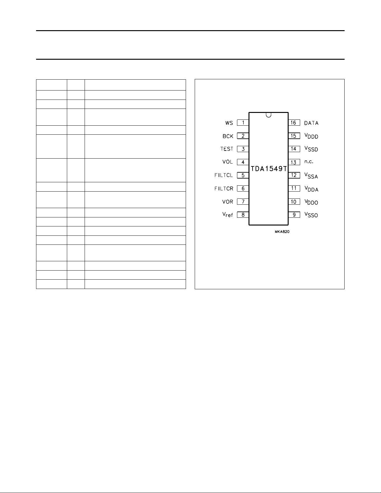
PINNING
SYMBOL PIN DESCRIPTION
WS 1 word select input
BCK 2 bit clock input
TEST 3 test input; pin should be connected to
ground
VOL 4 left channel output
FILTCL 5 capacitor for left channel 1st order
filter function; should be connected
between pins 4 and 5
FILTCR 6 capacitor for right channel 1st order
filter function; should be connected
between pins 6 and 7
VOR 7 right channel output
V
ref
V
SSO
V
DDO
V
DDA
V
SSA
n.c. 13 not connected (this pin should be left
V
SSD
V
DDD
DATA 16 data input
8 internal reference voltage for output
channels (1⁄2VDD)
9 operational amplifier ground
10 operational amplifier supply voltage
11 analog supply voltage
12 analog ground
open-circuit)
14 digital ground
15 digital supply voltage
TDA1549T
Fig.2 Pin configuration.
August 1994 5

Philips Semiconductors Objective specification
Stereo 4fs data input up-sampling filter with
bitstream continuous calibration DAC (BCC-DAC1)
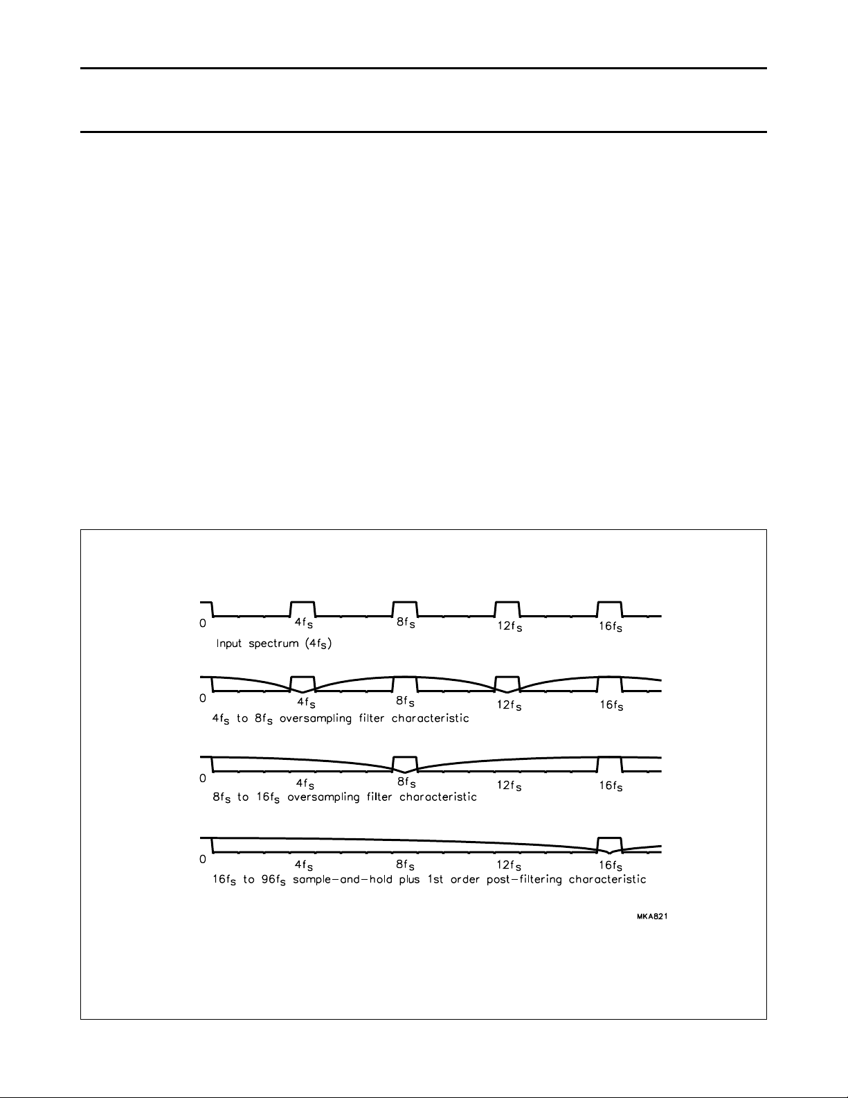
FUNCTIONAL DESCRIPTION
General
The TDA1549T CMOS digital-to-analog bitstream
continuous calibration converter incorporates internal
digital filtering which increases the oversampling rate of 4f
input data to 96fs, and removes the spectral data
components around 4fs, 8fs, and 12fs. A 2nd order noise
shaper operating at 96fs outputs a 5-bit data bitstream to
the DACs. The filtering required for waveform smoothing
and out-of-band noise reduction is achieved by simple 1st
order analog post-filtering (see Fig.3).
The combination of noise shaping and bitstream
continuous calibration digital-to-analog conversion
enables high performance and extremely low noise to be
achieved.
Input
The circuit accepts four times oversampled data in 18-bit
two's complement standard Japanese format with MSB
first. Left and right data channel words are time
multiplexed. The input format is illustrated in Fig.5. The bit
clock (BCK) operates at 192f
(WS) frequency of 4fs.
Oversampling filter
The oversampling filter consists of:
• A 7th order half-band low-pass FIR filter which
increases the oversampling rate from 4 times to 8 times.
This removes the spectral components around 4f
12fs (see Fig.3).
• A linear interpolation section which increases the
oversampling rate to 16 times. This removes the
spectral components around 8fs.
• A sample-and-hold section which provides another
6 times oversampling to 96 times.
, i.e. 48 times the word select
s
and
s
Noise Shaper
The 2nd-order digital noise shaper converts the 18-bit data
at 96f
into a 5-bit bitstream, while shifting in-band
s
quantization noise to frequencies well above the audio
band. For low signal levels the noise shaper output is a
s
1-bit bitstream. This noise shaping technique used in
combination with a special data code and bitstream DAC
enables extremely high signal-to-noise ratios to be
achieved.
Data encoder
The data encoder converts the 5-bit two's complement
output data from the noise shaper to a 32-bit thermometer
code.
In traditional unidirectional current converters, half of the
full-scale current flows to the output during small signal
reproduction. The thermal noise and substrate crosstalk
components present in this current severely restrict the
dynamic range which can be attained. In this BCC-DAC1
true low-noise performance is achieved using a special
data code and bidirectional current sources. The special
data code guarantees that only small values of current flow
to the output during small-signal passages while larger
positive or negative signals are generated using the
bidirectional current sources. For every change in the
18-bit input sample only one current source or current sink
is switched on. This intrinsically monotonic thermometer
code ensures the high differential linearity, zero crossover
distortion and superior signal-to-noise ratio associated
with bitstream conversion.
TDA1549T
The zero-order hold characteristic of this sample-and-hold
section plus the 1st order analog filtering removes the
spectral components around 16fs.
Passband ripple is within 0.1 dB. Stopband attenuation is
>50 dB around multiples of the sampling frequency.
August 1994 6
Philips Semiconductors Objective specification
Stereo 4fs data input up-sampling filter with
bitstream continuous calibration DAC (BCC-DAC1)
Continuous calibration DAC
The stereo 5-bit DAC uses the dynamic continuous
calibration technique. The DAC currents (16 sources and
16 sinks) of each channel are repeatedly generated from
one single reference current. This duplication is based on
an internal charge storage principle and has an inherently
high accuracy which is insensitive to ageing, temperature
and process variations.
Figure 4 shows one such current calibration source.
During calibration the cell is connected to the reference
current sink I
via switch S2. The calibration transistor M1
ref
is connected as an MOS diode via the switch S1 forcing its
gate potential to assume a value so that the total current of
the calibration cell is equal to the reference current. After
calibration the gate of M1 is allowed to float. The gate
capacitance Cgs retains its potential and the current
through the cell remains exactly equal to the reference
current. This current is now connected to the output. Each
digital-to-analog current source and each current sink is
calibrated precisely in this way.
Operational amplifiers
High precision, low-noise amplifiers together with the
internal conversion resistors R
the DAC output current to a voltage capable of driving a
line output. This voltage is available at VOL and VOR
(1.5 V RMS typical).
Connecting external capacitors C
FILTCL and VOL and FILTCR and VOR respectively,
provides the required 1st-order post-filtering for the left
and right channels (see Fig.1). The combinations of
R
CONV1
with C
1st order fall-off frequencies.
Internal reference circuitry
Internal reference circuitry ensures that the output voltage
signal is proportional to the supply voltage, thereby
maintaining maximum dynamic range for supply voltages
from 3.8 to 5.5 V and making the circuit also suitable for
battery-powered applications.
EXT1
and R
CONV2
CONV1
EXT1
with C
TDA1549T
and R
CONV2
and C
EXT2
between
EXT2
determine the
convert
Fig.3 Filter and noise shaper characteristics.
August 1994 7

Philips Semiconductors Objective specification
Stereo 4fs data input up-sampling filter with
bitstream continuous calibration DAC (BCC-DAC1)
TDA1549T
(a) calibration.
(b) operation.
Fig.4 Calibration principle.
August 1994 8
Philips Semiconductors Objective specification
Stereo 4fs data input up-sampling filter with
TDA1549T
bitstream continuous calibration DAC (BCC-DAC1)
LIMITING VALUES
In accordance with the Absolute Maximum Rating System (IEC 134).
SYMBOL PARAMETER CONDITIONS MIN. MAX. UNIT
V
DDD
V
DDA
V
DDO
T
xtal
T
stg
T
amb
V
es
Notes
1. Human body model: C = 100 pF; R = 1500 Ω.
2. Machine model: C = 200 pF; L = 0.5 µH; R = 10 Ω.
THERMAL CHARACTERISTICS
digital supply voltage − 7.0 V
analog supply voltage − 7.0 V
operational amplifier supply voltage − 7.0 V
maximum crystal temperature − +150 °C
storage temperature −65 +150 °C
operating ambient temperature −30 +85 °C
electrostatic handling note 1 −2000 +2000 V
note 2 −200 +200 V
SYMBOL PARAMETER VALUE UNIT
R
th j-a
thermal resistance from junction to ambient in free air 110 K/W
HANDLING
Inputs and outputs are protected against electrostatic discharge in normal handling. However, to be totally safe, it is
desirable to take normal precautions appropriate to handling MOS devices.
QUALITY SPECIFICATION
Quality specification in accordance with “
SNW-FQ-611
” is applicable.
August 1994 9

Philips Semiconductors Objective specification
Stereo 4fs data input up-sampling filter with
TDA1549T
bitstream continuous calibration DAC (BCC-DAC1)
CHARACTERISTICS
V
DDD=VDDA=VDDO
=5V; T
SYMBOL PARAMETER CONDITIONS MIN. TYP. MAX. UNIT
Supply
V
V
V
I
DDD
I
DDA
I
DDO
P
DDD
DDA
DDO
tot
digital supply voltage note 1 3.8 5.0 5.5 V
analog supply voltage note 1 3.8 5.0 5.5 V
operational amplifier supply voltage note 1 3.8 5.0 5.5 V
digital supply current note 2 − 12 18 mA
analog supply current note 2 − 5.5 8 mA
operational amplifier supply current note 2 − 6.5 9 mA
total power dissipation note 2 − 120 185 mW
RR ripple rejection note 4 − 25 − dB
Digital inputs; pins WS, BCK and DATA
V
IH
V
IL
| HIGH level input leakage current VIH=V
|I
LIH
| LOW level input leakage current VIH=V
|I
LIL
C
I
HIGH level input voltage 0.7VDD− VDD + 0.5 V
LOW level input voltage −0.5 − 0.3V
input capacitance −− 10 pF
Timing (see Fig.6)
=25°C; unless otherwise specified.
amb
note 3 − 50 − mW
=5V −− 10 µA
DDD
=0V −− 10 µA
SSD
DD
V
PERATING FREQUENCY
O
f
BCK
f
WS
bit clock frequency − 192f
word select frequency − f
BCK
s
− Hz
/48 − Hz
INPUT FREQUENCY
f
BCK
clock frequency −− 9.216 MHz
BR bit rate data input −− 9.216 MHz
f
WS
t
r
t
f
T
cy
t
H
t
L
t
su
t
h
t
hWS
t
suWS
word select input frequency −− 192 kHz
rise time −− 32 ns
fall time −− 32 ns
bit clock cycle time 108 −−ns
bit clock HIGH time 22 −−ns
bit clock LOW time 22 −−ns
data set-up time 32 −−ns
data hold time 2 −−ns
word select hold time 2 −−ns
word select set-up time 32 −−ns
Filter characteristics (see Fig.3)
PBR pass-band ripple < 20 kHz − 0.1 − dB
SBA stop-band attenuation note 5 50 −−dB
August 1994 10

Philips Semiconductors Objective specification
Stereo 4fs data input up-sampling filter with
TDA1549T
bitstream continuous calibration DAC (BCC-DAC1)
SYMBOL PARAMETER CONDITIONS MIN. TYP. MAX. UNIT
Reference values
V
ref
R
CONV
Analog outputs; pins VOL and VOR
RES resolution −− 18 bit
V
FS(rms)
V
OFF
TC
FS
(THD + N)/S total harmonic distortion plus
S/N signal-to-noise ratio at bipolar zero A-weighted;
t
cs
α
cs
| unbalance between outputs − 0.2 0.3 dB
|∆V
O
| dynamic output impedance − 10 − W
|Z
O
R
L
C
L
Notes
1. All VDD and VSS pins must be connected externally to the same supply.
2. Measured with V
3. Measured with V
4. V
ripple
external capacitor (C
5. Around multiples of 4fs.
6. Measured with a 1 kHz, 0 dB, 18-bit sine wave generated at a sampling rate of 192 kHz.
(THD + N)/S measured over a bandwidth from 20 Hz to 20 kHz.
7. Measured with a 1 kHz, −60 dB, 18-bit sine wave generated at a sampling rate of 192 kHz. (THD + N)/S measured
over a bandwidth from 20 Hz to 20 kHz.
8. Measured with a 1 kHz, −60 dB, 18-bit sine wave generated at a sampling rate of 192 kHz.
(THD + N)/S measured over a bandwidth from 20 Hz to 20 kHz and filtered with A-weighted characteristic.
9. Measured with a 0 dB, 18-bit sine wave from 20 Hz to 20 kHz generated at a sampling rate of 192 kHz. (THD + N)/S
measured over a bandwidth from 20 Hz to 20 kHz.
reference voltage level 2.45 2.5 2.55 V
current-to-voltage conversion
1.6 2.2 2.8 kΩ
resistance
full-scale output voltage (RMS value) 1.425 1.5 1.575 V
output voltage DC offset with respect
to reference voltage level V
ref
−80 −65 −50 mV
full-scale temperature coefficient −±100x10−6−
noise-to-signal ratio
at 0 dB input level;
note 6
at −60 dB input level;
note 7
at −60 dB input level;
A-weighted; note 8
at 0 dB input level;
20 Hz to 20 kHz;
−−90 −83 dB
− 0.003 0.007 %
−−48 −40 dB
− 0.40 1.0 %
−−50 − dB
− 0.32 − %
−−90 −83 dB
− 0.003 0.007 %
note 9
100 110 − dB
at code 00000H
current setting time to ±1 LSB − 0.1 − ms
channel separation 85 100 − dB
output load resistance 3 −−kΩ
output load capacitance −− 200 pF
DDD=VDDA=VDDO
DDD=VDDA=VDDO
= 1% of the supply voltage and f
in Fig.1) connected to V
EXT3
= 5 V at input data code 00000H.
= 3.8 V at input data code 00000H.
= 100 Hz. Ripple rejection RR to V
ripple
. The value quoted here assumes C
ref
is dependent on the value of the
DDA
=1µF.
EXT3
August 1994 11

Philips Semiconductors Objective specification
Stereo 4fs data input up-sampling filter with
bitstream continuous calibration DAC (BCC-DAC1)
TDA1549T
Fig.5 Format of input signals.
August 1994 12
Fig.6 Timing of input signals.

Philips Semiconductors Objective specification
Stereo 4fs data input up-sampling filter with
TDA1549T
bitstream continuous calibration DAC (BCC-DAC1)
APPLICATION INFORMATION
A typical application diagram is illustrated in Fig.7. The left and right channel outputs can drive a line output directly.
(1) C = 100 nF (chip capacitor).
Fig.7 Application diagram.
August 1994 13

Philips Semiconductors Objective specification
Stereo 4fs data input up-sampling filter with
bitstream continuous calibration DAC (BCC-DAC1)
TDA1549T
(1) Level = −60 dB.
(2) Level = 0 dB.
Fig.8 Total harmonic distortion plus noise-to-signal ratio as a function of signal frequency.
In Fig.8 measurements were taken with an 18-bit sine wave generated at a sample rate of 192 kHz. The (THD + N)/S
was measured over a bandwidth of 20 Hz to 20 kHz.
The graph was constructed from average measurement values of a small amount of engineering samples. No guarantee
for typical values is implied.
August 1994 14
Philips Semiconductors Objective specification
Stereo 4fs data input up-sampling filter with
bitstream continuous calibration DAC (BCC-DAC1)
TDA1549T
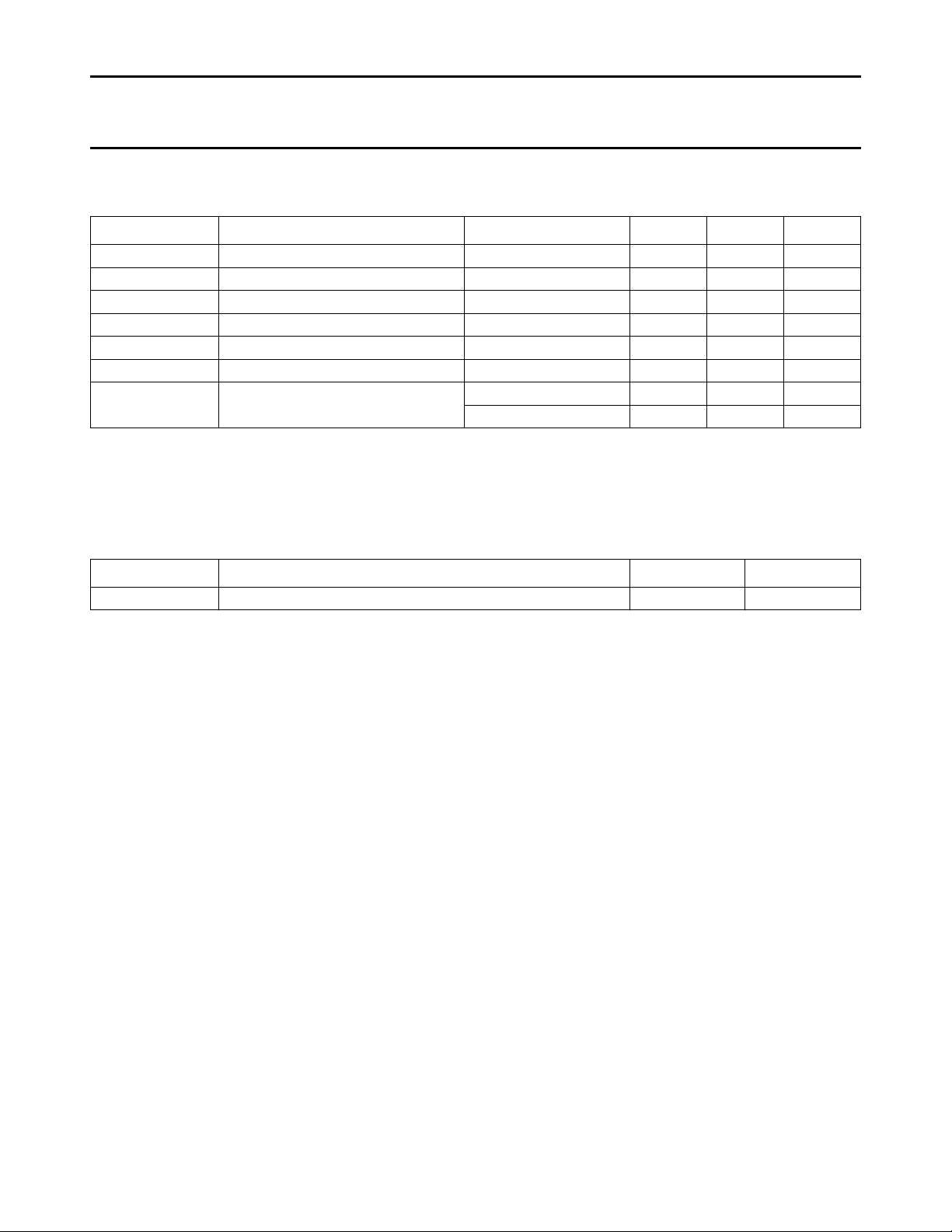
Fig.9 Total harmonic distortion plus noise-to-signal ratio as a function of signal level; (A-weighted).
In Fig.9 measurements were taken with an 18-bit sine wave generated at a sample rate of 192 kHz. The (THD + N)/S
was measured over a bandwidth of 20 Hz to 20 kHz and filtered with A-weighted characteristic.
The graph was constructed from average measurement values of a small amount of engineering samples. No guarantee
for typical values is implied.
August 1994 15
Philips Semiconductors Objective specification
Stereo 4fs data input up-sampling filter with
bitstream continuous calibration DAC (BCC-DAC1)
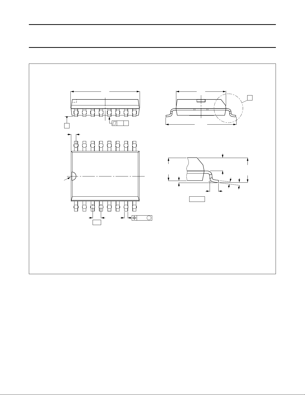
PACKAGE OUTLINE
(4x)
10.5
10.1
0.1 S
9
2.45
0.3
2.25
0.1
handbook, full pagewidth
S
0.9
0.4
16
pin 1
index
18
7.6
7.4
10.65
10.00
detail A
1.1
0.5
1.1
1.0
TDA1549T
A
0 to 8
MBC233 - 1
2.65
2.35
o
0.32
0.23
Dimensions in mm.
1.27
0.49
0.36
0.25 M
(16x)
Fig.10 Plastic small outline package; 16 leads; body width 7.5 mm; (SO16; SOT162-1).
August 1994 16

Philips Semiconductors Objective specification
Stereo 4fs data input up-sampling filter with
bitstream continuous calibration DAC (BCC-DAC1)
SOLDERING
Plastic small-outline packages
YWAVE
B
During placement and before soldering, the component
must be fixed with a droplet of adhesive. After curing the
adhesive, the component can be soldered. The adhesive
can be applied by screen printing, pin transfer or syringe
dispensing.
Maximum permissible solder temperature is 260 °C, and
maximum duration of package immersion in solder bath is
10 s, if allowed to cool to less than 150 °C within 6 s.
Typical dwell time is 4 s at 250 °C.
A modified wave soldering technique is recommended
using two solder waves (dual-wave), in which a turbulent
wave with high upward pressure is followed by a smooth
laminar wave. Using a mildly-activated flux eliminates the
need for removal of corrosive residues in most
applications.
Y SOLDER PASTE REFLOW
B
Several techniques exist for reflowing; for example,
thermal conduction by heated belt, infrared, and
vapour-phase reflow. Dwell times vary between 50 and
300 s according to method. Typical reflow temperatures
range from 215 to 250 °C.
Preheating is necessary to dry the paste and evaporate
the binding agent. Preheating duration: 45 min at 45 °C.
EPAIRING SOLDERED JOINTS (BY HAND-HELD SOLDERING
R
IRON OR PULSE
Fix the component by first soldering two, diagonally
opposite, end pins. Apply the heating tool to the flat part of
the pin only. Contact time must be limited to 10 s at up to
300 °C. When using proper tools, all other pins can be
soldered in one operation within 2 to 5 s at between 270
and 320 °C. (Pulse-heated soldering is not recommended
for SO packages.)
For pulse-heated solder tool (resistance) soldering of VSO
packages, solder is applied to the substrate by dipping or
by an extra thick tin/lead plating before package
placement.
TDA1549T
-HEATED SOLDER TOOL)
Reflow soldering requires the solder paste (a suspension
of fine solder particles, flux and binding agent) to be
applied to the substrate by screen printing, stencilling or
pressure-syringe dispensing before device placement.
DEFINITIONS
Data sheet status
Objective specification This data sheet contains target or goal specifications for product development.
Preliminary specification This data sheet contains preliminary data; supplementary data may be published later.
Product specification This data sheet contains final product specifications.
Limiting values
Limiting values given are in accordance with the Absolute Maximum Rating System (IEC 134). Stress above one or
more of the limiting values may cause permanent damage to the device. These are stress ratings only and operation
of the device at these or at any other conditions above those given in the Characteristics sections of the specification
is not implied. Exposure to limiting values for extended periods may affect device reliability.
Application information
Where application information is given, it is advisory and does not form part of the specification.
LIFE SUPPORT APPLICATIONS
These products are not designed for use in life support appliances, devices, or systems where malfunction of these
products can reasonably be expected to result in personal injury. Philips customers using or selling these products for
use in such applications do so at their own risk and agree to fully indemnify Philips for any damages resulting from such
improper use or sale.
August 1994 17

Philips Semiconductors Objective specification
Stereo 4fs data input up-sampling filter with
bitstream continuous calibration DAC (BCC-DAC1)
NOTES
TDA1549T
August 1994 18

Philips Semiconductors Objective specification
Stereo 4fs data input up-sampling filter with
TDA1549T
bitstream continuous calibration DAC
NOTES
August 1994 19

Philips Semiconductors – a worldwide company
Argentina: IEROD, Av. Juramento 1992 - 14.b, (1428)
BUENOS AIRES, Tel. (541)786 7633, Fax. (541)786 9367
Australia: 34 Waterloo Road, NORTH RYDE, NSW 2113,
Tel. (02)805 4455, Fax. (02)805 4466
Austria: Triester Str. 64, A-1101 WIEN, P.O. Box 213,
Tel. (01)60 101-1236, Fax. (01)60 101-1211
Belgium: Postbus 90050, 5600 PB EINDHOVEN, The Netherlands,
Tel. (31)40 783 749, Fax. (31)40 788 399
Brazil: Rua do Rocio 220 - 5
CEP: 04552-903-SÃO PAULO-SP, Brazil.
P.O. Box 7383 (01064-970).
Tel. (011)821-2333, Fax. (011)829-1849
Canada: PHILIPS SEMICONDUCTORS/COMPONENTS:
Tel. (800) 234-7381, Fax. (708) 296-8556
Chile: Av. Santa Maria 0760, SANTIAGO,
Tel. (02)773 816, Fax. (02)777 6730
Colombia: IPRELENSO LTDA, Carrera 21 No. 56-17,
77621 BOGOTA, Tel. (571)249 7624/(571)217 4609,
Fax. (571)217 4549
Denmark: Prags Boulevard 80, PB 1919, DK-2300 COPENHAGEN S,
Tel. (032)88 2636, Fax. (031)57 1949
Finland: Sinikalliontie 3, FIN-02630 ESPOO,
Tel. (9)0-50261, Fax. (9)0-520971
France: 4 Rue du Port-aux-Vins, BP317,
92156 SURESNES Cedex,
Tel. (01)4099 6161, Fax. (01)4099 6427
Germany: P.O. Box 10 63 23, 20043 HAMBURG,
Tel. (040)3296-0, Fax. (040)3296 213.
Greece: No. 15, 25th March Street, GR 17778 TAVROS,
Tel. (01)4894 339/4894 911, Fax. (01)4814 240
Hong Kong: PHILIPS HONG KONG Ltd., 6/F Philips Ind. Bldg.,
24-28 Kung Yip St., KWAI CHUNG, N.T.,
Tel. (852)424 5121, Fax. (852)428 6729
India: Philips INDIA Ltd, Shivsagar Estate, A Block ,
Dr. Annie Besant Rd. Worli, Bombay 400 018
Tel. (022)4938 541, Fax. (022)4938 722
Indonesia: Philips House, Jalan H.R. Rasuna Said Kav. 3-4,
P.O. Box 4252, JAKARTA 12950,
Tel. (021)5201 122, Fax. (021)5205 189
Ireland: Newstead, Clonskeagh, DUBLIN 14,
Tel. (01)640 000, Fax. (01)640 200
Italy: PHILIPS SEMICONDUCTORS S.r.l.,
Piazza IV Novembre 3, 20124 MILANO,
Tel. (0039)2 6752 2531, Fax. (0039)2 6752 2557
Japan: Philips Bldg13-37, Kohnan 2-chome, Minato-ku, TOKYO 108,
Tel. (03)3740 5028, Fax. (03)3740 0580
Korea: (Republic of) Philips House, 260-199 Itaewon-dong,
Yongsan-ku, SEOUL, Tel. (02)794-5011, Fax. (02)798-8022
Malaysia: No. 76 Jalan Universiti, 46200 PETALING JAYA,
SELANGOR, Tel. (03)750 5214, Fax. (03)757 4880
Mexico: 5900 Gateway East, Suite 200, EL PASO, TX 79905,
Tel. 9-5(800)234-7381, Fax. (708)296-8556
Netherlands: Postbus 90050, 5600 PB EINDHOVEN, Bldg. VB
Tel. (040)783749, Fax. (040)788399
New Zealand: 2 Wagener Place, C.P.O. Box 1041, AUCKLAND,
Tel. (09)849-4160, Fax. (09)849-7811
Norway: Box 1, Manglerud 0612, OSLO,
Tel. (022)74 8000, Fax. (022)74 8341
th
floor, Suite 51,
Pakistan: Philips Electrical Industries of Pakistan Ltd.,
Exchange Bldg. ST-2/A, Block 9, KDA Scheme 5, Clifton,
KARACHI 75600, Tel. (021)587 4641-49,
Fax. (021)577035/5874546.
Philippines: PHILIPS SEMICONDUCTORS PHILIPPINES Inc,
106 Valero St. Salcedo Village, P.O. Box 2108 MCC, MAKATI,
Metro MANILA, Tel. (02)810 0161, Fax. (02)817 3474
Portugal: PHILIPS PORTUGUESA, S.A.,
Rua dr. António Loureiro Borges 5, Arquiparque - Miraflores,
Apartado 300, 2795 LINDA-A-VELHA,
Tel. (01)14163160/4163333, Fax. (01)14163174/4163366.
Singapore: Lorong 1, Toa Payoh, SINGAPORE 1231,
Tel. (65)350 2000, Fax. (65)251 6500
South Africa: S.A. PHILIPS Pty Ltd.,
195-215 Main Road Martindale, 2092 JOHANNESBURG,
P.O. Box 7430 Johannesburg 2000,
Tel. (011)470-5911, Fax. (011)470-5494.
Spain: Balmes 22, 08007 BARCELONA,
Tel. (03)301 6312, Fax. (03)301 42 43
Sweden: Kottbygatan 7, Akalla. S-164 85 STOCKHOLM,
Tel. (0)8-632 2000, Fax. (0)8-632 2745
Switzerland: Allmendstrasse 140, CH-8027 ZÜRICH,
Tel. (01)488 2211, Fax. (01)481 77 30
Taiwan: PHILIPS TAIWAN Ltd., 23-30F, 66, Chung Hsiao West
Road, Sec. 1. Taipeh, Taiwan ROC, P.O. Box 22978,
TAIPEI 100, Tel. (02)388 7666, Fax. (02)382 4382.
Thailand: PHILIPS ELECTRONICS (THAILAND) Ltd.,
209/2 Sanpavuth-Bangna Road Prakanong,
Bangkok 10260, THAILAND,
Tel. (662)398-0141, Fax. (662)398-3319.
Turkey:Talatpasa Cad. No. 5, 80640 GÜLTEPE/ISTANBUL,
Tel. (0212)279 2770, Fax. (0212)269 3094
United Kingdom: Philips Semiconductors LTD.,
276 Bath road, Hayes, MIDDLESEX UB3 5BX,
Tel. (081)73050000, Fax. (081)7548421
United States:811 East Arques Avenue, SUNNYVALE,
CA 94088-3409, Tel. (800)234-7381, Fax. (708)296-8556
Uruguay: Coronel Mora 433, MONTEVIDEO,
Tel. (02)70-4044, Fax. (02)92 0601
For all other countries apply to: Philips Semiconductors,
International Marketing and Sales, Building BE-p,
P.O. Box 218, 5600 MD, EINDHOVEN, The Netherlands,
Telex 35000 phtcnl, Fax. +31-40-724825
SCD34 © Philips Electronics N.V. 1994
All rights are reserved. Reproduction in whole or in part is prohibited without the
prior written consent of the copyright owner.
The information presented in this document does not form part of any quotation
or contract, is believed to be accurate and reliable and may be changed without
notice. No liability will be accepted by the publisher for any consequence of its
use. Publication thereof does not convey nor imply any license under patent- or
other industrial or intellectual property rights.
Printed in The Netherlands
Philips Semiconductors

WWW.ALLDATASHEET.COM
Copyright © Each Manufacturing Company.
All Datasheets cannot be modified without permission.
This datasheet has been download from :
www.AllDataSheet.com
100% Free DataSheet Search Site.
Free Download.
No Register.
Fast Search System.
www.AllDataSheet.com
 Loading...