

Philips TDA1516CQ Datasheet

INTEGRATED CIRCUITS
DATA SH EET
TDA1516CQ
24 W BTL car radio power amplifier
Product specification
File under Integrated Circuits, IC01
July 1994

Philips Semiconductors Product specification
24 W BTL car radio power amplifier TDA1516CQ
FEATURES
• Requires very few external components for Bridge-TiedLoad (BTL)
• High output power (without bootstrap)
• Low offset voltage at output (important for BTL)
• Fixed gain
• Capability to handle high energy on outputs (V
• Protected against electrostatic discharge
• No switch-on/switch-off plop
• Flexible leads
• Low thermal resistance
• Identical inputs (inverting and non-inverting).
= 0)
P
• Good ripple rejection
• Mute/stand-by switch
• Load dump protection
• AC and DC short-circuit-safe to ground and V
• Thermally protected
P
GENERAL DESCRIPTION
The TDA1516CQ is a monolithic integrated class-B output
amplifier in a 13-lead single-in-line (SIL) plastic power
package. The device is primarily developed for car radio
applications.
• Reverse polarity safe
QUICK REFERENCE DATA
SYMBOL PARAMETER CONDITIONS MIN. TYP. MAX. UNIT
V
P
positive supply voltage range
operating 6.0 14.4 18 V
non-operating −−30 V
load dump −−45 V
I
ORM
I
P
I
sb
I
sw
Z
input impedance BTL 25 −−kΩ
I
T
XTAL
P
O
SVRR supply voltage ripple rejection R
repetitive peak output current −−4A
total quiescent current − 40 80 mA
stand-by current − 0.1 100 µA
switch-on current −−60 µA
crystal temperature −−+150 °C
output power THD = 10%; 4 Ω−22 − W
= 0; f = 100 Hz 45 −−dB
S
f = 1 to 10 kHz 48 −−dB
V
no
∆V
os
noise output voltage − 70 −µV
DC output offset voltage −−100 mV
ORDERING INFORMATION
EXTENDED TYPE
NUMBER
PINS PIN POSITION MATERIAL CODE
TDA1516CQ 13 DIL plastic SOT141
Note
1. SOT141-6; 1996 August 21.
July 1994 2
PACKAGE
(1)
Philips Semiconductors Product specification
24 W BTL car radio power amplifier TDA1516CQ
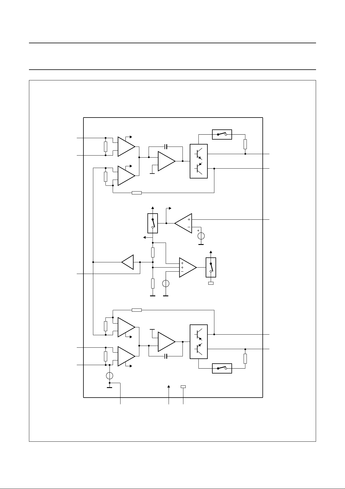
handbook, full pagewidth
bootstrap switch
2
60
kΩ
1
2
kΩ
12
mute switch
VA
kΩ
18
stand-by
switch
VA
x1
kΩ
15
kΩ
15
C
m
power stage
V
P
bootstrap switch
mute
reference
voltage
stand-by
reference
voltage
mute
switch
100
Ω
5
6
11
TDA1516CQ
18 kΩ
2
kΩ
13
60
kΩ
4
input
reference
voltage
VA
signal
ground
mute switch
C
m
V
Fig.1 Block diagram.
July 1994 3
power stage
9
8
100
Ω
P
power
ground
(substrate)
7103
bootstrap switch
MBC084
 Loading...