


INTEGRATED CIRCUITS
DATA SH EET
TDA1300T
Photodetector amplifiers and laser
supply
Product specification
Supersedes data of 1995 Sep 27
File under Integrated Circuits, IC01
1995 Nov 16

Philips Semiconductors Product specification
Photodetector amplifiers and laser
supply
FEATURES
• Six input buffer amplifiers with low-pass filtering with
virtually no offset
• HF data amplifier with a high or low gain mode
• Two built-in equalizers for single or double speed mode
ensuring high playability in both modes
• Full automatic laser control including stabilization and
an on/off switch and containing a separate supply V
for power reduction
• Applicable with N-sub laser with N-sub or P-sub monitor
diode
• Adjustable laser bandwidth and laser switch-on current
slope
• Protection circuit preventing laser damage due to supply
voltage dip
• Optimized interconnect between pick-up detector and
TDA1301
• Wide supply voltage range
• Wide temperature range
• Low-power consumption.
DDL
TDA1300T
GENERAL DESCRIPTION
The TDA1300 is an integrated data amplifier and laser
supply for three beam pick-up detectors applied in a wide
range of mechanisms for Compact Disc and Read Only
optical systems. It offers 6 amplifiers which amplify and
filter the focus and radial diode signals adequately and
provides an equalized RF signal for single or double speed
mode which can be switched by means of the speed
control pin.
The device can handle astigmatic, single foucault and
double foucault detectors and is applicable with all N-sub
laser, N-sub or P-sub monitor diode units.
After a single initial adjustment the circuit keeps control
over the laser diode current resulting in a constant light
output power independent of ageing. The chip is mounted
in a small SO24 package enabling mounting close to the
laser pick-up unit on the sledge.
QUICK REFERENCE DATA
SYMBOL PARAMETER CONDITIONS MIN. TYP. MAX. UNIT
V
DD
supply voltage 3 − 5.5 V
Diode current amplifiers 6 times
G
dn
I
os(d)
B 3 dB bandwidth I
amplification 1.43 1.55 1.67
offset current −−100 nA
= 1.67 µA50−−kHz
i(d)
RFE amplifier (built-in equalizer)
t
d(eq)
t
d(f)
equalization delay time fi= 0.3 MHz − 320 − ns
flatness delay time double-speed − 5 − ns
Laser supply
I
o(l)
output current V
=3V −−−100 mA
DDL
ORDERING INFORMATION
PACKAGE
TYPE NUMBER
NAME DESCRIPTION VERSION
TDA1300T SO24 plastic small outline package; 24 leads; body width 7.5 mm SOT137-1
1995 Nov 16 2
Philips Semiconductors Product specification
Photodetector amplifiers and laser supply TDA1300T
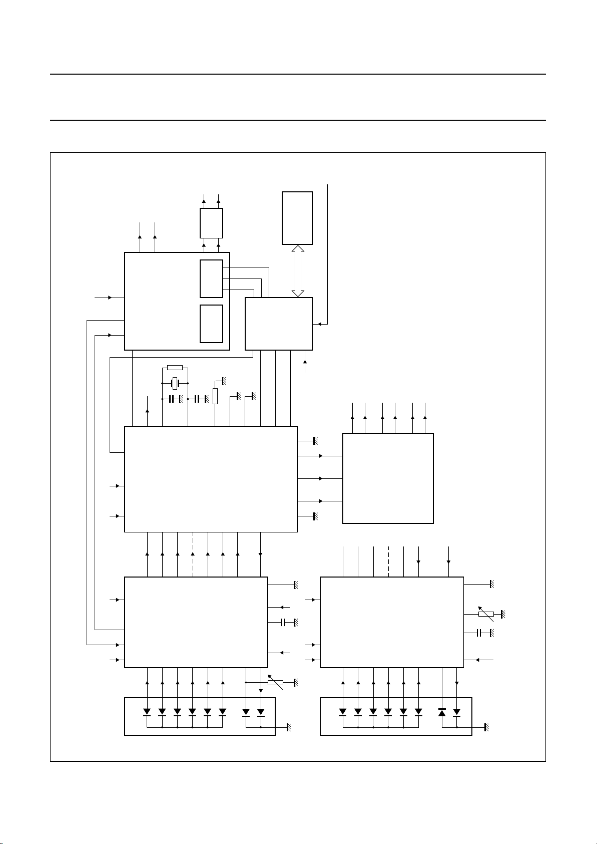
SCHEMATIC DIAGRAM
to
motor
spindle
left
right
clk
(SAA7345)
DECODER
PLL
AMP
POWER
SUBCODE
DECODER
MOTOR
CONTROL
KEYBORD
DISPLAY
PROCESSOR
DISPLAY
end_stop_switch
MBG473
DDD
V
DDA
V
NRST
DDD
V
DDA
V
DD
V
G SP RF(E)
OTD
CLO
D1
O1
I1
XTLI
D2
O2
DIODE
I2
XTLO
DIGITAL SERVO IC
D3
D4
O3
O4
AND
LASER
AMPLIFIER
I3
I4
XTLR
R1
O5
SUPPLY
I5
TS1
TDA1301
R2
V
O6
TDA1300
I6
RL
TS2
V
MI
RH
SICL
LDON
LDON
LO
SIDA
O ADJ GND
DDL
V
SILD
1 nF
clk
SSD
RA FO SL V
SSK
V
DD
V
2.5 to 5 V
DD
V
G SP RF(E)
O1
I1
focus
O2
I2
actuator
DIODE
O3
AMPLIFIER
I3
radial
actuator
sledge
(TDA7072/7073)
POWER AMPLIFIER
O4
O5
O6
AND
LASER
SUPPLY
TDA1300
I4
I5
I6
MI
LDON
LO
O ADJ GND
DDL
V
1 nF
ADJp
R
2.5 to 5 V
handbook, full pagewidth
Fig.1 Schematic diagram for CD player.
photo-
configuration
N-sub monitor
1995 Nov 16 3
diodes
mon
ADJn
R
la
photo-
diodes
configuration
P-sub monitor
mon
la
Philips Semiconductors Product specification
Photodetector amplifiers and laser supply TDA1300T
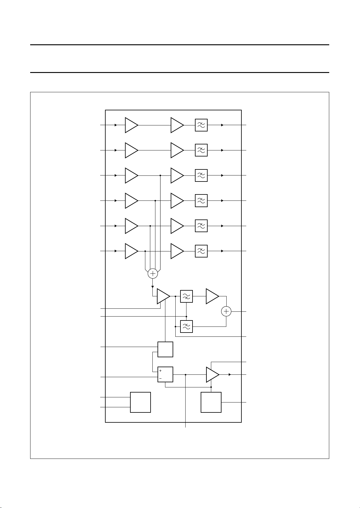
BLOCK DIAGRAM
handbook, full pagewidth
I6
23 2
in
I6
6
1.5x
Id6
out
O6
HG
LS
I5
20
in
I5
24
I4
22
I3
19
I2
21
I1
11
12
5
I4
in
4
I3
in
3
I2
in
2
I1
in
1
I
csin
1.5x
1.5x
1.5x
1.5x
1.5x
95, 120, 134 or
240 kΩ
I/V
−4
Id5
Id4
Id3
Id2
Id1
TDA1300T
out
out
out
out
out
5
O5
1
O4
3
O3
6
O2
4
O1
9
RFE
1995 Nov 16 4
ADJ
V
DD
GND
10
14
I
(P-sub)
ADJ
(N-sub) or
V
mon
17
MI
I
(P-sub)
mon
18
15
SUPPLY
V
gap
OTA
CL
ILO
ON/OFF
13
MBG474
(N-sub) or
V
DD
RF
8
V
DDL
16
LO
7
LDON
Fig.2 Block diagram.
Philips Semiconductors Product specification
Photodetector amplifiers and laser supply TDA1300T
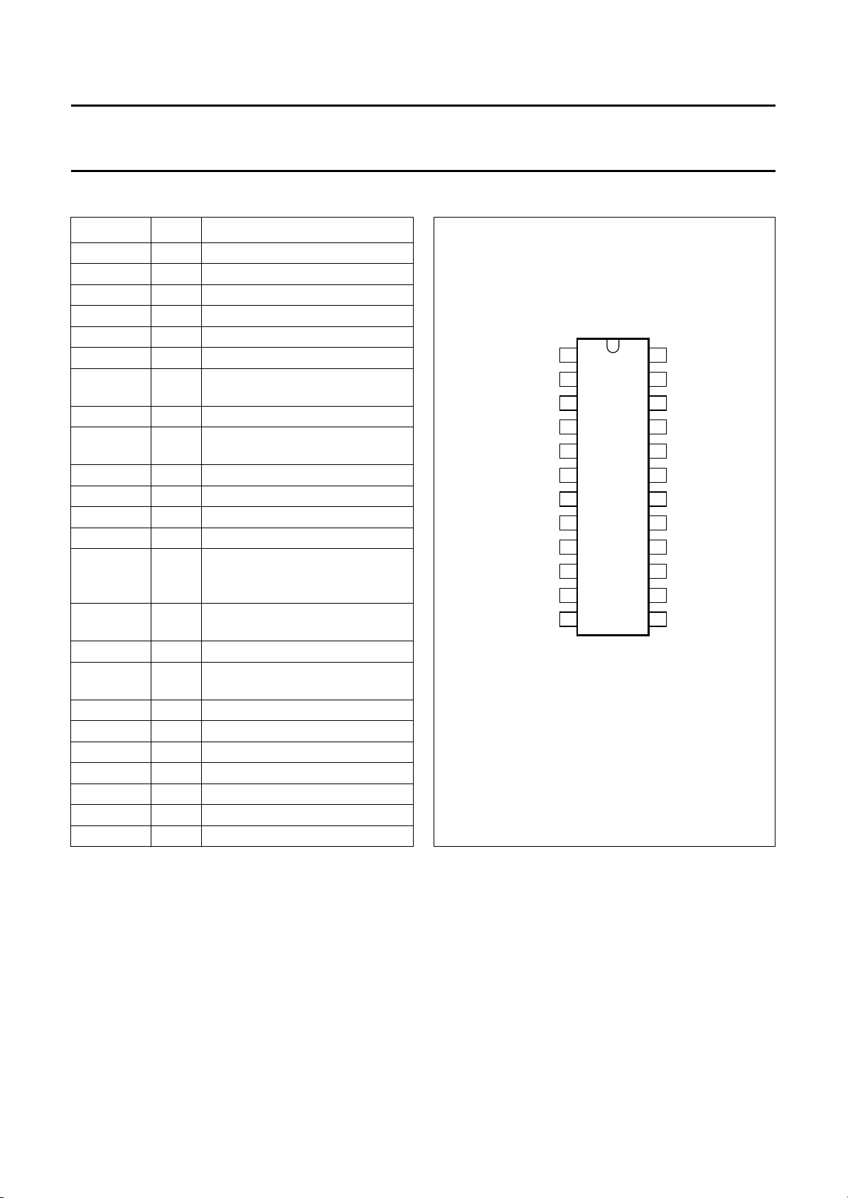
PINNING
SYMBOL PIN DESCRIPTION
O4 1 output of current amplifier 4
O6 2 output of current amplifier 6
O3 3 output of current amplifier 3
O1 4 output of current amplifier 1
O5 5 output of current amplifier 5
O2 6 output of current amplifier 2
LDON 7 control pin for switching the laser
on and off
V
DDL
8 laser supply voltage
RFE 9 equalized output voltage of sum
signal of amplifiers 1 to 4
RF 10 unequalized output
HG 11 control pin for gain switch
LS 12 control pin for speed switch
CL 13 external capacitor
ADJ 14 if connected via resistor to GND
P-sub monitor. If connected to
N-sub monitor
V
DD
GND 15 zero supply connection,
substrate connection
LO 16 output for the laser, current output
MI 17 input for the monitor diode of the
laser
V
DD
18 positive supply connection
I2 19 photo detector input 2 (central)
I5 20 photo detector input 5 (satellite)
I1 21 photo detector input 1 (central)
I3 22 photo detector input 3 (central)
I6 23 photo detector input 6 (satellite)
I4 24 photo detector input 4 (central)
handbook, halfpage
1
O4
2
O6
3
O3
4
O1
5
O5
6
O2
TDA1300T
7
LDON
8
V
DDL
9
RFE
10
RF
11
HG
12
LS
MBG472
Fig.3 Pin configuration.
24
I4
23
I6
22
I3
21
I1
20
I5
19
I2
18
V
DD
17
MI
16
LO
15
GND
14
ADJ
13
CL
1995 Nov 16 5

Philips Semiconductors Product specification
Photodetector amplifiers and laser supply TDA1300T
FUNCTIONAL DESCRIPTION
The TDA1302T can be divided into two main sections:
1. Laser control circuit
2. Photo diode signal filter and amplification section.
Laser control circuit
The main function of the laser control circuit is to control
the laser diode current in order to achieve a constant light
output power. This is done by monitoring the monitor
diode. There is a fixed relation between light output power
of the laser and the current of the monitor diode. The circuit
can handle P-sub or N-sub monitor diodes.
MONITOR
N-sub
In this event pin 14 (ADJ) must be connected to the
positive supply voltage VDD to select the N-sub mode. With
an adjustable resistor (R
) across the diode the monitor
ADJn
current can be adjusted (and so the laser light output
power) if one knows that the control circuit keeps the
monitor voltage V
at a constant level of
mon
approximately 150 mV.
MONITOR
P-sub
R
ADJn
---------------C
L
KA
× 8709–×10×≅
ext
(Hz) in case of
f
BN
N-sub monitor
where A
amplifier, if applied, and K = ∆I
determined by the laser/monitor unit. I
represents the AC gain of an extra loop
ext
/∆I
laser
mon
which is
is the
mon
average current (pin 17) at typical light emission power
of the laser diode.
The third part is the power output stage, its input being the
integrator output signal. This stage has a separate supply
voltage (V
) thereby offering the possibility of reduced
DDL
power consumption by supplying this pin with the minimum
voltage necessary.
It also has a laser diode protection circuit which comes into
action just before the driving output transistor will get
saturated due to a large voltage dip on V
. Saturation
DDL
will result in a lower current of the laser diode, which
normally is followed immediately by an increment of the
voltage of the external capacitor CL. This could cause
damage to the laser diode at the end of the dip. The
protection circuit prevents an increment of the capacitor
voltage and thus offers full protection to the laser diode
under these circumstances.
In this event pin 14 (ADJ) is connected via resistor R
ADJp
to ground. The P-sub mode is selected and pin 14 (ADJ)
acts as reference bandgap voltage, providing together with
R
an adjustable current l
ADJp
keeps the monitor current at a level which is 10 × l
. Now the control circuit
ADJ
ADJ
.
The circuit is built-up in three parts:
The first part is the input stage which is able to switch
between both modes (N-sub or P-sub).
The second part is the integrator part which makes use of
an external capacitor CL. This capacitor has two different
functions:
1. During switch-on of the laser current, it provides a
current slope of typically:
≅
10
----------C
6–
(A/s)
L
∆I
LO
----------- t∆
2. After switch-on it ensures that the bandwidth is in
accordance with the typical formula:
KA
× 909–×10×
f
≅
BP
ext
-------------------------------------------------
×
C
LImon
(Hz) in case of
P-sub monitor.
Photo diode signal filter and amplification section
This section has 6 identical current amplifiers.
Amplifiers 1 to 4 are designed to amplify the focus photo
diode signals. Each amplifier has two outputs, an
LF output and an internal RF output. Amplifiers 5 and 6
are used for the radial photo diode currents and only have
a LF output. All 6 output signals are low-pass filtered with
a corner frequency at 69 kHz. The internal RF output
signals are summed together and converted to a voltage
afterwards by means of a selectable transresistance.
This transresistance R
can be changed between 140 kΩ
RF
(3.3 V application) or 240 kΩ (5 V application) in
combination with the P-sub monitor. In the event of the
N-sub monitor selection, RRF can be changed between
70 kΩ (3.3 V application) and 120 kΩ (5 V application).
The RF signal is available directly at pin 10 but there is
also an unfiltered signal available at pin 9.
The used equalization filter has 2 different filter curves:
1. One for single-speed mode
2. One for double-speed mode.
1995 Nov 16 6

Philips Semiconductors Product specification
Photodetector amplifiers and laser supply TDA1300T
Table 1 Gain and monitor modes
PIN MODE
HG ADJ R
0R
to ground 140 kΩ P-sub
ADJp
0 1 70 kΩ N-sub
(1)
1
(1)
1
R
to ground 240 kΩ P-sub
ADJp
1 120 kΩ N-sub
Note
1. Logic 1 or not connected.
Table 2 Speed and laser modes; note 1
PIN DEFAULT
LS
LDON
(2)
11 0X
1X
Notes
1. 1 = HIGH voltage V
; 0 = LOW voltage GND; X = don’t care.
DD
2. If not connected.
3. X = don’t care.
RF
MONITOR
3.3 V
5V
MODE
SPEED LASER
SINGLE DOUBLE on off
INTENDED APPLICATION AREA
(3)
(3)
(3)
X
10
X
(3)
LIMITING VALUES
In accordance with the Absolute Maximum Rating System (IEC 134).
SYMBOL PARAMETER CONDITIONS MIN. MAX. UNIT
V
DD
P
max
T
stg
T
amb
(1)
V
es
supply voltage − 8V
maximum power dissipation − 300 mW
storage temperature −65 +150 °C
operating ambient temperature −40 +85 °C
electrostatic handling pin 16 note 2 −2+2kV
electrostatic handling (all other pins) −3+3kV
Notes
1. Classification A: human body model; C = 100 pF; R = 1500 Ω; V = ± 2000 V.
Charge device model: C = 200 pF; L = 2.5 µH; R = 0 Ω; V = 250 V.
2. Equivalent to discharging a 100 pF capacitor through a 1.5 kΩ series resistor.
THERMAL RESISTANCE
SYMBOL PARAMETER VALUE UNIT
R
th j-a
from junction to ambient in free air 60 K/W
1995 Nov 16 7

Philips Semiconductors Product specification
Photodetector amplifiers and laser supply TDA1300T
QUALITY SPECIFICATION
In accordance with
Reference Handbook”
“SNW-FQ-611 part E”
. The numbers of the quality specification can be found in the
. The handbook can be ordered using the code 9397 750 00192.
“Quality
CHARACTERISTICS
V
(R
DD
ext
= 3.3 V; V
= 750 Ω, C
= 2.5 V; T
DDL
= 47 pF) at the RFE output pin.
ext
=25°C; R
amb
=48kΩ; HG = logic 1; LS = logic 1; with an external low pass filter
ADJ
SYMBOL PARAMETER CONDITIONS MIN. TYP. MAX. UNIT
Supply
I
V
V
P
DD
DD
DDL
diss
supply current laser off − 7 − mA
amplifier supply voltage 3 − 5.5 V
laser control supply voltage 2.5 − 5.5 V
power dissipation laser off; VDD=3V − 20 − mW
Diode current amplifiers (n = 1 to 6; m = 1 to 6)
I
i(d)
N
eq
V
i(d)
V
o(d)
G
dn
I
os(d)
Z
o(d)
B 3 dB bandwidth I
G
mm
diode input current note 1 −− 10 µA
equivalent noise input − 1 − pA/√Hz
diode input voltage I
= 1.67 µA − 0.9 − V
i(d)
diode output voltage −0.2 − VDD− 1V
amplification I
diode output offset current I
output impedance Idi= 1.67 µA; V
mismatch in amplification Idi= 1.67 µA;
= 1.67 µA;
i(d)
V
= 0 V; note 2
o(dn)
csin=Itsin
i(d)
= 0; note 3 −− 100 nA
=0V 500 −− kΩ
o(dn)
= 1.67 µA5068−kHz
1.43 1.55 1.67 times
−− 3%
V
o(dn)=Vo(dm)
Data amplifier; equalized single and double speed
V
RFO
R
RF nl
R
RF nh
R
RF pl
R
RF ph
V
RFMO
SR
RF
Z
oRF
t
d(eq)
t
d(f)
DC output voltage I
transresistance (gain) nl note 3 56 70 84 kΩ
transresistance (gain) nh note 3 96 120 144 kΩ
transresistance (gain) pl note 4 112 140 168 kΩ
transresistance (gain) ph note 4 200 240 285 kΩ
output voltage note 5 −− V
slew rate VSR= 1 V (peak-to-peak) − 6 − V/µs
output impedance fi= 1 MHz − 100 −Ω
equalization delay − 320 − ns
flatness delay (Φ/ω) LS = 1; note 6 − 10 − ns
=0 − 0.3 − V
csin
DD
− 1.2 V
LS = 0; note 6 − 5 − ns
G
R
B
RF
gain ratio note 6 4.5 6 − dB
unequalized output bandwidth I
= 1.67 µA35−MHz
i(d)
1995 Nov 16 8

Philips Semiconductors Product specification
Photodetector amplifiers and laser supply TDA1300T
SYMBOL PARAMETER CONDITIONS MIN. TYP. MAX. UNIT
Control pins LDON, LS and HG (with 47 kΩ internal pull-up resistor)
V
IL
V
IH
I
IL
Laser output
V
o(l)
I
o(l)
/∆t slew rate output current C
∆
lo(l)
Monitor diode input
V
ref
I
L
) monitor input voltage P-sub mode − VDD− 0.7 − V
V
i(mon
I
i(mon)
∆T reference temperature drift N-sub mode − 40 − ppm
SR
ref
Reference source V
V
ref
∆T reference temperature drift − 40 − ppm
SR
ref
I
ADJ
Z
i
M multiplying factor (I
Notes to the characteristics
1. The maximum input current is defined as the current in which the amplification Adn reaches its minimum. Increasing
the supply voltage to VDD= 5 V increases the maximum input current (see also Figs 4 and 5).
2. The amplification increases if a larger supply voltage is used (see Fig.6).
3. Transresistance 70 kΩ and 120 kΩ is only available in N-sub monitor mode. (see Table 1).
4. Transresistance 140 kΩ and 240 kΩ is only available in P-sub monitor mode. (see Table 1).
5. Output voltage swing will be: V
6. For single speed the gain ratio is defined as gain difference between 1 MHz and 100 kHz, while the flatness delay is
defined up to 1 MHz (see Fig.7). For double speed the gain ratio is defined as gain difference between 2 MHz and
200 kHz, while the flatness delay is defined up to 2 MHz.
LOW level input voltage −0.2 − +0.5 V
HIGH level input voltage VDD− 1 − VDD+ 0.2 V
LOW level input current −− 100 µA
output voltage I
= 100 mA −0.2 − V
o(l)
DDL
− 0.7 V
output current −− −100 mA
=1nF − 3.4 − mA/µs
Lint
virtual reference voltage N-sub mode 130 150 170 mV
leakage current N-sub mode − 1 − nA
monitor input current P-sub mode −− 2mA
reference supply rejection N-sub mode −− 1%
and laser adjustment current I
ADJ
reference voltage R
ADJ
ADJ
=48kΩ 1.15 1.24 1.31 mV
reference supply rejection −− 1%
adjustment current R
input impedance R
mon/IADJ
) − 10 −−
RFS=VRFM
= 5.6 kΩ−−200 µA
ADJ
= 4.8 kΩ−1−kΩ
ADJ
− V
RFO(p-p)
.
1995 Nov 16 9

Philips Semiconductors Product specification
Photodetector amplifiers and laser supply TDA1300T
Transfer function
The equalized amplifier including C
and R
ext
has the following transfer functions, where ‘RFE’ refers to equalized
ext
output only and ‘RF’ refers to equalized and not equalized outputs.
F
OR SINGLE SPEED (SP = LOGIC 1)
2
V
RFE
------------I
csin
F
OR DOUBLE SPEED (SP = LOGIC 0)
V
RFE
------------I
csin
1ks
–
R
RF
R
-----------------------------------------------------------------------11Q⁄ sω
1ks
------------------------------------------------------------------------ -
RF
11Q⁄ sω
2
ω
⁄
os
⁄ s2ω
–
⁄+×+
os
2
2
ω
⁄
⁄ s2ω
od
2
os
os
⁄+×+
2
od
1
----------------------1sω
××=
×××=
⁄+
1
----------------------------------------- 1sR
----------------------------------------- 1sR
1
×+
extCext
The denominator forms the denominator of a Bessel low-pass filter.
Table 3 Transresistance
SYMBOL DESCRIPTION TYP. UNIT
k internally defined 4
ω
os/ω1
= ωod/ω
2
internally defined 1.094
Q internally defined 0.691
ω
od
R
RF
R
ext
C
ext
=2×ω
os
internally defined 17.6 × 10
see Chapter “Characteristics” −
external resistor 750 Ω
external capacitor 47 pF
1
×+
extCext
−6
(1)
(2)
rad/s
1995 Nov 16 10

Philips Semiconductors Product specification
Photodetector amplifiers and laser supply TDA1300T
handbook, full pagewidth
24
I
i(max)
(µA)
20
16
12
8
3 3.5 4 4.5 5
↑ =test limit.
Fig.4 Maximum input current as a function of VDD.
VDD (V)
MBG471
5.5
40
handbook, full pagewidth
I
o
(µA)
30
20
10
0
010 30
→ =test limit. (1) Gdn= 1.43.
(2) VDD= 5.5V.
(3) VDD= 3.4V.
(1)
(2)
(3)
20
Fig.5 Output current as a function of input current.
Ii (µA)
MBG469
40
1995 Nov 16 11

Philips Semiconductors Product specification
Photodetector amplifiers and laser supply TDA1300T
1.75
handbook, full pagewidth
Io/I
i
(mA)
1.65
1.55
1.45
1.35
3 3.5 4 4.5 5
↓ = test limit.
Fig.6 Gain as a function of VDD.
VDD (V)
MBG470
5.5
9.0
handbook, full pagewidth
gain
(dB)
7.0
5.0
3.0
1.0
−1.0
10
(1) Single speed.
(2) Double speed.
(1)
(1)
2
10
Fig.7 Transfer of equalizer.
MBG468
450
t
d
(ns)
400
350
(2)
(2)
3
10
f (kHz)
300
250
200
4
10
1995 Nov 16 12

Philips Semiconductors Product specification
Photodetector amplifiers and laser supply TDA1300T
INTERNAL PIN CONFIGURATION
book, full pagewidth
V
DD
GND
V
I1
I2
I3
I4
I5
I6
DDL
LO
V
DD
47 kΩ
LDON
HG
LS
V
DD
O1
O2
O3
O4
O5
O6
ADJ
V
DD
V
DD
P-sub mode
CL
RF
RFE
MI
V
V
V
DD
DD
DD
V
from
LDON
circuitry
DD
1995 Nov 16 13
N-sub mode
MI
MBG475
Fig.8 Equivalent internal pin diagrams.
V
DD

Philips Semiconductors Product specification
Photodetector amplifiers and laser supply TDA1300T
PACKAGE OUTLINE
SO24: plastic small outline package; 24 leads; body width 7.5 mm
D
c
y
Z
24
pin 1 index
1
e
13
12
w M
b
p
SOT137-1
E
H
E
Q
A
2
A
1
L
p
L
detail X
(A )
A
X
v M
A
A
3
θ
DIMENSIONS (inch dimensions are derived from the original mm dimensions)
mm
OUTLINE
VERSION
SOT137-1
A
max.
2.65
0.10
A1A2A
0.30
0.10
0.012
0.004
UNIT
inches
Note
1. Plastic or metal protrusions of 0.15 mm maximum per side are not included.
1995 Nov 16 14
0 5 10 mm
b
3
p
2.45
2.25
0.096
0.089
IEC JEDEC EIAJ
075E05 MS-013AD
0.25
0.01
0.49
0.36
0.019
0.014
0.32
0.23
0.013
0.009
(1)E(1) (1)
cD
15.6
7.6
15.2
7.4
0.61
0.30
0.60
0.29
REFERENCES
scale
eHELLpQ
1.27
0.050
10.65
10.00
0.42
0.39
1.4
0.055
1.1
0.4
0.043
0.016
1.1
1.0
0.043
0.039
0.25
0.25 0.1
0.01
0.01
EUROPEAN
PROJECTION
ywv θ
Z
0.9
0.4
8
0.004
ISSUE DATE
0.035
0.016
92-11-17
95-01-24
0
o
o

Philips Semiconductors Product specification
Photodetector amplifiers and laser supply TDA1300T
SOLDERING
Introduction
There is no soldering method that is ideal for all IC
packages. Wave soldering is often preferred when
through-hole and surface mounted components are mixed
on one printed-circuit board. However, wave soldering is
not always suitable for surface mounted ICs, or for
printed-circuits with high population densities. In these
situations reflow soldering is often used.
This text gives a very brief insight to a complex technology.
A more in-depth account of soldering ICs can be found in
our
“IC Package Databook”
Reflow soldering
Reflow soldering techniques are suitable for all SO
packages.
Reflow soldering requires solder paste (a suspension of
fine solder particles, flux and binding agent) to be applied
to the printed-circuit board by screen printing, stencilling or
pressure-syringe dispensing before package placement.
Several techniques exist for reflowing; for example,
thermal conduction by heated belt. Dwell times vary
between 50 and 300 seconds depending on heating
method. Typical reflow temperatures range from
215 to 250 °C.
Preheating is necessary to dry the paste and evaporate
the binding agent. Preheating duration: 45 minutes at
45 °C.
(order code 9398 652 90011).
Wave soldering
Wave soldering techniques can be used for all SO
packages if the following conditions are observed:
• A double-wave (a turbulent wave with high upward
pressure followed by a smooth laminar wave) soldering
technique should be used.
• The longitudinal axis of the package footprint must be
parallel to the solder flow.
• The package footprint must incorporate solder thieves at
the downstream end.
During placement and before soldering, the package must
be fixed with a droplet of adhesive. The adhesive can be
applied by screen printing, pin transfer or syringe
dispensing. The package can be soldered after the
adhesive is cured.
Maximum permissible solder temperature is 260 °C, and
maximum duration of package immersion in solder is
10 seconds, if cooled to less than 150 °C within
6 seconds. Typical dwell time is 4 seconds at 250 °C.
A mildly-activated flux will eliminate the need for removal
of corrosive residues in most applications.
Repairing soldered joints
Fix the component by first soldering two diagonallyopposite end leads. Use only a low voltage soldering iron
(less than 24 V) applied to the flat part of the lead. Contact
time must be limited to 10 seconds at up to 300 °C. When
using a dedicated tool, all other leads can be soldered in
one operation within 2 to 5 seconds between
270 and 320 °C.
1995 Nov 16 15

Philips Semiconductors Product specification
Photodetector amplifiers and laser supply TDA1300T
DEFINITIONS
Data sheet status
Objective specification This data sheet contains target or goal specifications for product development.
Preliminary specification This data sheet contains preliminary data; supplementary data may be published later.
Product specification This data sheet contains final product specifications.
Limiting values
Limiting values given are in accordance with the Absolute Maximum Rating System (IEC 134). Stress above one or
more of the limiting values may cause permanent damage to the device. These are stress ratings only and operation
of the device at these or at any other conditions above those given in the Characteristics sections of the specification
is not implied. Exposure to limiting values for extended periods may affect device reliability.
Application information
Where application information is given, it is advisory and does not form part of the specification.
LIFE SUPPORT APPLICATIONS
These products are not designed for use in life support appliances, devices, or systems where malfunction of these
products can reasonably be expected to result in personal injury. Philips customers using or selling these products for
use in such applications do so at their own risk and agree to fully indemnify Philips for any damages resulting from such
improper use or sale.
1995 Nov 16 16
 Loading...