


INTEGRATED CIRCUITS
DATA SH EET
SZA1000
QIC digital equalizer
Product specification
File under Integrated Circuits, IC01
1998 Feb 16

Philips Semiconductors Product specification
QIC digital equalizer SZA1000
FEATURES
• 3-wire serial interface for programming and status
reading
• Suitable for MFM (Modified Frequency Modulation),
RLL 1,7 (Run Length Limited) and similar codes
• Transfer rates with MFM code from
250 kbits/s to 4 Mbits/s
• Transfer rates with RLL(1,7) code from
500 kbits/s to 12 Mbits/s
• Programmable FIR (Finite Impulse-Response) filter
makes it possible to equalize complex and asymmetric
channel impulse responses
• Programmable fixed and tracking qualification
thresholds provide reliable data recovery in read mode,
and reliable bad sector detection in verify mode
• Read pulse output for floppy tape drives
• Digital data synchronizer based on digital PLL with
maximum likelihood detector for a better error rate than
can be achieved with conventional analog circuits
• Data verification can be used (with the maximum
likelihood detector switched off) to find bad sectors on
drives with conventional read electronics
• Servo stripe detection for TR4, QIC3080 and similar
formats
• Gap detector
• 2 programmable current sources
• Peak-to-peak amplitude detector with lowpass filter for
servo burst reading
• Fully digital PLL for clock and data recovery:
– Fully programmable behaviour
– No external components, no tolerance problems
– Programmable window shift
– Fast run-in capability
– Ideal zero phase restart.
• Parallel 8-bit input and output for product development
and production testing
• Programmable WEQ (write equalization) circuit with
transfer rates of up to 2 Mbits/s for floppy tape drives
and up to 8 Mbits/s for drives with internal controllers.
GENERAL DESCRIPTION
The SZA1000 is a single chip digital equalizer for single
channel QIC (Quarter Inch Cartridge) systems with
MR (Magneto Resistive) heads. It can be used with
QIC 3010, QIC 3020, QIC 3080, QIC 3095, Travan 2, 3, 4
and 5, and similar formats.
It replaces a pulse detector, programmable filter and data
synchronizer, and adds a FIR filter to the conventional
analog solution. This makes it possible to equalize
yoke-type MR heads as well as SIG (Sensor In Gap)
MR heads.
QUICK REFERENCE DATA
SYMBOL PARAMETER CONDITIONS MIN. TYP. MAX. UNIT
V
; V
DDD1
; V
V
DDA1
I
; I
DDD1
DDD2
I
; I
DDA1
DDA2
f
clk(CLKIN)
f
clk(WEQCLK)
T
amb
DDD2
DDA2
digital supply voltage 4.5 5.0 5.5 V
analog supply voltage 4.5 5.0 5.5 V
digital supply current fs=24MHz − 32 − mA
analog supply current − 50 − mA
read circuit clock frequency − 24 24 MHz
WEQ circuit clock frequency − 24 36 MHz
ambient operating temperature 0 − 70 °C
ORDERING INFORMATION
TYPE
NUMBER
NAME DESCRIPTION VERSION
SZA1000H QFP44 plastic quad flat package; 44 leads (lead length 1.3 mm)
PACKAGE
SOT307-2
body 10 × 10 × 1.75 mm
1998 Feb 16 2
This text is here in white to force landscape pages to be rotated correctly when browsing through the pdf in the Acrobat reader.This text is here in
a
_white to force landscape pages to be rotated correctly when browsing through the pdf in the Acrobat reader.This text is here inThis text is here in
white to force landscape pages to be rotated correctly when browsing through the pdf in the Acrobat reader. white to force landscape pages to be ...
1998 Feb 16 3
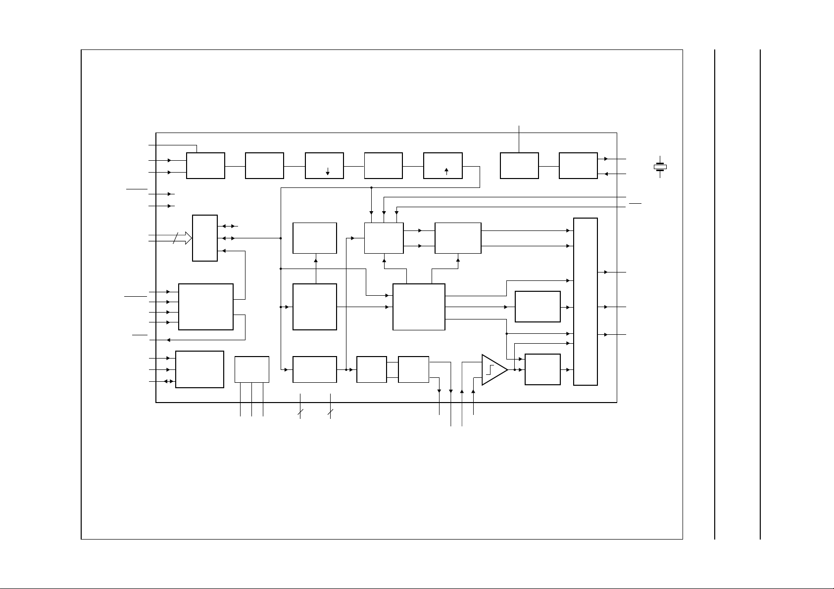
ndbook, full pagewidth
PACLK
BLOCK DIAGRAM
QIC digital equalizer SZA1000
Philips Semiconductors Product specification
V
ref
INA
INB
RESET
TEST
AUXBUS0/WDOUT
AUXBUS1
to
AUXBUS7
WDIN
WGATE
WEQCLK
WEQEN
WGX
SDEN
SCLK
SDIO
37
32
33
30
31
11 to 18
8
10
4
9
3
36
23
24
22
ADC
SZA1000
I/O
MUX
WRITE
EQUALIZATION
SERIAL
INTERFACE
R
ref
HPF
IDAC
38 1 2
IO2IO1
LPF
R
LPF
15 kHz
AMPL.
DETECTOR
DIFF
8, 28,
34, 41
44
V
SSD1VDDD1
V
SSD2VDDD2
V
SSA1VDDA1
V
SSA2VDDA2
5, 26,
35, 42
DAC
FIR
PLL
INTERPOL
AMPL.
QUALIFIER
+
GAP
DETECTOR
LPF
8 MHz
R
MAXIMUM
LIKELIHOOD
DETECTOR
39 44
CMPBEYEA
CMPAEYEB
29
7
CLK
DIV
STRIPE
DETECTOR
READ
PULSE
4340
XOSC/
CLK IN
MUX
MGG582
6
20
19
27
25
21
CLKOUT
CLKIN
RG
LTD
SRD/RD
RRC
GAP/STRIPE
Fig.1 Block diagram.

Philips Semiconductors Product specification
QIC digital equalizer SZA1000
PINNING
SYMBOL PIN DESCRIPTION
IO1 1 programmable current source
IO2 2 programmable current source
WEQEN 3 write equalization circuit enable input
WGATE 4 write gate input; active LOW
V
DDD1
CLKIN 6 external clock or crystal oscillator input
CLKOUT 7 crystal oscillator output
V
SSD1
WEQCLK 9 write equalization circuit clock input
WDIN 10 write equalization circuit data input
AUXBUS0/WDOUT 11 bit 0 auxiliary I/O bus or write equalization output to write amplifier
AUXBUS1 12 bit 1 auxiliary I/O bus
AUXBUS2 13 bit 2 auxiliary I/O bus
AUXBUS3 14 bit 3 auxiliary I/O bus
AUXBUS4 15 bit 4 auxiliary I/O bus
AUXBUS5 16 bit 5 auxiliary I/O bus
AUXBUS6 17 bit 6 auxiliary I/O bus
AUXBUS7 18 bit 7 auxiliary I/O bus
LTD 19 fast lock to data input; active LOW
RG 20 read gate input
GAP/STRIPE 21 gap or stripe detector output
SDIO 22 serial interface data input and output
SDEN 23 serial interface enable input
SCLK 24 serial interface clock input
RRC 25 read reference clock output
V
DDD2
SRD/RD 27 synchronized read data or read data output
V
SSD2
PACLK 29 pre-amp clock output
RESET 30 reset input; active LOW
TEST 31 test input; connect to ground
INA 32 analog signal from read amplifier; positive input
INB 33 analog signal from read amplifier; negative input
V
SSA1
V
DDA1
WGX 36 extended write gate output for floppy tape drives; active LOW
V
ref
R
ref
EYEA 39 differentiated signal; positive output
CMPA 40 comparator for read pulse; positive input
5 digital supply voltage
8 digital ground
26 digital supply voltage
28 digital ground
34 analog ground
35 analog supply voltage
37 positive A/D reference voltage input
38 connect external resistor
1998 Feb 16 4

Philips Semiconductors Product specification
QIC digital equalizer SZA1000
SYMBOL PIN DESCRIPTION
V
SSA2
V
DDA2
CMPB 43 comparator for read pulse; negative input
EYEB 44 differentiated signal; negative output
41 analog ground
42 analog supply voltage
handbook, full pagewidth
IO1
IO2
WEQEN
WGATE
V
DDD1
CLKIN
CLKOUT
V
SSD1
WEQCLK
WDIN
AUXBUS0/WDOUT
EYEB
44
1
2
3
4
5
6
7
8
9
10
11
12
AUXBUS1
DDA2VSSA2
CMPB
V
43
42
13
14
AUXBUS2
AUXBUS3
CMPA
41
40
SZA1000
15
16
AUXBUS4
AUXBUS5
ref
EYEA
R
39
38
17
18
AUXBUS6
AUXBUS7
ref
V
37
19
LTD
WGX
V
36
35
20
21
RG
GAP/STRIPE
DDA1VSSA1
34
22
MGD794
SDIO
33
32
31
30
29
28
27
26
25
24
23
INB
INA
TEST
RESET
PACLK
V
SSD2
SRD/RD
V
DDD2
RRC
SCLK
SDEN
Fig.2 Pin configuration.
1998 Feb 16 5

Philips Semiconductors Product specification
QIC digital equalizer SZA1000
FUNCTIONAL DESCRIPTION
Clock oscillator and divider
The clock source for the SZA1000 can be a crystal
connected between pins 6 and 7, or an external clock
signal connected to pin 6. This clock frequency is divided
by a number programmable between 1 and 8
(see Tables 27 and 28). The resulting frequency, f
, is
s
used as clock input to all on-chip circuits except the write
equalizer. The frequency of the PACLK output signal
(pin 29) is equal to fs.
ADC
The 8-bit ADC has a differential input. The total ADC
conversion range is 1.6 V (p-p; differential). The ADC
sample rate is equal to f
.
s
High-pass filter after the ADC
f
This is a first order filter with a cut-off frequency of
It removes the DC component of the signal.
s
------------ 1608
Low-pass filter
This low-pass filter is an even symmetrical FIR (Finite
Impulse Response) filter. The number of taps depends on
the sample rate reduction factor R (see Tables 30 and 31).
The filter has 8 taps for R = 1 or 14 taps for R = 2 (see
Table 7). The middle taps have a fixed coefficient value of
+128, the coefficients of the other taps are programmable
in the range −128 to +127 (see Table 6).
FIR
This transversal filter has 6 taps with the sample rate equal
to f
(R = 1), or 11 taps with the sample rate equal to1⁄2f
s
(R = 2). Tap 10 has a fixed coefficient value of +64, the
coefficients of the other taps are programmable between
−64 and +63 (see Table 2). The filter has 19 signal delay
sections. The position of each tap can be selected from a
subset of the 20 possible positions (see Tables 3 and 4).
Amplitude detector
This circuit has a separate rectifier and a positive and
negative peak detector.
Typical rise time (0 to 70%) for a normal MFM or
RLL 1,7 code input signal is , typical decay time
(100 to 30%) is programmable between and
1
--- f
s
500
--------- f
s
(see Tables 10 and 11).
The output is an 8-bit number that can be polled via the
serial interface. In addition, the peak-to-peak value is
calculated and filtered by a first order low-pass filter with a
f
cut-off frequency of
s
------------ 3217
Both the filtered and unfiltered amplitudes can be read via
the serial interface (see Table 44) or via the parallel output
bus.
Amplitude qualifier
A peak is considered valid if its amplitude is above a
qualification threshold. Separate qualification thresholds
are used for the positive and negative peaks. Each
threshold is the greater of:
• a programmable level (QUAL_FIX_ POS and
QUAL_FIX_NEG; control register addresses 24 and 25)
• a programmable fraction (
1
⁄2,3⁄8,1⁄4,1⁄8 or 0;
see Tables 9 and 12) of the peak amplitude of the
incoming signal.
Gap detector
s
When the peak-to-peak amplitude of the measured signal
is below a preset limit (GAP_THRESH; control register
address 28), the gap detector output is HIGH, otherwise
LOW (GAP output on pin 21 must be selected; see
Table 22).
400
--------- f
s
Interpolator
1
If a sample rate of
⁄2fs has been selected for the FIR
(R = 2), it is increased once again to fs at the interpolator.
1998 Feb 16 6

Philips Semiconductors Product specification
QIC digital equalizer SZA1000
Stripe detector
This circuit is used to signal the stripes in QIC 3080,
QIC 3095 and TR4 servo formats (STRIPE output on
pin 21 must be selected; see Table 22). A frequency
detector counts the peaks above the qualification
threshold (see Table 29). An input signal containing
frequencies within ±25% of the programmable nominal
frequency will be detected as a stripe. The microcontroller
can then poll the amplitude of the following burst via the
serial interface.
Differentiator
This function is realized by subtracting samples. The delay
between samples is programmable between 1 and 6
periods of f
, split into two parts to provide a balanced
s
delay between the differentiated and non-differentiated
signals (see Tables 24 to 26).
The PLL
This is a fully digital PLL (Phase Lock Loop) with a
programmable nominal frequency (see Tables 35 and 36),
zero phase restart, programmable window shift
(WIN_SHIFT; control register address 42) and a loop filter
with two separate programmable settings.
The maximum likelihood detector
This detector calculates the most likely position of the
peaks in the signal. It checks for (d,k) code constraints,
and for alternating peaks. If an error is detected, the ‘most
likely’ correction is implemented.
Separate corrections can be enabled or disabled.
The SRD output of the maximum likelihood detector is
valid during the rising edge of the RRC signal (see Fig.4).
The maximum likelihood detector is used only to generate
the SRD signal, and not to generate the time continuous
RD pulse.
SRD
handbook, halfpage
RRC
MGG584
Fig.4 SRD/RRC timing.
The PLL output reference clock is the RRC signal (pin 25;
see Table 34). The frequency of this signal is rounded in
time to f
. The PLL is switched to the nominal frequency if
s
RG (pin 20) is LOW, and makes a zero phase restart at the
first detected peak after RG goes HIGH.
The LTD input (pin 19) is used to select between the two
loop filter settings (see Tables 37 to 42). This allows for
fast lock-in during preamble, before switching to a lower
loop bandwidth for maximum data reliability (see Fig.3).
INPUT
handbook, halfpage
SIGNALS
RG
LTD
PLL
MODE
nominal
frequency
preamble
zero phase restart
fast lock-in normal read mode
data
MGG583
Fig.3 PLL timing diagram.
The DAC
This is an internal differential 8-bit DAC operating at f
.
s
The LPF after the DAC
This analog LPF filters the time quantized signal from the
DAC to retain a time continuous signal. This provides more
accurate timing of the detected zero crossings in the RD
pulse output.
The LPF is a second order active filter with a cut-off
frequency of 8 MHz.
The read pulse circuit
A peak in the equalized signal at the interpolator output
generates a read pulse. The peak is detected if a zero
crossing occurs in the filtered signal after the DAC while
the non-differentiated signal is above the qualification
threshold.
Uncommitted current sources
Two uncommitted 5-bit programmable current sink DACs
(0 to 2 mA) are available as IO1 and IO2 (see Table 20 for
programming). These could be used, for example, to drive
the tape hole detector circuit.
1998 Feb 16 7

Philips Semiconductors Product specification
QIC digital equalizer SZA1000
Parallel state bus
All internal digital signals can be monitored via an 8-bit
parallel bus. An external DAC or an evaluation tool such as
a phase error logger for TIA (Time Interval Analyzer),
drop-out and symmetry measurements can be connected
to this bus for evaluation purposes (see Table 34).
Write equalization
This circuit has an independent clock input WEQCLK at
pin 9.
Write equalization can be programmed to conform to a
number of formats including QIC 3010, QIC 3020,
QIC 3080, QIC 3095, QIC 5010, Travan 2, Travan 3 and
Travan 4.
This is achieved by programming the circuit to divide a
channel bit-cell into 2, 3 or 6 time slots (see Tables 13
and 14). The external WEQ clock frequency should be
selected such that an integer number of between 1 and 8
clock periods fits in a time slot (see Tables 18 and 19).
The width and position of the inserted write pulse can be
programmed (see Tables 15 to 17).
The write equalization circuit input and output signals can
be independently programmed to be in either WD or WDI
format (see Table 15).
For QIC 3010 or 3020, the recording signal is typically
generated by a circuit that uses a separate crystal.
An input buffer with variable delay is used to prevent errors
occurring in the recorded signal. This buffer is set to its
nominal position when writing begins.
Signals longer than a data block can be recorded during
formatting. To avoid overloading the time buffer, the circuit
can resynchronize automatically during gaps in the
QIC 3010 or 3020 format.
Serial interface
The serial interface uses 8-bit addresses and 8-bit data.
Its timing is shown in Fig.5. IC mode settings, filter
coefficients, scale factors and thresholds can be loaded
via the serial interface.
Measured signal amplitude, for example Burst level
measurement at QIC 3095 or AGC control by the
microcontroller, and the actual PLL frequency can be read
via the serial interface. To read data from the status
registers, hex address FF must be transmitted along with
the required data code. The IC will then respond with the
contents of the appropriate 8-bit status register
(see Table 44).
1998 Feb 16 8

This text is here in white to force landscape pages to be rotated correctly when browsing through the pdf in the Acrobat reader.This text is here in
k
_white to force landscape pages to be rotated correctly when browsing through the pdf in the Acrobat reader.This text is here inThis text is here in
white to force landscape pages to be rotated correctly when browsing through the pdf in the Acrobat reader. white to force landscape pages to be ...
1998 Feb 16 9
WRITE SETTINGS
SDEN
SCLK
, full pagewidth
Philips Semiconductors Product specification
QIC digital equalizer SZA1000
SDIO
SDEN
SCLK
SDIO
A7 A6 A5 A4 A3 A2 A1 A0 D7 D6 D5 D4 D3 D2 D1 D0
READ STATUS
A7 A6 A5 A4 A3 A2 A1 A0 D7 D6 D5 D4 D3 D2 D1 D0 D7 D6 D5 D4 D3 D2 D1 D0
ADDRESS AND DATA FROM MICROCONTROLLER DATA OUT FROM DEVICE
3-STATE
3-STATE
MGG585
Fig.5 Serial I/O timing diagrams.

Philips Semiconductors Product specification
QIC digital equalizer SZA1000
CONTROL REGISTER
Control register settings
The control register is accessible through the serial interface and contains 46 8-bit entries as shown in Table 1.
Table 1 Control register
ADDRESS NAME DESCRIPTION
0 FIR_VAL0 FIR tap 0 coefficient value (see Table 2)
1 FIR_VAL1 FIR tap 1 coefficient value
2 FIR_VAL2 FIR tap 2 coefficient value
3 FIR_VAL3 FIR tap 3 coefficient value
4 FIR_VAL4 FIR tap 4 coefficient value
5 FIR_VAL5 FIR tap 5 coefficient value
6 FIR_VAL6 FIR tap 6 coefficient value
7 FIR_VAL7 FIR tap 7 coefficient value
8 FIR_VAL8 FIR tap 8 coefficient value
9 FIR_VAL9 FIR tap 9 coefficient value
10 FIR_SEL05 FIR tap positions (see Tables 3 and 4)
11 FIR_SEL16 FIR tap positions
12 FIR_SEL27 FIR tap positions
13 FIR_SEL38 FIR tap positions
14 FIR_SEL49 FIR tap positions
15 FIR_SEL10 FIR tap positions
16 FIR_SHIFT FIR output scaling (see Table 5)
17 LPF_VAL1 LPF tap coefficient value (see Table 6)
18 LPF_VAL4 LPF tap coefficient value
19 LPF_VAL2 LPF tap coefficient value
20 LPF_VAL5 LPF tap coefficient value
21 LPF_VAL3 LPF tap coefficient value
22 LPF_VAL6 LPF tap coefficient value
23 LPF_SHIFT LPF output scaling (see Table 8)
24 QUAL_FIX_POS Amplitude qualifier positive fixed qualification threshold
25 QUAL_FIX_NEG Amplitude qualifier negative fixed qualification threshold
26 QUAL_VAR_GAIN Amplitude qualifier variable gain factors (see Tables 9 and 12)
27 QUAL_SLOPE_DEL Amplitude detector slope qualification delay (see Table 10)
28 GAP_THRESH Gap detector fixed threshold
29 WEQ_SET0 WEQ settings (see Tables 13 and 14)
30 WEQ_SET1 WEQ settings (see Tables 15, 16 and 17)
31 WEQ_CLK_DIV WEQ clock divider (see Tables 18 and 19)
32 − not used
33 IDAC1 IO1 DAC current (see Table 20)
34 IDAC2 IO2 DAC current (see Table 20)
1998 Feb 16 10
 Loading...