

Philips SK6.0A CA Schematic

Colour Television Chassis
SK6.0A
CA
H_17230_000.eps
290607
Contents Page Contents Page
1. Technical Specifications, Connections, and Chassis
Overview 2
2. Safety Instructions, Warnings, and Notes 4
3. Directions for Use 6
4. Mechanical Instructions 7
5. Service Modes, Error Codes, and Fault Finding 9
6. Block Diagrams, Test Point Overviews, and
Waveforms
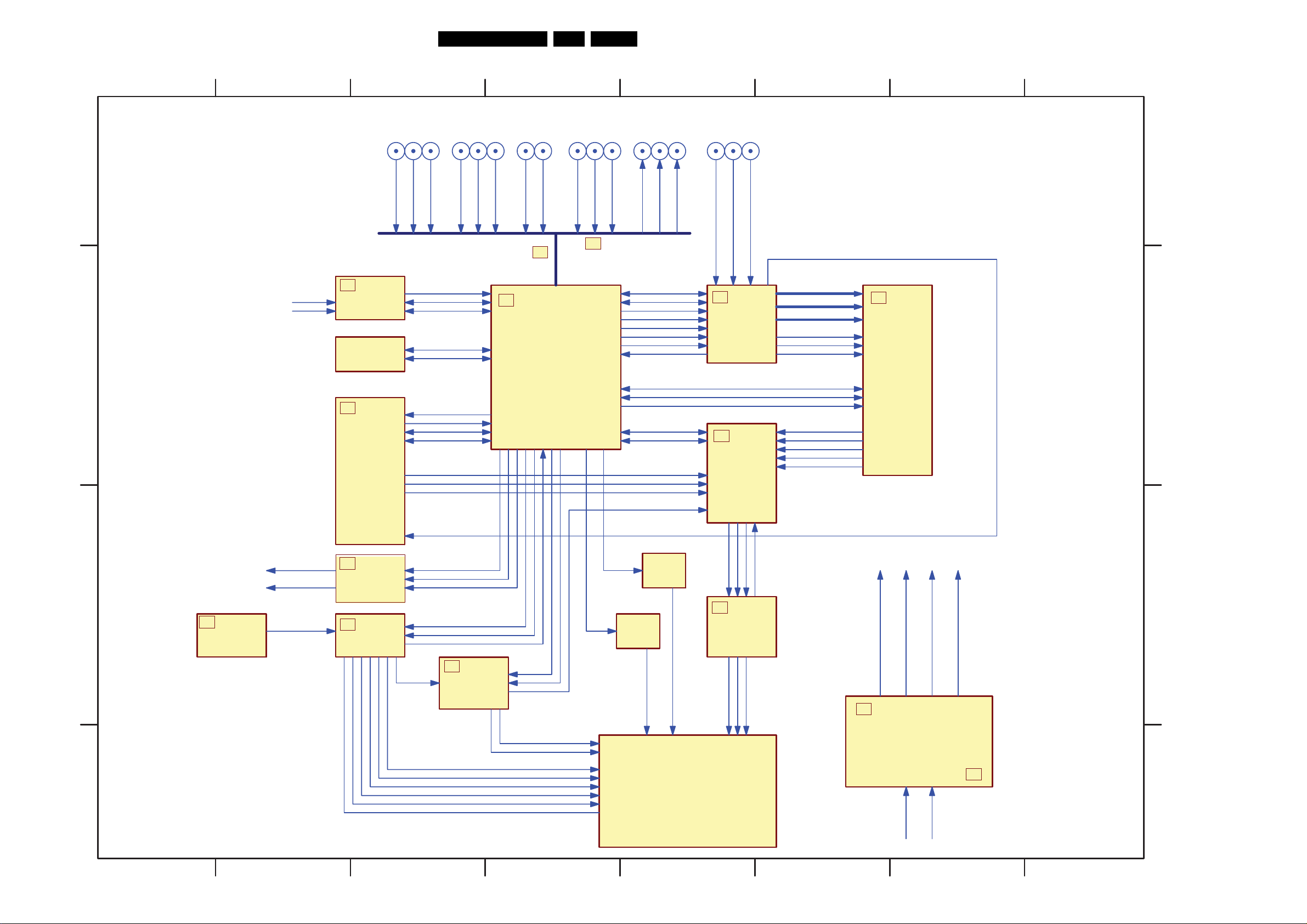
Block Diagram Digital Board 100Hz 11
Block Diagram Chassis (Digital Board 100Hz) 12
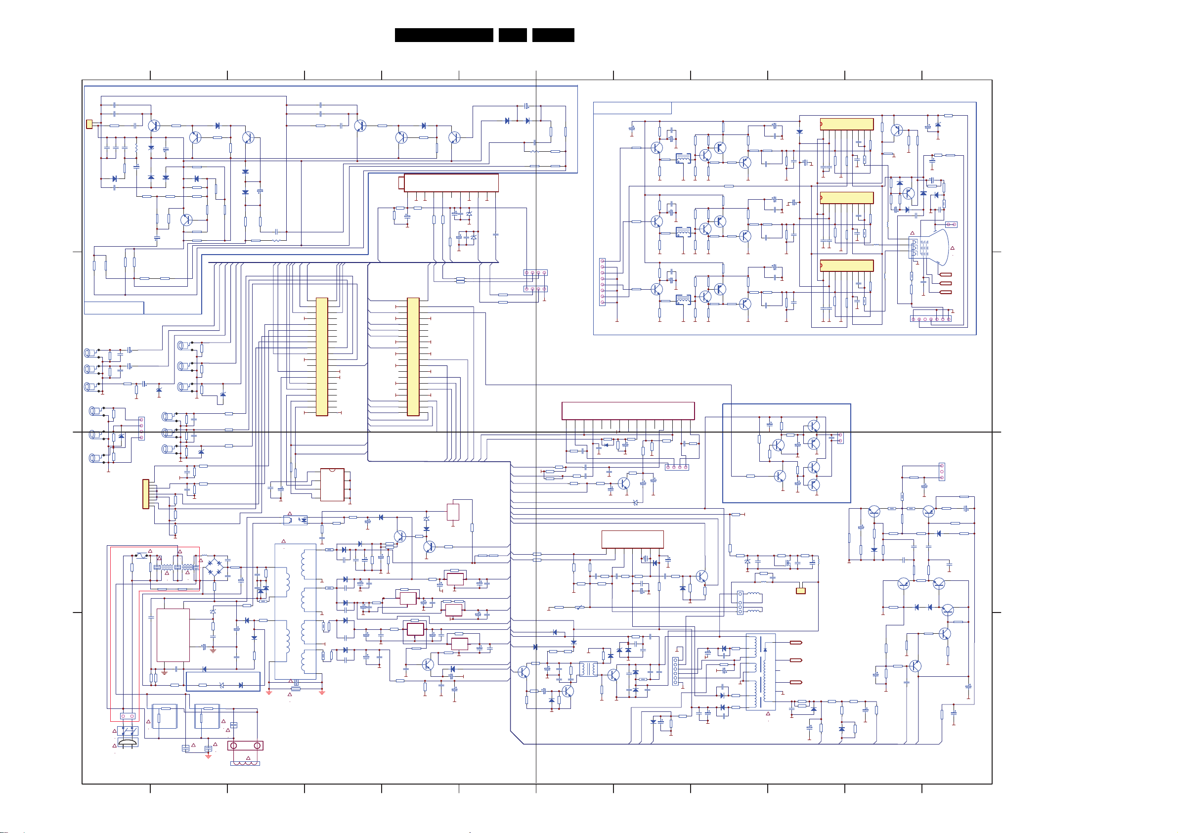
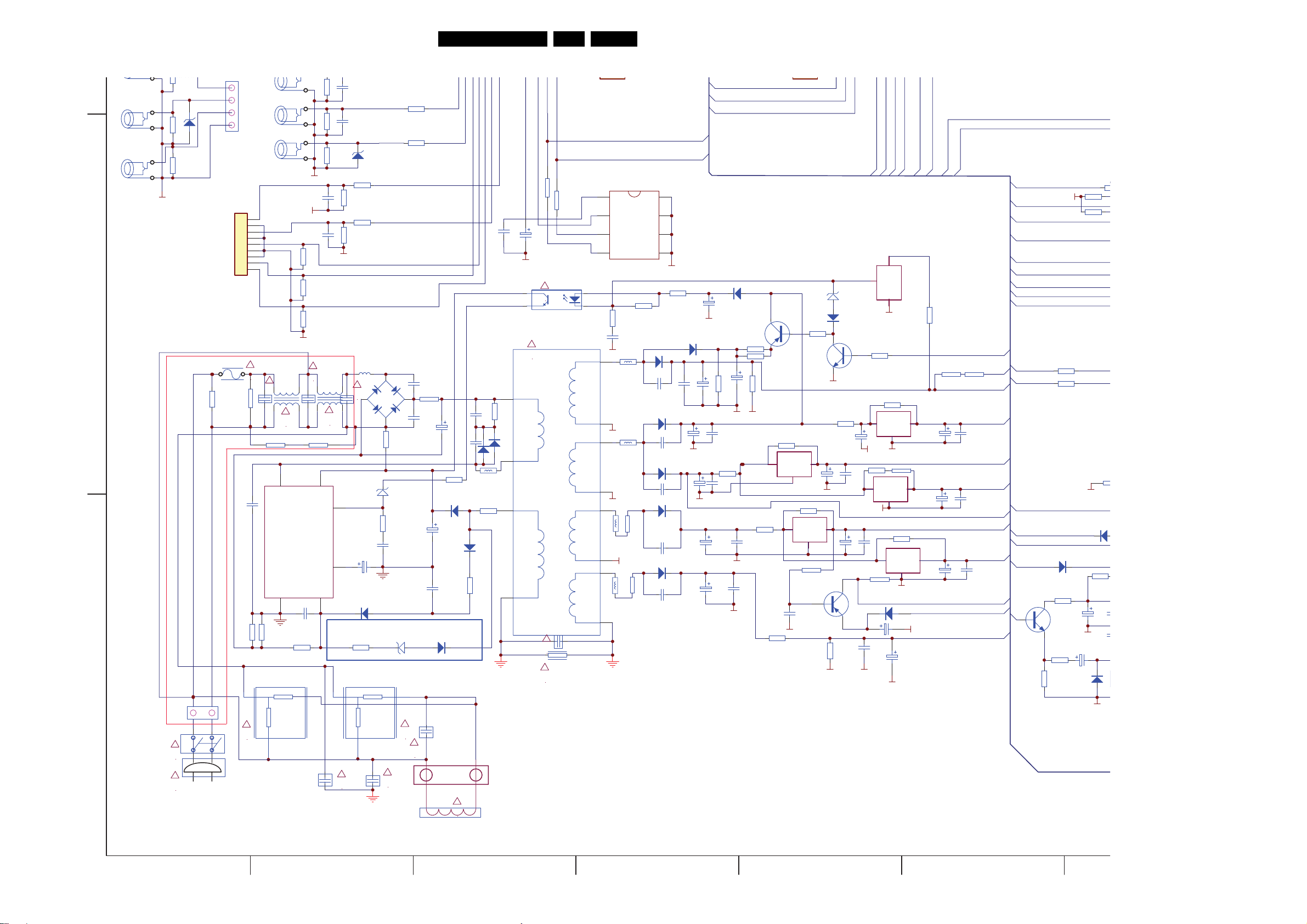
Schematic Diagram Chassis (Overview) 13
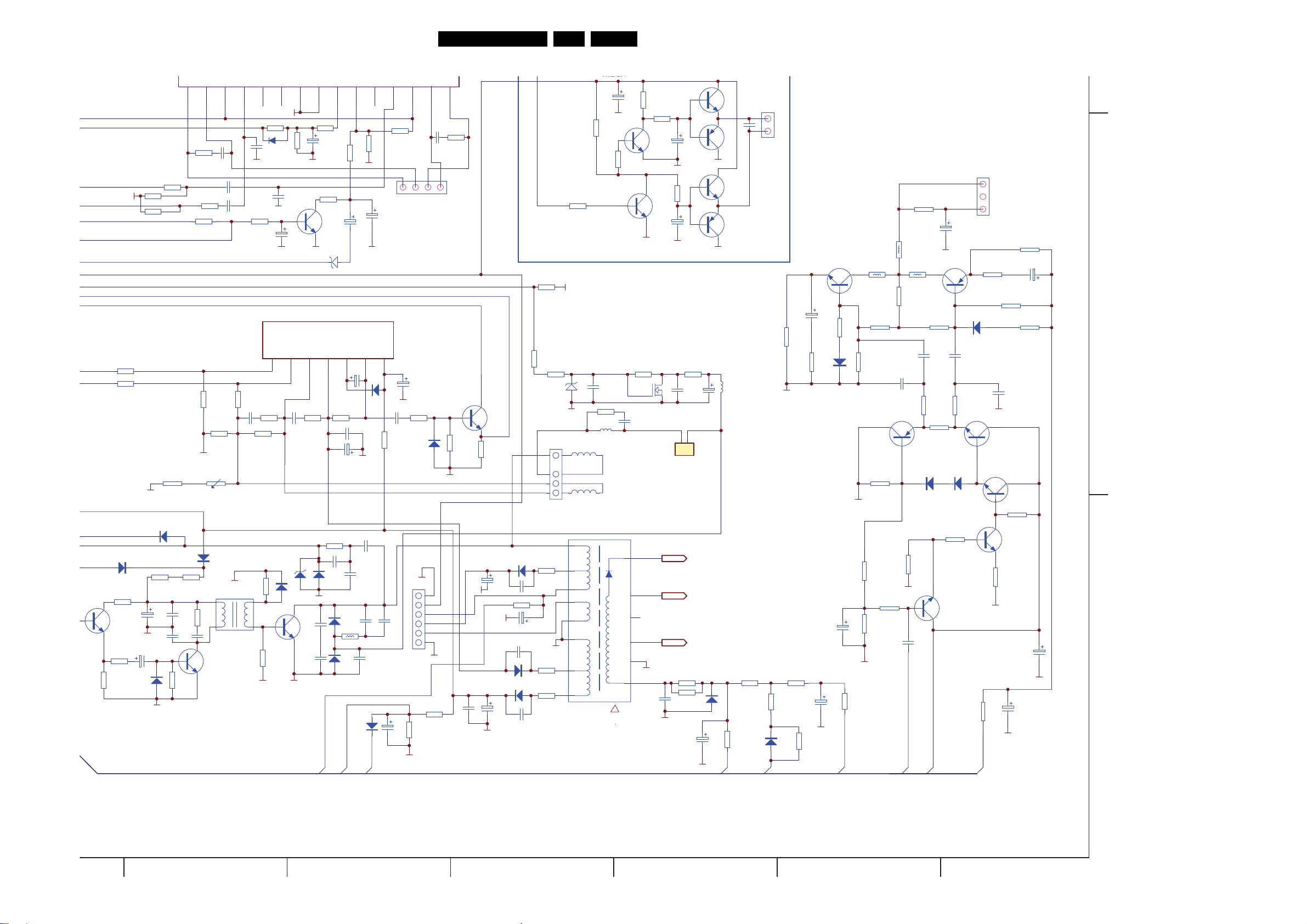
Schematic Diagram Chassis (Part 1) 14
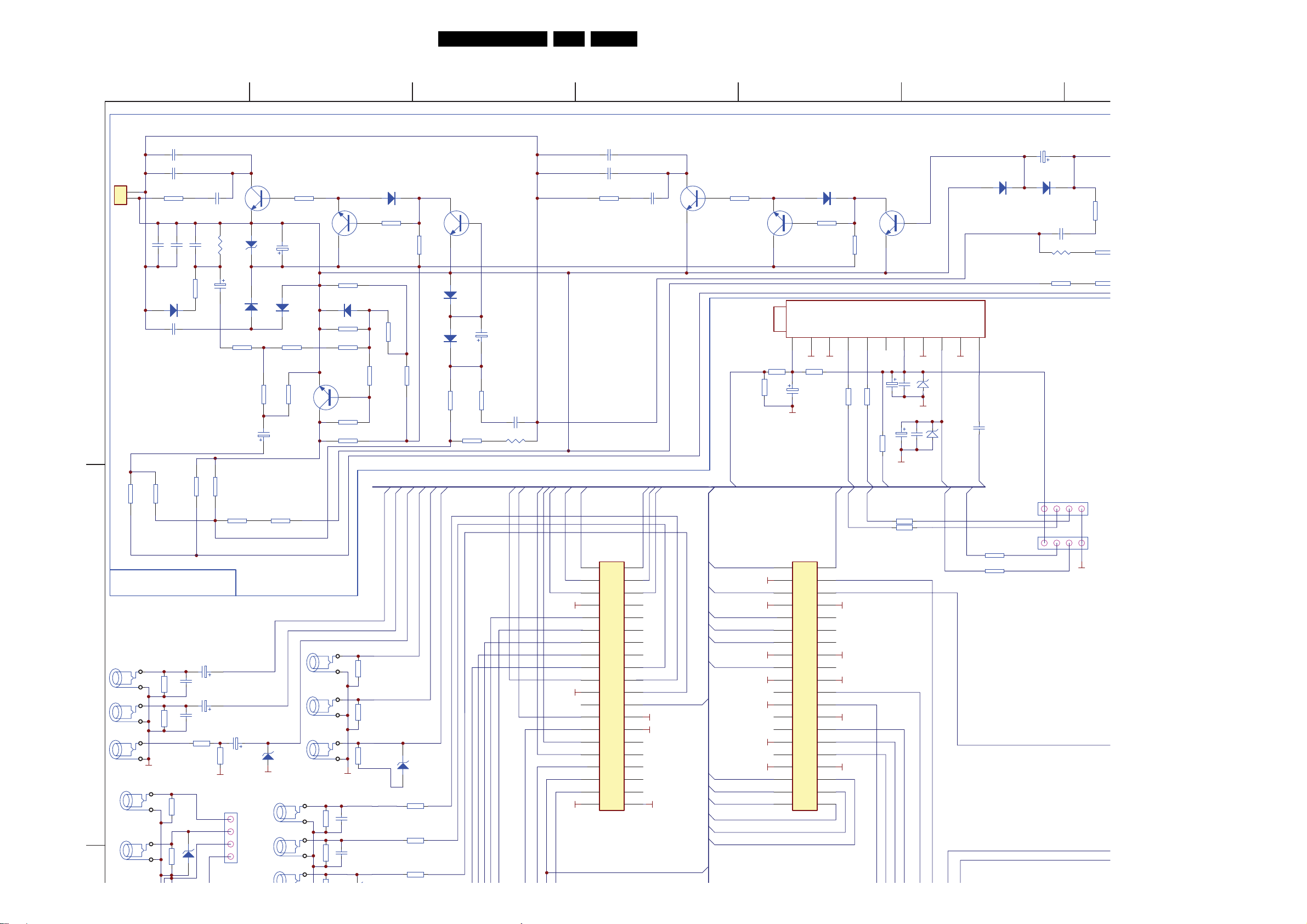
Schematic Diagram Chassis (Part 2) 15
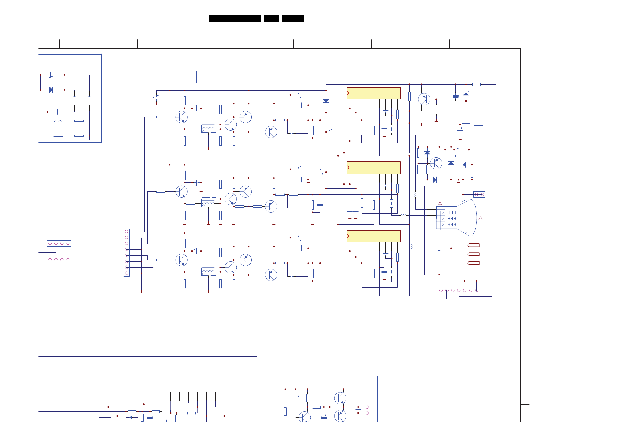
Schematic Diagram Chassis (Part 3) 16
Schematic Diagram Chassis (Part 4) 17
7. Circuit Diagrams and PWB Layouts
Mono Carrier: Power Supply (A1) 18 25-26
Mono Carrier: Line Deflection (A2) 19 25-26
Mono Carrier: Frame Deflection (A3) 20 25-26
Mono Carrier: Tuner IF (A4) 21 25-26
Mono Carrier: AV I/O Interface (A5) 22 25-26
Mono Carrier: Audio Amplifier (A6) 23 25-26
Mono Carrier: Digital Interface Circuit (A7) 24 25-26
CRT Amplifier Circuit (B) 27 28
Digital Board: Display Processor (C1) 29 36-37
Digital Board: Scaler (Part 1) (C2) 30 36-37
Digital Board: Scaler (Part 2) (C2) 31 36-37
Digital Board: 8-Bit Processor (OSD) (C3) 32 36-37
Digital Board: UOC III (C4) 33 36-37
Digital Board: AD Converter (C5) 34 36-37
Digital Board: Interface (C5) 35 36-37
Front Control (D) 38 39
Mains Filter Panel (E) 40 41
Side A/V Panel (G) 42 43
©
Copyright 2007 Philips Consumer Electronics B.V. Eindhoven, The Netherlands.
All rights reserved. No part of this publication may be reproduced, stored in a
retrieval system or transmitted, in any form or by any means, electronic,
mechanical, photocopying, or otherwise without the prior permission of Philips.
Slim Panel (M) 44 45
8. Alignments 47
9. Circuit Descriptions, Abbreviation List, and IC Data
Sheets 51
Abbreviation List 51
IC Data Sheets 53
10. Spare Parts List 66
11. Revision List 71
Published by JY 0768 BU CD Customer Service Printed in the Netherlands Subject to modification EN 3122 785 17231
EN 2 SK6.0A CA1.
Technical Specifications, Connections, and Chassis Overview
1. Technical Specifications, Connections, and Chassis Overview
Index of this chapter:
1.1 Technical Specifications
1.2 Connection Overview
1.3 Chassis Overview
Note: Data below can deviate slightly from the actual situation,
due to the different set executions.
1.1 Technical Specifications
1.1.1 Vision
Display type : CRT
Screen size : 29” (72 cm), 4:3
Tuning system : VST/PLL
TV Colour systems : PAL D/K and I
Video playback : NTSC M/N 3.58, 4.43
: PAL 50
Presets/channels : 256 channels
Tuner bands : VHF
: UHF
1.1.2 Sound
Sound systems : FM-stereo
: AV Bi-sonic stereo
Maximum power (W
1.1.3 Miscellaneous
):2 x 6
RMS
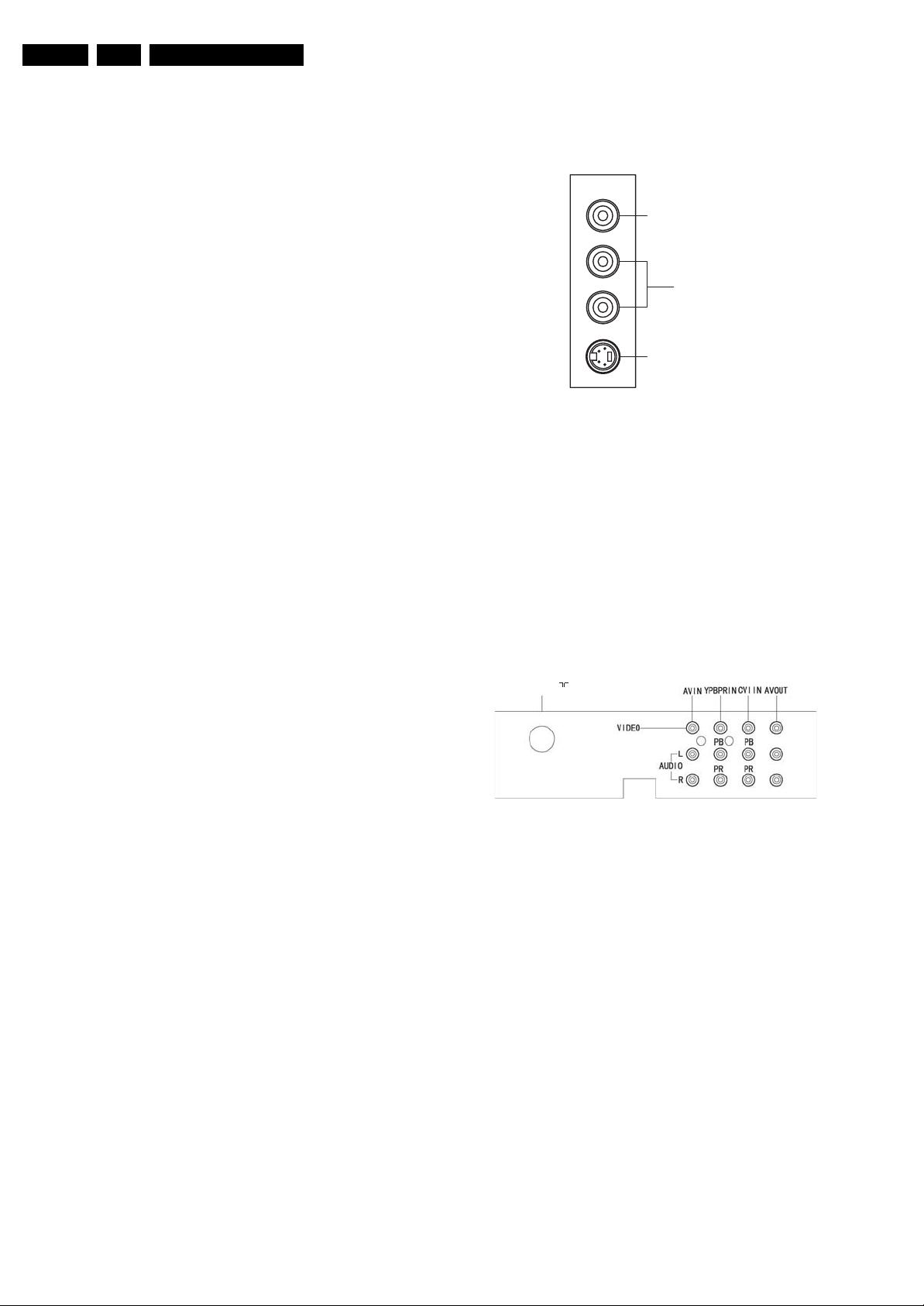
1.2.1 Side Connections
VIDEO
L
AUDIO
R
S-VIDEO
G_16540_034.eps
290607
Figure 1-1 Side I/O connections
Cinch: Video CVBS - In, Audio - In
Ye - Video CVBS 1 V
Wh - Audio L 0.5 V
Rd - Audio R 0.5 V
/ 75 ohm jq
PP
/ 10 kohm jq
RMS
/ 10 kohm jq
RMS
S-Video (Hosiden): Video Y/C - In
1 - Ground Y Gnd H
2 - Ground C Gnd H
3 -Video Y 1 V
4 - Video C 0.3 V
/ 75 ohm j
PP
P / 75 ohm j
PP
Power supply:
- Mains voltage (V
) : 160 - 260
AC
- Mains frequency (Hz) : 50 / 60
Ambient conditions:
- Temperature range (°C) : -5 to +45
- Maximum humidity : 90% R.H.
Power consumption
- Normal operation (W) : ≈ 150
- Stand-by (W) : < 3
1.2 Connection Overview
Note: The following connector colour abbreviations are used
(according to DIN/IEC 757): Bk= Black, Bu= Blue, Gn= Green,
Gy= Grey, Rd= Red, Wh= White, and Ye= Yellow.
1.2.2 Rear Connections
75 Ohm
Figure 1-2 Rear connections
Aerial - In
- - IEC-type (EU) Coax, 75 ohm D
Cinch: Video CVBS - In, Audio - In
Ye - Video CVBS 1 V
Wh - Audio L 0.5 V
Rd - Audio R 0.5 V
/ 75 ohm jq
PP
/ 10 kohm jq
RMS
/ 10 kohm jq
RMS
Cinch: Video YPbPr - In
Gn - Video Y 1 V
Bu - Video Pb 0.7 V
Rd - Video Pr 0.7 V
/ 75 ohm jq
PP
/ 75 ohm jq
PP
/ 75 ohm jq
PP
Cinch: Video CVBS - Out, Audio - Out
Ye - Video CVBS 1 V
Wh - Audio L 0.5 V
Rd - Audio R 0.5 V
/ 75 ohm kq
PP
/10 kohm kq
RMS
/ 10 kohm kq
RMS
G_16550_028.eps
051006
Technical Specifications, Connections, and Chassis Overview
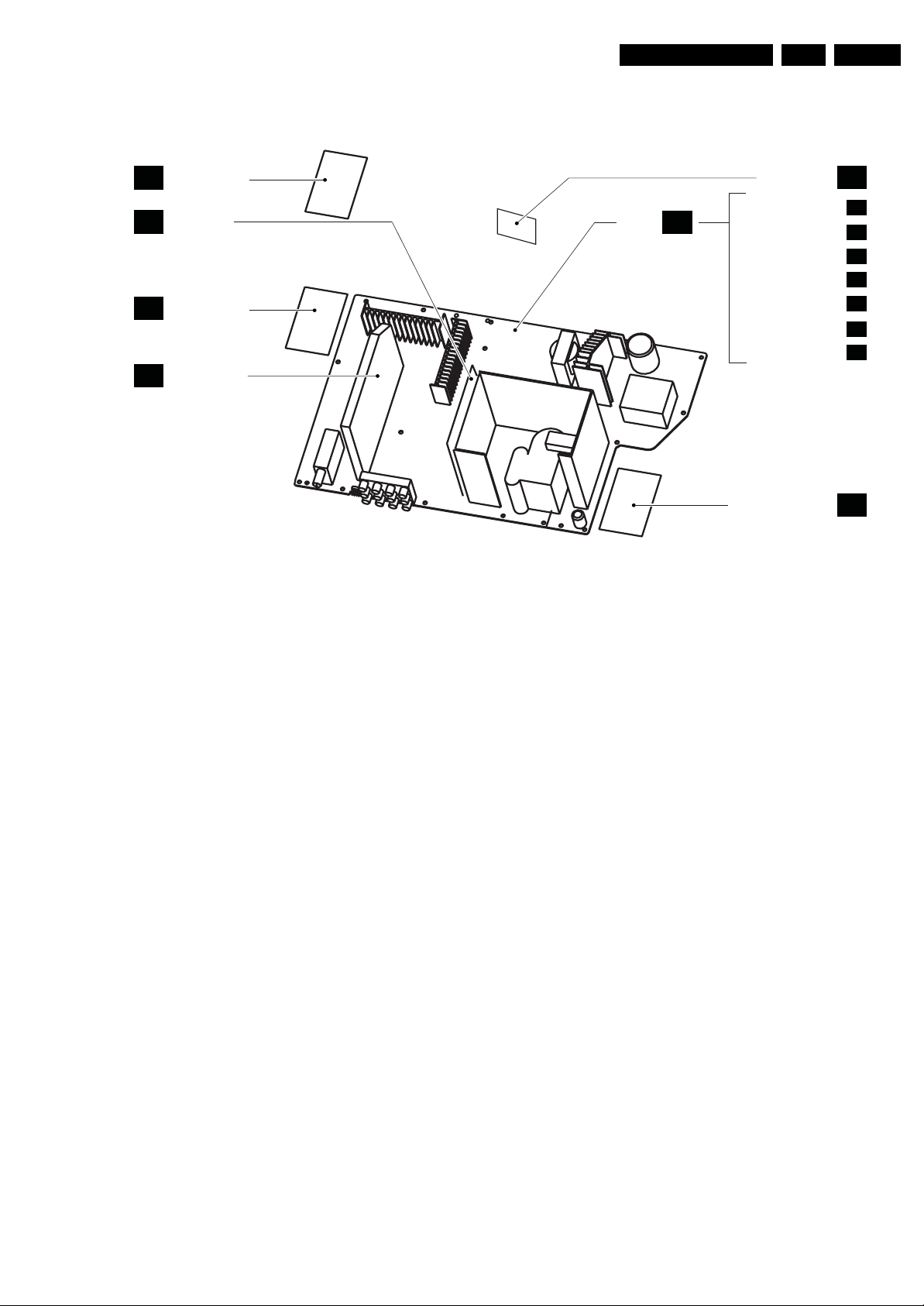
1.3 Chassis Overview
EN 3SK6.0A CA 1.
6,'($93$1(/
G
6/,03$1(/
M
0$,16),/7(5
E
3$1(/
+]%2$5'
C
Figure 1-3 PWB location
0212
&$55,(5
A
&57 3$1(/
32:(5 6833/<
/,1( '()/(&7,21
)5$0( '()/(&7,21
781(5 ,)
$9 ,2
$8',2 $03/,),(5
',*,7$/,17(5)$&(
)5217&21752/
H_17230_025.eps
B
A1
A2
A3
A4
A5
A6
A7
D
290607
EN 4 SK6.0A CA2.
Safety Instructions, Warnings, and Notes
2. Safety Instructions, Warnings, and Notes
Index of this chapter:
2.1 Safety Instructions
2.2 Maintenance Instructions
2.3 Warnings
2.4 Notes
2.1 Safety Instructions
Safety regulations require the following during a repair:
• Connect the set to the Mains/AC Power via an isolation
transformer (> 800 VA).
• Replace safety components, indicated by the symbol h,
only by components identical to the original ones. Any
other component substitution (other than original type) may
increase risk of fire or electrical shock hazard.
• Wear safety goggles when you replace the CRT.
Safety regulations require that after a repair, the set must be
returned in its original condition. Pay in particular attention to
the following points:
• General repair instruction: as a strict precaution, we advise
you to re-solder the solder connections through which the
horizontal deflection current flows. In particular this is valid
for the:
1. Pins of the line output transformer (LOT).
2. Fly-back capacitor(s).
3. S-correction capacitor(s).
4. Line output transistor.
5. Pins of the connector with wires to the deflection coil.
6. Other components through which the deflection current
flows.
Note: This re-soldering is advised to prevent bad connections
due to metal fatigue in solder connections, and is therefore only
necessary for television sets more than two years old.
• Route the wire trees and EHT cable correctly and secure
them with the mounted cable clamps.
• Check the insulation of the Mains/AC Power lead for
external damage.
• Check the strain relief of the Mains/AC Power cord for
proper function, to prevent the cord from touching the CRT,
hot components, or heat sinks.
• Check the electrical DC resistance between the Mains/AC
Power plug and the secondary side (only for sets that have
a Mains/AC Power isolated power supply):
1. Unplug the Mains/AC Power cord and connect a wire
between the two pins of the Mains/AC Power plug.
2. Set the Mains/AC Power switch to the “on” position
(keep the Mains/AC Power cord unplugged!).
3. Measure the resistance value between the pins of the
Mains/AC Power plug and the metal shielding of the
tuner or the aerial connection on the set. The reading
should be between 4.5 Mohm and 12 Mohm.
4. Switch “off” the set, and remove the wire between the
two pins of the Mains/AC Power plug.
• Check the cabinet for defects, to prevent touching of any
inner parts by the customer.
2.2 Maintenance Instructions
We recommend a maintenance inspection carried out by
qualified service personnel. The interval depends on the usage
conditions:
• When a customer uses the set under normal
circumstances, for example in a living room, the
recommended interval is three to five years.
• When a customer uses the set in an environment with
higher dust, grease, or moisture levels, for example in a
kitchen, the recommended interval is one year.
• The maintenance inspection includes the following actions:
1. Perform the “general repair instruction” noted above.
2. Clean the power supply and deflection circuitry on the
chassis.
3. Clean the picture tube panel and the neck of the picture
tube.
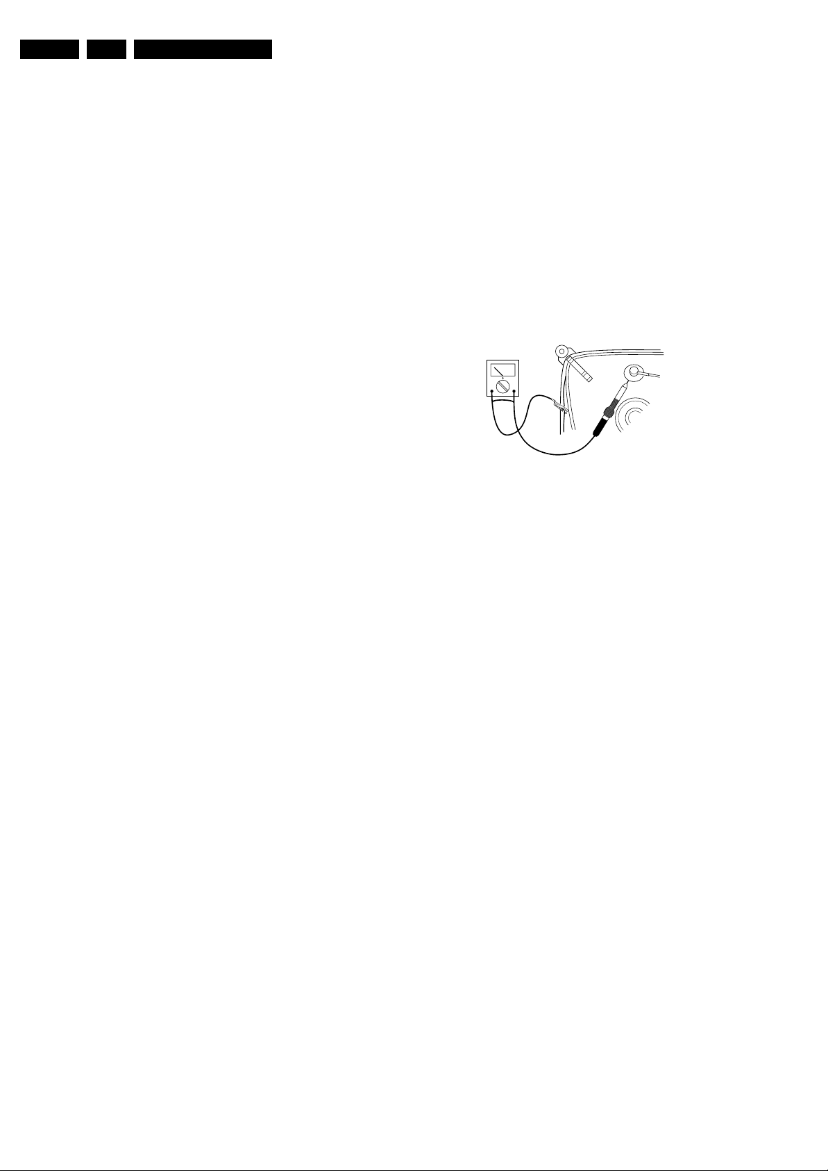
2.3 Warnings
• In order to prevent damage to ICs and transistors, avoid all
high voltage flashovers. In order to prevent damage to the
picture tube, use the method shown in figure “Discharge
picture tube”, to discharge the picture tube. Use a high
voltage probe and a multi-meter (position V
until the meter reading is 0 V (after approx. 30 s).
V
E_06532_007.eps
250304
Figure 2-1 Discharge picture tube
• All ICs and many other semiconductors are susceptible to
electrostatic discharges (ESD w). Careless handling
during repair can reduce life drastically. Make sure that,
during repair, you are connected with the same potential as
the mass of the set by a wristband with resistance. Keep
components and tools also at this same potential.
• Be careful during measurements in the high voltage
section.
• Never replace modules or other components while the unit
is switched “on”.
• When you align the set, use plastic rather than metal tools.
This will prevent any short circuits and prevents circuits
from becoming unstable.
2.4 Notes
2.4.1 General
• Measure the voltages and waveforms with regard to the
chassis (= tuner) ground (H), or hot ground (I), depending
on the tested area of circuitry. The voltages and waveforms
shown in the diagrams are indicative. Measure them in the
Service Default Mode (see chapter 5) with a colour bar
signal and stereo sound (L: 3 kHz, R: 1 kHz unless stated
otherwise) and picture carrier at 475.25 MHz for PAL, or
61.25 MHz for NTSC (channel 3).
• Where necessary, measure the waveforms and voltages
with (D) and without (E) aerial signal. Measure the
voltages in the power supply section both in normal
operation (G) and in stand-by (F). These values are
indicated by means of the appropriate symbols.
• The semiconductors indicated in the circuit diagram and in
the parts lists, are interchangeable per position with the
semiconductors in the unit, irrespective of the type
indication on these semiconductors.
• Manufactured under license from Dolby Laboratories.
“Dolby”, “Pro Logic” and the “double-D symbol”, are
trademarks of Dolby Laboratories.
). Discharge
DC
Safety Instructions, Warnings, and Notes
EN 5SK6.0A CA 2.
2.4.2 Schematic Notes
• All resistor values are in ohms, and the value multiplier is
often used to indicate the decimal point location (e.g. 2K2
indicates 2.2 kohm).
• Resistor values with no multiplier may be indicated with
either an “E” or an “R” (e.g. 220E or 220R indicates 220
ohm).
• All capacitor values are given in micro-farads (μ= x10
nano-farads (n= x10
-9
), or pico-farads (p= x10
• Capacitor values may also use the value multiplier as the
decimal point indication (e.g. 2p2 indicates 2.2 pF).
• An “asterisk” (*) indicates component usage varies. Refer
to the diversity tables for the correct values.
• The correct component values are listed in the Spare Parts
List. Therefore, always check this list when there is any
doubt.
2.4.3 Lead-free Soldering
Due to lead-free technology some rules have to be respected
by the workshop during a repair:
• Use only lead-free soldering tin Philips SAC305 with order
code 0622 149 00106. If lead-free solder paste is required,
please contact the manufacturer of your soldering
equipment. In general, use of solder paste within
workshops should be avoided because paste is not easy to
store and to handle.
• Use only adequate solder tools applicable for lead-free
soldering tin. The solder tool must be able:
– To reach a solder-tip temperature of at least 400°C.
– To stabilize the adjusted temperature at the solder-tip.
– To exchange solder-tips for different applications.
• Adjust your solder tool so that a temperature of around
360°C - 380°C is reached and stabilized at the solder joint.
Heating time of the solder-joint should not exceed ~ 4 sec.
Avoid temperatures above 400°C, otherwise wear-out of
tips will increase drastically and flux-fluid will be destroyed.
To avoid wear-out of tips, switch “off” unused equipment or
reduce heat.
• Mix of lead-free soldering tin/parts with leaded soldering
tin/parts is possible but PHILIPS recommends strongly to
avoid mixed regimes. If this cannot be avoided, carefully
clear the solder-joint from old tin and re-solder with new tin.
-12
example below it is 2006 week 17). The 6 last digits contain the
serial number.
MODEL :
PROD.NO:
-6
),
32PF9968/10
AG 1A0617 000001
).
MADE IN BELGIUM
220-240V 50/60Hz
~
VHF+S+H+UHF
BJ3.0E LA
S
128W
E_06532_024.eps
130606
Figure 2-2 Serial number (example)
2.4.5 Board Level Repair (BLR) or Component Level Repair (CLR)
If a board is defective, consult your repair procedure to decide
if the board has to be exchanged or if it should be repaired on
component level.
If your repair procedure says the board should be exchanged
completely, do not solder on the defective board. Otherwise, it
cannot be returned to the O.E.M. supplier for back charging!
2.4.6 Practical Service Precautions
• It makes sense to avoid exposure to electrical shock.
While some sources are expected to have a possible
dangerous impact, others of quite high potential are of
limited current and are sometimes held in less regard.
• Always respect voltages. While some may not be
dangerous in themselves, they can cause unexpected
reactions that are best avoided. Before reaching into a
powered TV set, it is best to test the high voltage insulation.
It is easy to do, and is a good service precaution.
2.4.4 Alternative BOM identification
The third digit in the serial number (example:
AG2B0335000001) indicates the number of the alternative
B.O.M. (Bill Of Materials) that has been used for producing the
specific TV set. In general, it is possible that the same TV
model on the market is produced with e.g. two different types
of displays, coming from two different suppliers. This will then
result in sets which have the same CTN (Commercial Type
Number; e.g. 28PW9515/12) but which have a different B.O.M.
number.
By looking at the third digit of the serial number, one can
identify which B.O.M. is used for the TV set he is working with.
If the third digit of the serial number contains the number “1”
(example: AG1B033500001), then the TV set has been
manufactured according to B.O.M. number 1. If the third digit is
a “2” (example: AG2B0335000001), then the set has been
produced according to B.O.M. no. 2. This is important for
ordering the correct spare parts!
For the third digit, the numbers 1...9 and the characters A...Z
can be used, so in total: 9 plus 26= 35 different B.O.M.s can be
indicated by the third digit of the serial number.
Identification: The bottom line of a type plate gives a 14-digit
serial number. Digits 1 and 2 refer to the production centre (e.g.
AG is Bruges), digit 3 refers to the B.O.M. code, digit 4 refers
to the Service version change code, digits 5 and 6 refer to the
production year, and digits 7 and 8 refer to production week (in

EN 6 SK6.0A CA3.
3. Directions for Use
You can download this information from the following websites:
http://www.philips.com/support
http://www.p4c.philips.com
Directions for Use
4. Mechanical Instructions
Mechanical Instructions
EN 7SK6.0A CA 4.
Index of this chapter:
4.1 Set Disassembly
4.2 Assembly / Board Removal
4.3 Set Re-assembly
Note: Figures below can deviate slightly from the actual
situation, due to the different set executions.
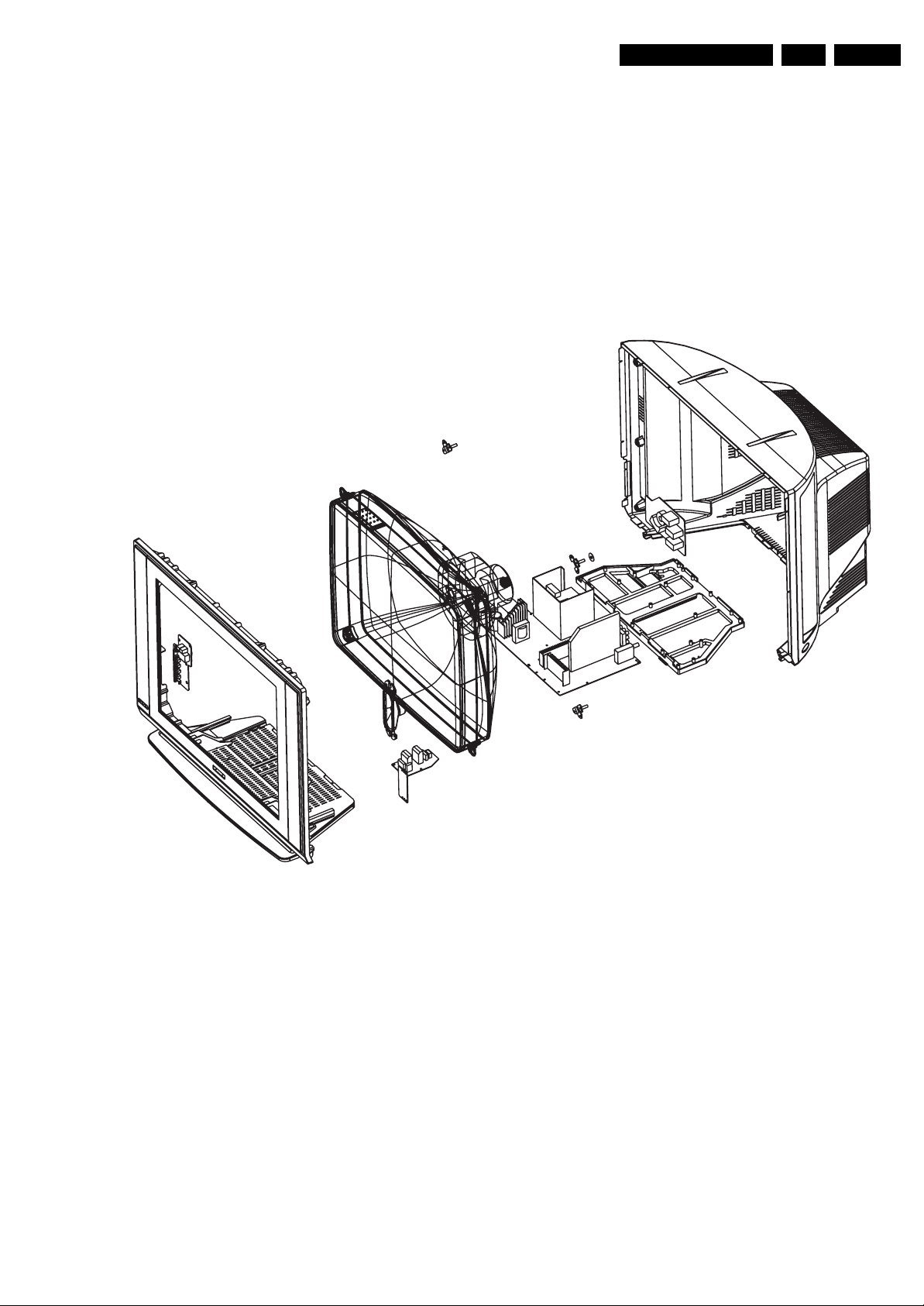
4.1 Set Disassembly
Follow the disassemble instructions in described order.
4.1.1 Rear Cover Removal
Warning: disconnect the mains power cord before you remove
the rear cover.
1. Remove all the fixation screws of the rear cover.
2. Now, pull the rear cover backwards and remove it.
Figure 4-1 Rear Cover removal
H_17230_026.eps
290607
EN 8 SK6.0A CA4.
Mechanical Instructions
4.2 Assembly / Board Removal
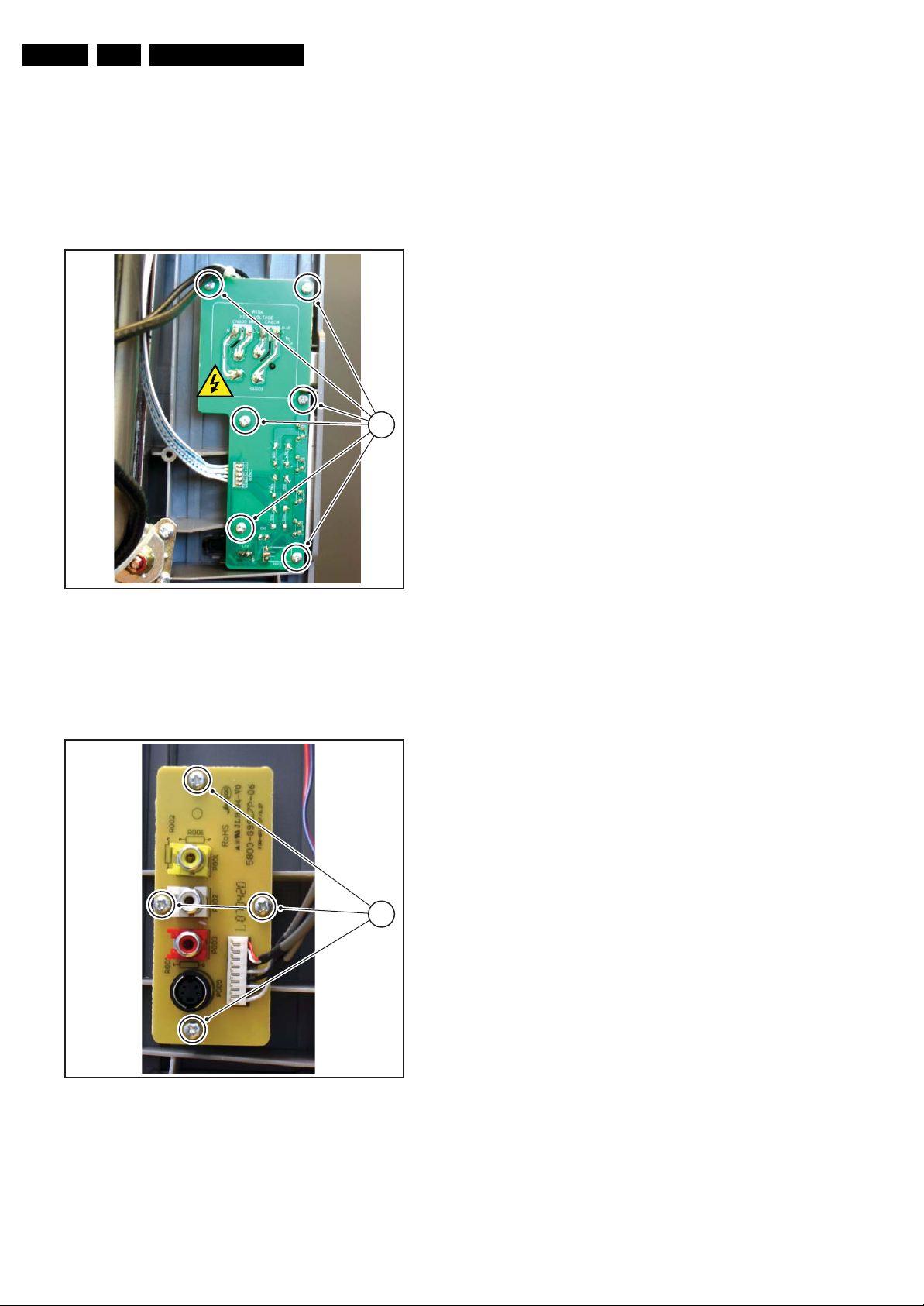
4.2.1 Power Switch and Control Panel removal
1. From the mono carrier disconnect the main power and the
keyboard circuit cables. Release the main power cord and
the keyboard circuit cable from it’s strain reliefs.
2. Then, remove the six fixation screws [1] of the power
switch and control panel and remove the board.
4.3 Set Re-assembly
To re-assemble the whole set, do all processes in reverse
order.
Be sure that, before the rear cover is mounted:
• The mains cord is positioned correctly in its guiding
brackets (make sure that the strain reliefs are replaced in
its correct position and that it will function correctly!).
• All wires/cables are returned in their original positions.
1
Figure 4-2 Power Switch and Control Panel removal
4.2.2 Side I/O Panel removal
H_17230_027.eps
290607
1
H_17230_028.eps
290607
Figure 4-3 Side-I/O panel removal
1. Disconnect the side panel cable from the mono carrier and
remove the cable from it’s strain reliefs.
2. Then, remove the four fixation screws [1] and remove the
board.
Service Modes, Error Codes, and Fault Finding
5. Service Modes, Error Codes, and Fault Finding
EN 9SK6.0A CA 5.
Index of this chapter:
5.2 Test Points
5.3 Service Modes
5.4 Error Codes
5.5 Fault Finding
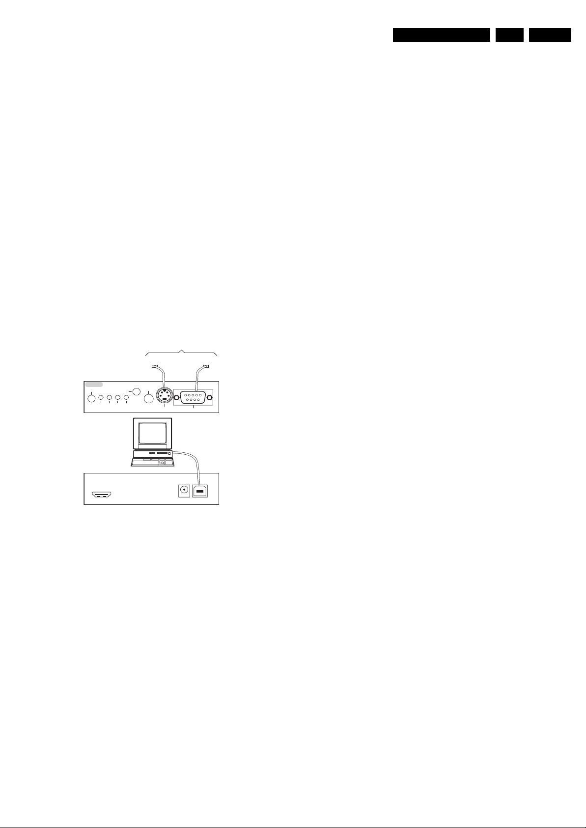
5.1 Service Tools
5.1.1 ComPair
Introduction
ComPair features TV software upgrade possibilities.
Specifications
ComPair consists of a Windows based program and an
interface box between PC and the product. The (new) ComPair
II interface box is connected to the PC via an USB cable. For
the TV chassis, the ComPair interface box and the TV
communicate via a bi-directional cable via the service
connector(s).
How to Connect
This is described in the chassis fault finding database in
ComPair.
TO TV
OR
RS232 /UART
TO
UART SERVICE
CONNECTOR
ComPair II
RC in
Optional
Switch
Power ModeLink/
Activity
RC out
I2C SERVICE
CONNECTOR
Multi
function
TO
2
C
I
Perform measurements under the following conditions:
• Service Default Mode.
• Video: colour bar signal.
• Audio: 3 kHz left, 1 kHz right.
5.3 Service Modes
This chassis does not contain a specific Service Mode. Service
and Alignment of the TV set can be done via the Factory Mode
by the service technician, see further down in this manual.
5.4 Error Codes
Not applicable.
5.5 Fault Finding
5.5.1 Big Snow Dots Visible on the Screen.
Analysis and repair action: according to the problem
phenomena, first check:
(1) Is the antenna signal normal?
(2) Is the tuner and intermediate-frequency circuit power supply
working normally?
(3) Is the AGC circuit of tuner working normally?
(4) Is there a problem with the I2C data stream?
(5) Is there an electricity leak in the circuit layers?
5.5.2 Picture becomes more green after the TV set has been on for more than one hour.
PC
ComPair II Developed by Philips Brugge
Optional power
HDMI
I
2
C only
5V DC
G_06532_036.eps
260107
Figure 5-1 ComPair II interface connection
Caution: It is compulsory to connect the TV to the PC as
shown in the picture above (with the ComPair interface in
between), as the ComPair interface acts as a level shifter. If
one connects the TV directly to the PC (via UART), ICs will be
blown!
How to Order
ComPair II order codes:
• ComPair II interface: 3122 785 91020.
• ComPair32 CD (update): 3122 785 60160.
• ComPair interface cable: 3122 785 90004.
• ComPair interface extension cable: 3139 131 03791.
• ComPair UART interface cable: 3122 785 90630.
• ComPair UART interface cable for Q52x.x
(using 3.5 mm Mini Jack connector): 3104 311 12742.
Note: If you encounter any problems, contact your local
support desk
Analysis and repair action: according to the problem
phenomena, check the following:
(1) Is the antenna signal normal?
(2) If you suspect that there is a heating problem in the channel
circuit, or the circuits after the tuner (colour decoder), use a
blower to reduce the temperature, and check if this has any
effect.
(3) Interrupt and reconnect the antenna signal to find out if the
trouble is in the tuner or the AGC circuit.
(4) Is there a problem with the I2C data stream?
(5) Also check the horizontal deflection pulse.
5.5.3 White Raster Only (no Picture Visible).
Analysis and repair action: if the antenna signal is normal:
according to the problem phenomena, the trouble range can be
divided into six parts: the CPU, the memory chips, the data
transport of the I2C circuit, the horizontal and vertical deflection
pulse circuit, the CRT power supply circuit, and finally the entire
video amplification circuit (including the IF stage). If the CPU or
memory have problems, this will also cause problems of I2C
data. If the problem still cannot be eliminated, check the load of
the I2C lines, namely, the other ICs that are connected to the
I2C bus (they may also have a defect and cause a too heavy
load on the I2C bus. Interrupt the I2C bus to reduce the load
and check again if the CPU puts I2C data on the I2C bus. If the
problem seems to be in the deflection circuits, it may also be
caused by randomly interrupted antenna signals.
5.5.4 The TV set turns ON and OFF randomly when you attempt to turn ON the TV set.
5.2 Test Points
See chapter 6 “Block Diagrams, Testpoint Overviews, and
Waveforms”.
• Check whether the chassis power supply and/or the
horizontal deflection part of the circuit has loose or bad
(corroded) connections, resulting in irregular power supply.

EN 10 SK6.0A CA5.
Service Modes, Error Codes, and Fault Finding
• Check also if the power supply to the CPU is not interrupted
randomly. If the supply voltage is not available or not
normal, change Q602 and Q603.
5.5.5 The TV set is turned ON (indicator light is ON) but no picture and sound is observed.
• Measure the collector voltage of Q303 for 140 V to
eliminate the possibility that the horizontal deflection circuit
is causing the problem. During normal operation, the
collector voltage should be in the range of 110 V.
• Next, measure the horizontal pulse output voltage at Pin 11
of the digital board output terminal. In normal operation, the
voltage is in the range of 2.8 V
the horizontal output transistors Q301 and Q302 are
switching normally between their ON and OFF states.
5.5.6 The TV displays a blue screen when it is turned ON.
The TV set is equipped with a video noise-reduction circuit.
Therefore, when no video and synchronization signal is
detected, the CPU decodes it as “no signal detected”. Check
the antenna signal, the tuner and the IF amplifier circuit.
Replace the Ultimate One Chip of the third generation (UOCIII)
and the peripheral components of the IF circuit, if needed.
5.5.7 Horizontal Deflection Transistor is Defective.
Analysis and repair action: if the deflection time is decreased
too much, this may result in an over-voltage in the deflection
circuit and a defective horizontal transistor. In this case, check
C302, C302A, C303, C304 and C305 for defects.
. If this is correct, check if
AC
5.5.9 Poor picture and sound quality.
• Check if the signal line contact is good.
• Next, use a conductor to touch the IF input of the tuner, if
no effect is observed, the problem is suspected to be in the
IF amplification circuit.
• Use a 0.01 µF capacitance to short the input and output
terminals of SAW101 to isolate if the SAW filter is faulty. If
the picture and sound condition does not improve, check
the AGC circuitry, and replace resistors and capacitors
when needed.
5.5.10 The colour disappears after the TV is turned ON for a while.
• Check if the colour system is selected correctly.
• Replace the 24.576 MHz crystal, if needed.
• If there is no effect, then replace suspected components in
the decoding and colour circuitry.
5.5.11 Soft volume can still be heard, even when volume level is reduced to “0”.
• Check if the peripheral networks connected to pin 122
(MUTE) and pin128 (AV MUTE) of UOCIII are well
connected.
• Proceed to check the audio control and power amplifier
module (IC401); check the surrounding components of
IC401. For example check C407, if it is correctly connected
and shows no leakage. Check whether Q401 switches
normally between its saturation and cut-off states?.
5.5.12 No colour in AV state
5.5.8 In the picture appears a horizontal bright line.
• Check the vertical deflection loop for poor contact.
• Check the vertical IC power supply for +15 V and -15 V.
– If no voltage is present, check R331 for open circuit.
– If the voltage is low, change the vertical deflection IC.
– If the problem still exists, change the surrounding
components in the circuit (e.g. C325, C326 etc.).
• First, check the video input module.
• Second, check the A-D module.
• Next, check the video processor module.
• Finally, check if UOCIII has a defect.
Block Diagrams, Test Point Overviews, and Waveforms
6. Block Diagrams, Test Point Overviews, and Waveforms
Block Diagram Digital Board 100Hz
1
Block Diagram Digital Board 100Hz
2
3
11SK6.0A CA 6.
4
5
6
D
C
TO CRT
PW1235
PW1235.Sch
HS_PW
VS_PW
PW_Rout
PW_Gout
PW_Bout
PW1235_power
PW1235_power.Sch
TDA8380
TDA8380.Sch
PW_Bout
PW_Gout
PW_Rout
VS_PW
HS_PW
Rout
Gout
Bout
AKB
FBlank
R-insert
G-insert
B-insert
ADY[7:0]
ADU[7:0]
ADV[7:0]
GHS
GVS
GCLK
SDA
SCL
RES_PW
SDA
SCL
H_Driver
EW
SVM
EHT
ABL
FBP
Vguard_Vs
V+
V-
TDA8759
TDA8759.sch
ADY[7:0]
ADU[7:0]
ADV[7:0]
GHS
GVS
GCLK
SDA
SCL
UOC_HFB
UOC_VD
UOC_RO
UOC_GO
UOC_BO
IBLK
PD
UOC_III
UOC_III.Sch
PD
IBLK
UOC_BO
UOC_GO
UOC_RO
UOC_VD
UOC_HFB
SCL
SDA
RES_PW
VIS
HIS
OSD_Ready
OSD_RESET
VIS
HIS(OSD)
YPbPr_Y
YPbPr_Pb
YPbPr_Pr
VGA_R
VGA_G
VGA_B
VGA_HS
VGA_VS
SDA1
SCL1
LED
Key1
Key2
Stand_by
H_fre1
H_Prote
Tilt
D
Interfa ce
Interfa ce.Sch
YPbPr_Pr
YPbPr_Y
YPbPr_Pb
VGA_B
VGA_G
VGA_R
USE FOR TUNER
AND SOFTWARE UPDATE
C
IR
TO FORNT KEY
TO MAIN BOARD
SR
Mute
L_out
R_out
YCbCr_Y
YCbCr_Cb
YCbCr_Cr
AGC
BUS_off
SCL2
SDA2
WP
Vo
Lo
Ro
IF
USE FOR E2PROM
H_17230_029.eps
B
A
070807
FBL2
B
OSD
OSD.sch
B-insert
G-insert
R-insert
FBlank
HIS(OSD)
NO USE
A
1234 65
SVM_SW
HIS
OSD_Ready
OSD_RESET
SDA
SCL
Vguard_Vs
FBP
NO USE
AV_Mute
L3
R3
C1
Y1
V2/Y2
C2
L2
R2
V1
L1
R1
Block Diagrams, Test Point Overviews, and Waveforms
Block Diagram Chassis (Digital Board 100Hz)
12SK6.0A CA 6.
Block Diagram Chassis (Digital Board 100Hz)
CVI YCAV SIDE
D
Y
A4
5V
33V
C
TUNER SDA
EEPROM
24C16
C3
OSD
M37161
Cb
Cr
IF
SCL
SDA2
SCL2
RESET
HIS
SDA
SCL
R
G
B
CVBS
7654321
AV OUT
Y
L
R
C
CVBSLR
CVBSLR
Y
YPbPr
Pb
Pr
8
D
G
A5
C4
UOC3
TDA12063
SDA
SCL
R
G
B
VS
HS
VIS
SDA
SCL
VGUARD
C5
ADC
TDA8957
SDA
SCL
RESET
C1
DISPLAY
OM8380
ADY[0-7]
ADU[0-7]
ADV[0-7]
VS
HS
CLK
R
G
B
VS
HS
C2
SCALER
PW1233
C
B
M
A
6P19/6P19S block diagram
12345678
TO SPEAKER
EW-PCB
(SLIM ONLY)
A6
TDA7266SA
AUDIO AMP
A2
H-SCAN
POWER
HS
L
R
MUTE
HOUT
EW
FBP
A3
V-SCAN
VP
VN
VGUARD
VDY-P
VDY-N
HDY-P
HDY-N
EHT
SCREEN
FOCUS1
FOCUS2
ROTARY
SVM
ROTARY
SVM
ROTARY
SVM
CRT
B
CRT PCB
RGB
RGB
AKB
+13.5V(AUDIO-AMP)
A1
POWER
STR-W6756
AC160-260V 50/60Hz
+8V(ADC,SCALER)
+141V(FLYBACK,TUNER)
+13.5V(UOC3,OM8380,M37161)
B
E
A
H_17230_030.eps
290607
Block Diagrams, Test Point Overviews, and Waveforms
Schematic Diagram Chassis (Overview)
321
13SK6.0A CA 6.
4
5
6
7
8
11109
12
C211 0.033uF
C210 0.047uF
2
R203
1
100
CON2
C2130.1uF
D
630V
D210 BA158
C230 0.001uF
R212
R213
100K
100K
EW PCB(for slim)
C
R0
R428
240K/1/6W
L0
R427
V0
240K/1/6W
GND
Pr
R436
Y
Pb
GND
B
Mains Filter
A
CN601
SW601
!
AC220V
!
1
630V
630V
C2140.056uF
R435
75/1/6W
8.2V
R437
75/1/6W
630V
75/1/6W
C201
0.1uF
630V
R224
47
2KV
R214
150K
C429
100pF/50V
C428
100pF/50V
R441
75/1/6W
D430
T3.15A 250V
R601
C209
1000pF
R215
150K
C421
10uF/16V
C420
10uF/16V
GND
Pr
Y
Pb
GND
2.2M 1/2W
500V
ZD201
R202
12V
100K 2W
C202
4.7uF
250V
D220
BA158
3K9
R232 5K1 R211
C422
470uF/16V
R442
470K/1/6W
H403
1
2
3
4
R1
1
2
3
4
5
6
7
8
9
CON400
Y1
!
F601
VDR601
CMQX0680-3C 680V
C613
1000p/2KV
R611
0.82/2W
TH605
!
V209
F630
C212
100uF
25V
D221
BA158
R230 13K
R2372KR236
8K2
C203
1.0uF
100V
1K
D420
8.2V
GND
R2
L2
V2
L1
V1
C1
0.47uF/AC250V
L602
!
15mH
!
C601
0.47uF/AC250V
RST601
GIGA SURGE ABSORBER 30 0V
220/1W
1
IC601
D
STR-W6756
S/GND
3
C615
220p/500V
R613
0.18/2W
R612
100/1W
1
C215 0.012uF
630V
C200 0.1uF
R205
47
C424
100pF/50V
GND
C423
100pF/50V
GND
C602
32
R424
75/1/6W
R426
75/1/6W
R425
75/1/6W
GND
!
GST601
OLP/SS
D209 14148
R217 270K
R216 22K
Cr
Cb
Y
R431
240K/1/6W
R432 240K/1/6W
R434
75/1/6W
L601
15mH
!
4
VCC
FB
OCP/BD
7
C617
470PFAC400V
R220
100K
R239 2K4
R238 7K5R231
V207
C1815
GND
R422
240K/1/6W
R421
240K/1/6W
GND
6
5
!
V203
C1815
C431
100pF/50V
C432
100pF/50V
L603 (R602)
!
C603
0.22uF/AC250V
C614
1uF/50V
R610
18K
1
R440
75/1/6W
R438
75/1/6W
R439
75/1/6W
D604
EU1Z
D424
8.2V
28mH˄
D202
14148
R207
100
R218
100K
R423
39K/1/6W
R420
39K/1/6W
4/15W
BR605
KBJ6J
C618
470PFAV400V
R604
68K/ 2W
ZD601
6V2
R608
1K/1/4W
C612
0.1uF/50V
32
!
R221
22K
R219
3K9
C607
4n7/2KV
ZD602
16V
CN602
˅
TH603
4n7/2KV
C605
!
V0L0R0
D432
8.2V
R430
39K/1/6W
R429
39K/1/6W
R433
220/1/6W
!
R206
4K7
CrCbY2
R600
5
C608
D207
14148
R208
1K
C609
220uF/450V
R607 1K/1/4W
D605
BA158
C611
10uF/63V
C616
0.0015uF/50V
D606
BA158
0.1uF/250~500V
H602
V204
C1815
D206
14148
C207
10uF
50V
H_17230_031a.eps
R209
470K
C208 0.1uF
R233 5K1
R210
100K 1/2W
C109
0.001uF/50V
Part 1
630V
C108
100uF/16V
IC603
PC817
!
L0R0V0
SCL1
SDA1
L0
R0
V0
GND
L1
R1
Y1
V1
C1
IF
GND
AGC
3V3
SDA1
SCL1
WP
SDA2
SCL2
GND
R104
100/1/6W
R103
100/1/6W
!
IF
AGC
GND
T601
*
C610
0.01uF/1KV
9
R605
100K/2W
D602
1N5397
D602A
6
C610A
680pF/1KV
1N5397
FB601
R606
10/1/4W
2
D603
EU1Z
R609
1K/1W
3
BCK4222
!
C619
0.0022uF
R626
8.2M/1W
!
!
630V
C216
R204
100
1000pF
1
Cb
2
Y
3
4
Cr
5
6
7
8
9
10
11
12
13
14
15
16
17
18
20
19
21
22
24
23
26
25
28
27
30
29
32
31
34
33
36
35
38
37
40
39
IC002
1
3.3V
GND
2
WP
GND
3
SCL2
GND
4
SDA2
GND
ST24C16
R627
1K/1/6W
R643
10K/1/6W
C660
0.1uF/63V
GND
16
140V
FB623
C635
680pF/2KV
18
GND
FB622
14
12V
C632
15
220pF/500V
GND GND
10
7V5
R623
FB621
0.22
C628
11
220pF/500V
GND
12
13V
R624
FB620
0.22
13
CbYCr
L1
R1
Y1
V1
L2
R2
V2
+5V_U
GND
GND
Hs
Vs
Wp
SDA2
SCL2
GND
D626
LG16S
0.01uF/500V
D625
RG2Y
D624 RG2Y
D623
RU4YX
C624
680pF/500V
SDA2
+5V_U
SCL2
8
7
6
5
GND
R629
1K/1/6W
GND
D627
BA158
C637
C638
220uF/160V
C634
3300uF/16V
C633
220pF/500V
GND
C630
1000uF/16V
C627
2200uF/16V
C625
D622
RU4YX
1000uF/25V
Part 3
V208
F630
C640
100uF/50V
R642
C631
0.01uF/50V
0.01uF/50V
+5V_D
+5V_CPU
P_chk
HOUT
FBP
+8V
MUTE
LOUT
ROUT
EHT
ABL
H_PRO
100K/1/2W
C636
0.01uF/50V
R633
1R5/2W
C629
0.01uF/50V
C626
R229
47
GND
GND
GND
H_17230_031c.eps
234
R113
100K/1/6W
AGC
D628
C639
C206
10uF
50V
D204
D203
14148
R228
100
V206
C1815
AGC1GND2AS3SCL
TUNER
DGND
CGND
GND
GND
GND
GND
GND
BA158
R631
120/2W
R628
100K/1/2W
10uF/160V
GND
R112
6K8/1/6W
120/2W
R631A
R618
5R1/2W
C653
0.33uF/63V
R619
0.33/2W
GND
1
3
5
7
9
11
13
15
17
19
21 22
23
25
27
29
VS
31
33
35
37
39
Q603
A1930
R640 56/2W
IC607
123
L7808
GND
GND
R111
10k/1/6W
C107
4.7uF/16V
R635
3K3/1/6W
R637 33/2W
IC605
123
L7805
R644
10K/1/6W
2K7/1/2W
Q604
A1015
R622
GND C105
Stand-By
2
4
6
8
10
12
14
16
18
20
24
26
28
30
32
34
36
38
40
ZD620
5V1
D630
BA158
GND
R625
2R7/2W
C654
1000uF/16V
C649
330uF/16V
GND
C644
470uF/16V
0.01uF/50V
GND
R107 100/1/6W
STY
SVM
TILT
CGND
P_chk
HOUT
FBP
GND
+8V
GND
+5V_A
E/W
GND
V-
V+
VS
GND
C411
R227
4K7
SCL1
SCL1
Q602
C2230
C648
0.01uF/50V
R641
C645
0.1uF/50V
SDA
5
R108 100/1/6W
SDA1
SDA1
IC602
SE130
R634
22k/1/6W
GND
51/2W
GND
R645
330K/1/6W
GND
V205
C1815
+5V7GND8+33V9IFGND10IF
6
47uF/16V
C106
0.01uF/50V
C102
22uF/50V
R110
27/1W
GND
+8V
R106 100/1/6W
R105 100/1/6W
V-V+VS
E/W
1
2
3
GND
R636 180/2W
IC604
123
L7805
GND
IC608
123
L7805
R638 22/2W
IC606
123
L7805
GND
D631
1N4148
C652
100uF/16V
C641
1000uF/25V
GND
GND
ZD101
5V1
GND
C103
0.01uF/50V
5V_A
R641A
51/2W
GND
SVM
R630
3.9K/1/6W
C651
470uF/16V
+33V
R301
10K/2W
C642
1000uF/16V
0.1uF/50V
C646
470uF/16V
GND
IC003
KA33
SDA2
+15V
+13V(SOUND)
Stand-by(from UOC)
C643
C650
0.1uF/50V
C647
0.1uF/50V
J301
SCL2
8.2K/2W
14148
11
C101
0.01uF/50V
IF
R101
100/1/6W
R102
100/1/6W
+33V
+140V
+5V_CPU
+8V
+5V_U
+13V
+5V_D
5V_A
P_CHK
5V-CPU
+13V(SOUND)
D205
14148
C205 0.1uF
630V
R223 82K
1W
R222
270
+5V
CN100
123
123
GND
*2 x 6W
LOUT
ROUT
+5V_CPU
MUTE
5V_D
+15V
E/W
Vs
+5V_CPU
V+
V-
+15V
+8V
FBP
+13V
HOUT
R409A
GND
10K/1/6W
R410A
10K/1/6W
100/1/6W
J325
100/1/6W
J324
GND
D629
1N4148
D301
BA158
R304
180/1/2W
C310
10uF/50V
Q301
GND
C1815
C315
R306
4.7uF/50-100V
68/1/6W
R305
100
D307
IN4148
4
4
R302A
5R6/2W
GND
R225
470K
R234
5K1
R235
5K1
R409
10K/1/6W
R327A
15/2W
C309
0.001uF/50V
C313
0.001uF/500V
3K3/1/6W
C314
22nF/100V
R309
10K/1/6W
IC401
TDA7266
10K/1/6W
R330
1K8/1/6W
R302
5R6/2W
CRT AMPLIFY CIRCUIT
R226
1K
H501
IN212VCC13OUT2-14OUT2+
15
R403
8R2/1/6W
R408
GND
R308
47/2W
0.22uF/63V
NC
11
C403
4n7/100V
GND
C404
0.01uF/50V
C405
R410
C406
0.22uF/63V
R411
22K/1/6W
IC301
TDA4863AJ
R329
1K8/1/6W
R322
C328
5.6/1/6W
0.1uF/63V
R324
R327
220/2W
0.68/2W
R327B
10
D302
BA158
R310
GND
0.51/2W
T301
H-DRIVER
R341
Q302
12/1/4W
C2026
GND
C501
100uF
50V
GND
R505
33
R508
33
R
GND
G
GND
B
GND
33
10
GND
GND
R404
47K/1/6W
C402
4n7/100V
C408
4.7uF/16V
C327
0.1uF/100V
ZD301
7V5
D306
BYW36
GND
Q303
5859
GND
R328
5R6/1/6W
C302A
GND
1n/2KV
J401
100/1/6W
100uF/16V
GND
1n/2KV
C407
100/1/6W
R406
2K/1/6W
Q401
C1815
R303
12K/2W
56pF/500V
C301
D303
1N4148
+140V
J403
ZD401
4.3V
C325
100uF/50V
R342
220/2W
C332
1000uF/25V
C302
R511
C410
D305
BY459
FB301
D304
211060
H-PRO
330uF/25v
C333
0.01uF/50V
GND
C312
470pF/2KV
C311
0.0047UF/500V
C303
*8n2/2KV
D311
IN4148
IR
R405 47K/1/6W
D401
BA158
GND
GND
INP7INN6V-OUT5GND4VP23VP32VP1
R523
6.2K
Q502
2SC1815Y
R527
510
R516
6.2K
Q506
2SC1815Y
R521
510
R513
6.2K
Q510
2SC1815Y
R517
510
GND
C335
1000uF/25V
GND
R319
1K/1/6W
R531
470
R526
220
R536
470
R522
220
R539
470
R518
220
Q304
C1815
C319
22uF/250V
R528
150
R533
150
R538
150
D308
BA158
GND
-15V
R307 1.7/5W
D315
RG2Y
+15V
C336
680pF/500V
R506
22
Q503
2SA1015
R529
220
R556
100/1/6W
R509
22
Q507
2SA1015
R534
220
R512
22
Q511
2SA1015
R541
220
680pF/500V
C316
100uF/200V
C331
680pF/500V
C502
R504
0.01uF/50V
22
C503
22uF/50V
Q501
GND
2SC1815Y
R524
470
L501
LPF16M
R525
1.5K
GND GND GND GND GND
C504
R507
0.01uF/50V
22
C505
22uF/50V
GND
Q505
2SC1815Y
R519
L502
470
LPF16M
R520
1.5K
GND GND GND GND GND
C506
R510
0.01uF/50V
22
C507
22uF/50V
Q509
GND
2SC1815Y
R514
470
L503
LPF16M
R515
1.5K
GND GND GND GND GND
OUT-
VCC3IN14NC5MUTE6ST-BY7PW-GND8S-GND9NC
OUT1+
2
1
R401
R402
10/1/6W
82K/1/6W
R407
GND
GND
D314
BA158
C305
*18n/630V
+5V_CPU
47K/1/6W
C409
22uF/16V
*3n3/2KV
1
C324
0.33uF/63V
R331
0.68/2W
C304
C323
1uF/50V
C401
0.01uF/50V
L-L+R-
R+
H401
C326
1000uF/25V
GND
R340
22K/1/6W
R318
22K/1/6W
D312
IN4148
GND
GND
CN302
+15V
+140V
+200V
HEAT
GND
GND
R320
10K/1/6W
C334
R321
0.01uF/50V
10K/1/6W
GND
R348
N.C
R339
100/1/6W
R311
0.68/2W
C318
R316
D316
RG2Y
3.9K/1/6W
0.68/2W
R326
CN301 H
10
GND
R315
0.22/2W
R532
1K/1/6W
R530
FB
R537
1K/1/6W
R535FBR544
R540
1K/1/6W
R542
FB
J381
100/1/6W
8V
ZD302
8V2
GND
V
T302
1
2
9
8
6
4
5
Q504
2SA1015
Q508
2SA1015
Q512
2SA1015
IC502
TDA6111Q
D501
1N4004
GND
R551
C543
2.7K
GND
C527
GND
C542
100uF/25V
GND
GND
R552
2.7K
C536
GND
GND
R550
C522
2.7K
GND
0.01uF/50V
R546
0.01uF/50V
0.01uF/50V
R548
C510
22uF/50V
C509
2K
C51910pF
C512
22uF/50V
C511
2K
C51710pF
C514
22uF/50V
C513
2K
C52110pF
H_17230_031b.eps
C381
100uF/25V
R381
1K8/1/6W
R380
1K/1/6W
GND
R383
1K/1/6W
Q380
C1815
C380
1uF/50V
R382
10K/1/6W
GND
R384
470/1/6W
Q385
C1815
C382
1uF/50V
GND
GND
R325
R323
68K/1/4W
2R2/2W
Q305
F6300
12
13
7
C339
0.1uF/250V
C330
0.01uF/50V
1
2
connect to CON2
EHT
FOCUS
G2
R312
GND
D310
2K/1/4W
BA158
R313
2K/1/4W
GND
C320
N.C
GND
L302
*3.5uH
C329
0.001uF/50V
R317
270/1W
C322
0.001uF/1KV
*
!
VDDL2VIP 1VIN3GND4IOM5VDDH6VCN7VOC8VPB
C534
C528
0.01uF/50V
0.1uF/50V
GND GND
IC503
TDA6111Q
VDDL2VIP 1VIN3GND4IOM5VDDH6VCN7VOC8VPB
C540
C537
0.01uF/50V
0.1uF/50V
GNDGND
IC501
TDA6111Q
VDDL2VIP 1VIN3GND4IOM5VDDH6VCN7VOC8VPB
R549A
C525
0.01uF/50V
C523
GND GNDGND
Part 2
C383
0.22uF/63V
Q381
C1815
Q382
A1015
GND
Q384
C1815
Q383
A1015
GND
C308
4.7uF/50V
L301
*130uH
D309
4.7K/1/6W
2.7K/1/6W
R333
9.1K/1/4W
+15V
R573
C541
R567
220K/1W
2SA1480
C532
0.22uF/250V
1.5/2W
0
C515
0.0022uF/2KV
Q706
2SA1837
R717
68K
R711
22
R709
+15V
G1
GND
+15V
GND
10
Q701
2SC1815Y
D505 BA159
GND
C531 10uF/250V
R563
4.7M/1/4W
GND
+140V
C711
10uF/250V
R710
22
D701
IN4148
R704
150
GND
R572
100/2W
C508
22uF/250V
D502
BA158
+200VNCHEAT
CN702
D704
IN4148
C706
0.0047uF/500V
R723
270/2W
+140V
150/1W
ZD501
12V
R572A 0.18/ 2W
R562
56K/1/4W
R561
1.5K//1/2W
C530
2200pF/2KV
CN502
EHT
FOCUS
G2
R722
2.7/1/2W
GND
Q704
2SC1815Y
Q703
2SC1815Y
GND
D
*
CRT
!
GND
GND
C
R721
56/1W
C709
100uF/16V
R720
1.2K
C704
100pF/50V
Q702
2SC1815Y
R706
68
GND
R705
1K
C703
47uF/25V
R719
1.5K
C710
10uF/250V
GND
B
A
Q513
2SA1015
R565
5.6k
9
R554
C533
560pF/500V
220K/1W
R564
R558
R554A
1K/1/2W
R555
10/1/6W
C535
0.22uF/250V
220K
GND
9
C538
560pF/500V
R560
220K/1W
R560A
R559
220K
GND
220K
0.1uF/50V
CN380
R337
1K/1/2W
GND
L506
R556A 10/1/6W
C539
15uH
0.22uF/250V
9
R549
C524
220K/1W
560pF/500V
R557
1K/1/2W
R553
10/1/6W
GND
C526
0.22uF/250V
Q707
2SC4793
R712
C708
1.5K
R714
100uF/50V
56/1W
R715
R713
2.7/1/2W
1.2K
D703
GND
IN4148
GND
C702
2.2uF/50V
C337
N.C
R351
1M/1/2W
GND
R338
100K/1/6W
GND
EHT
R336
22K/1/6W
D313
IN4148
ABL
2.2K/1/6W
GND
R570
18K
R569
10K/1/6W
C529 22uF/250V
L505
15uH
L504
15uH
L702 L703
R716
68K
C707
0.0047uF/100V
C705
100pF/50V
Q705
2SA1015Y
R707
1K
R708
33K
R701
3.3K
R702
18K
C701
3pF/50V
100uF/25V
R566
22K
GND
D506
IN4148
Q514
R568
220K
BA159
D504
!
G501
*
GND
R571
R571A
GND
H502
R724
220/2W
L701
R718
12K
D702
IN4148
R703
470/1W
GND
SVM
Part 4
H_17230_031d.eps
5
678910 21
11
H_17230_031.eps
290607
Block Diagrams, Test Point Overviews, and Waveforms
W
Schematic Diagram Chassis (Part 1)
14SK6.0A CA 6.
GND
SCL2
6
11
C101
0.01uF/50V
IF
D204
14148
C206
10uF
50V
D205
14148
C205 0.1uF
R223 82K
R222
270
+5V
CN100
1
2
630V
1W
R225
470K
R234
5K1
R235
5K1
3
4
C216
1000pF
CbYCr
4
V208
F630
R229
47
TUNER
R112
6K8/1/6W
R113
100K/1/6W
AGC
321
C211 0.033uF
630V
C210 0.047uF
630V
C2140.056uF
630V
2KV
R224
47
R214
150K
C201
0.1uF
630V
C209
1000pF
R202
100K 2W
R215
150K
500V
C202
4.7uF
250V
3K9
2
1
CON2
D
R213
100K
R203
100
C2130.1uF
630V
D210 BA158
C230 0.001uF
R212
100K
ZD201
12V
D220
BA158
V209
F630
R230 13 K
R236
8K2
C203
1.0uF
100V
R205
47
C212
100uF
25V
D221
BA158
R237
2K
V203
C1815
R220
100K
D209 14148
R239 2K4
R238 7K5R231
V207
C1815
R217 270K
R216 22 K
R218
100K
D202
14148
R207
100
R0
R221
22K
R219
3K9
V204
C1815
R206
4K7
D206
14148
C207
D207
10uF
14148
50V
R209
R208
1K
470K
C208 0.1uF
R233 5K1
CrCbY2
V0
L0
630V
R210
100K 1/2W
IF
AGC
V0
SCL1
SDA1
C215 0.012uF
630V
C200 0.1uF
630V
R204
100
Part 1
L0
R0
5
D203
14148
R228
100
V206
C1815
AGC1GND2AS3SCL
GND
GND
R111
10k/1/6W
C107
4.7uF/16V
GND
V205
C1815
R227
4K7
SDA
5
R107 100/1/6W
R108 100/1/6W
SCL1
SDA1
Stand-By
SDA1
SCL1
+5V7GND8+33V9IFGND10IF
6
C105
47uF/16V
R110
+8V
0.01uF/50V
C102
22uF/50V
27/1W
GND
GND
ZD101
5V1
C106
GND
C103
0.01uF/50V
+33V
IC003
KA33
SDA2
EW PCB(for slim)
C
R0
R428
240K/1/6W
L0
R427
V0
Pr
Y
GND
240K/1/6W
R436
R435
75/1/6W
8.2V
75/1/6W
C429
100pF/50V
C428
100pF/50V
R441
75/1/6W
D430
C421
10uF/16V
C420
10uF/16V
R442
470K/1/6W
GND
Pr
Y
Pb
GND
R232 5K1
H403
C422
470uF/16V
1
2
3
4
GND
R211
1K
D420
8.2V
R106 100/1/6W
1
2
3
R105 100/1/6W
L0
1
R0
3
V0
5
7
GND
L1
9
R1
11
Y1
13
15
V1
C1
GND
GND
IF
AGC
3V3
SDA1
SCL1
WP
SDA2
SCL2
17
19
21
23
25
27
29
31
33
35
37
39
R440
GND
C431
100pF/50V
C432
100pF/50V
75/1/6W
R438
75/1/6W
R439
75/1/6W
D432
8.2V
R430
39K/1/6W
R429
39K/1/6W
Cr
Cb
Y
R431
240K/1/6W
R2
L2
R432 240K/1/6W
Cb
2
Y
4
Cr
6
8
10
L1
R1
12
Y1
14
V1
16
18
L2
20
R2
22
V2
+5V_U
24
26
GND
28
GND
Hs
30
Vs
32
34
Wp
SDA2
36
SCL2
38
40
GND
SDA2
+5V_U
+5V_D
+5V_CPU
P_chk
HOUT
FBP
+8V
MUTE
LOUT
ROUT
EHT
ABL
H_PRO
DGND
CGND
GND
GND
GND
GND
GND
1
3
5
7
9
11
13
15
17
19
21 22
23
25
27
29
VS
31
33
35
37
39
2
STY
4
SVM
6
TILT
8
CGND
10
P_chk
12
HOUT
FBP
14
16
GND
18
+8V
20
GND
+5V_A
24
E/W
26
GND
28
V-
30
V+
VS
32
34
GND
36
38
40
UND)
R101
100/1/6W
R102
100/1/6W
H_17230_031a.eps
290607
*2 x 6
4
GND
Block Diagrams, Test Point Overviews, and Waveforms
Schematic Diagram Chassis (Part 2)
15SK6.0A CA 6.
C206
10uF
50V
D205
14148
C205 0 .1uF
R223 82K
R222
270
+5V
CN100
1
2
1
2
630V
1W
3
3
GND
7
8
CRT AMPLIFY CIRCUIT
IC502
C527
C536
C522
D501
1N4004
C543
TDA6111Q
GND
VDDL
VIP 1VIN3GND4IOM5VDDH6VCN7VOC8VPB
2
C533
560pF/500V
R554A
R555
220K
220K
R560A
220K
GND
10/1/6W
C535
GND
C538
560pF/500V
GND
R556A 10/1/6W
C539
0.22uF/250V
C524
560pF/500V
R553
10/1/6W
GND
C526
0.22uF/250V
C534
C528
0.01uF/50V
0.1uF/50V
GND GND
IC503
TDA6111Q
VDDL
VIP 1VIN3GND4IOM5VDDH6VCN7VOC8VPB
2
C540
C537
0.01uF/50V
0.1uF/50V
GND GND
IC501
TDA6111Q
VDDL
VIP 1VIN3GND4IOM5VDDH6VCN7VOC8VPB
2
R549A
C525
0.01uF/50V
C523
GND GNDGND
0.1uF/50V
0.22uF/250V
R559
R558
1K/1/2W
R557
1K/1/2W
R531
470
R526
220
R536
470
R522
220
R539
470
R518
220
R528
150
R533
150
R538
150
R506
22
Q503
2SA1015
R529
220
R556
100/1/6W
R509
22
Q507
2SA1015
R534
220
R512
22
Q511
2SA1015
R541
220
R532
1K/1/6W
R530
FB
R537
1K/1/6W
R535
FB
R540
1K/1/6W
R542
FB
C502
R504
0.01uF/50V
22
C503
22uF/50V
Q501
GND
2SC1815Y
R524
470
L50 1
LPF1 6M
R525
1.5K
GND GND GND GND GND
C504
R507
0.01uF/50V
22
C505
22uF/50V
Q505
GND
2SC1815Y
R519
L50 2
470
LPF1 6M
R520
1.5K
GND GND GND GND GND
C506
R510
0.01uF/50V
22
C507
22uF/50V
Q509
GND
2SC1815Y
R514
470
L50 3
LPF1 6M
R515
1.5K
GND GND GND GND GND
R523
6.2K
Q502
2SC1815Y
R527
510
R516
6.2K
Q506
2SC1815Y
R521
510
R513
6.2K
Q510
2SC1815Y
R517
510
GND
R505
33
R508
33
33
C501
100uF
50V
R511
R226
R225
470K
1K
R234
5K1
R235
5K1
H501
R
4
4
GND
G
GND
B
GND
IR
GND
Q504
2SA1015
Q508
2SA1015
Q512
2SA1015
C510
0.01uF/50V
R546
10pF
0.01uF/50V
R544
0.01uF/50V
R548
22uF/50V
C509
2K
C519
22uF/50V
C511
2K
C51710pF
22uF/50V
C513
2K
C52110pF
C512
C514
GND
GND
GND
GND
GND
GND
GND
R551
2.7K
C542
100uF/25V
R552
2.7K
R550
2.7K
11109
Q513
2SA1015
R565
5.6k
9
R566
R554
220K/1W
R564
9
R560
220K/1W
1K/1/2W
L50 6
15uH
L50 4
9
15uH
R549
220K/1W
22K
2.2K/1/6W
GND
R570
18K
R569
R568
220K
10K/1/6W
C529 22uF/250V
L50 5
15uH
D506
IN4148
GND
G501
R571A
H502
Q514
BA159
D504
!
*
R571
GND
C541
100uF/25V
R567
220K/1W
2SA1480
C532
0.22uF/250V
GND
1.5/2W
0
GND
C515
0.0022uF/2KV
+15V
GND
C531 10uF/250V
R563
4.7M/1/4W
D502
BA158
D505 BA159
GND
G1
+140V
+200VNCHEAT
GND
R572
100/2W
C508
22uF/250V
ZD501
12V
EHT
FOCUS
R573
150/1W
R572A 0.18/ 2W
R562
56K/1/4W
R561
1.5K//1/2W
C530
2200pF/2KV
CN502
CRT
!
G2
GND
GND
12
D
*
a.eps
0607
*2 x 6W
IC401
TDA7266
15
R403
8R2/1/6W
C
Part 2
H_17230_031b.eps
290607
C381
OUT2-14OUT2+
IN212VCC
13
NC
NC
10
11
GND
R405 47K/1/6W
D401
BA158
PW-GND
S-GND
8
9
J401
100/1/6W
C407
100uF/16V
MUTE
ST-BY
6
7
IN1
4NC5
R401
82K/1/6W
/1/6W
R407
OUT-
VCC
3
OUT1+
2
1
R402
10/1/6W
100uF/25V
GND
R383
1K/1/6W
R381
1K8/1/6W
R380
1K/1/6W
Q380
C1815
C380
Q381
C1815
Q382
C383
0.22uF/63V
CN380
Block Diagrams, Test Point Overviews, and Waveforms
9
F
K/
75/1/6W
H403
2
2
Schematic Diagram Chassis (Part 3)
B
A
Pr
8.2V
R436
Y
Pb
GND
AC220V
75/1/6W
R437
75/1/6W
Mains Filter
CN601
SW601
!
!
D430
T3.15A 250V
R601
2.2M 1/2W
GND
Pr
1
Y
2
Pb
3
4
1
2
3
4
5
6
7
8
9
CON400
!
F601
VDR601
C613
1000p/2KV
R2
L2
V2
R1
L1
V1
C1
Y1
0.47uF/AC250V
L60 2
!
15mH
!
C601
0.47uF/AC250V
CMQX0680-3C 680V
RST601
GIGA SURGE ABSORBER 300V
220/1W
1
D
C424
100pF/50V
C602
IC601
STR-W6756
S/GND
3
C615
220p/500V
R613
R611
TH605
0.18/2W
0.82/2W
R612
100/1W
!
1
GND
GND
C423
100pF/50V
R424
75/1/6W
R426
75/1/6W
R425
75/1/6W
GND
GST601
32
R432 240K/1/6W
R434
75/1/6W
!
L601
15mH
!
4
VCC
FB
OLP/SS
OCP/BD
7
C617
470PFAC400V
GND
6
5
!
C431
100pF/50V
C432
100pF/50V
D424
R422
240K/1/6W
R421
240K/1/6W
28m H
L603 (R602)
!
C603
0.22uF/AC250V
C614
1uF/50V
D604
EU1Z
R610
18K
1
8.2V
R423
39K/1/6W
R420
39K/1/6W
˄
BR605
KBJ6 J
470PFAV400V
4/15W
R604
68K/ 2W
ZD601
6V2
R608
1K/1/4W
C612
0.1uF/50V
32
!
C618
˅
4n7/2KV
C605
C607
4n7/2KV
ZD602
16V
TH603
CN602
R430
39K/1/6W
R429
39K/1/6W
R433
220/1/6W
!
!
R600
5
C608
C609
220uF/450V
R607 1K/1/4W
D605
BA158
C611
10uF/63V
C616
0.0015uF/50V
D606
BA158
0.1uF/250~500V
!
H602
C610
0.01uF/1KV
C610A
680pF/1KV
FB601
R606
10/1/4W
D603
EU1Z
R609
1K/1W
1N5397
D602A
C109
0.001uF/50V
9
R605
D602
1N5397
6
2
3
GND
T601
100K/2W
BCK4222
C108
100uF/16V
IC603
PC817
!
C619
16SK6.0A CA 6.
EHT
ABL
H_PRO
SDA2
+5V_U
SCL2
R104
100/1/6W
IC002
1
3.3V
R103
100/1/6W
2
WP
3
SCL2
4
SDA2
ST24C16
!
R627
1K/1/6W
R643
10K/1/6W
C660
0.1uF/63V
GND
16
140V
*
!
0.0022uF
R626
8.2M/1W
!
FB623
C635
680pF/2KV
18
GND
FB622
14
12V
C632
15
220pF/500V
GND GND
10
7V5
R623
FB621
0.22
C628
11
220pF/500V
GND
12
13V
FB620
13
GND
GND
GND
GND
D626
LG16 S
0.01uF/500V
D624 RG2Y
D623
RU4YX
C624
680pF/500V
R624
0.22
8
7
6
5
GND
R629
1K/1/6W
D625
RG2Y
C633
220pF/500V
D622
RU4YX
C637
D627
BA158
220uF/160V
C634
3300uF/16V
GND
C630
1000uF/16V
C627
2200uF/16V
C625
1000uF/25V
GND
C638
C631
0.01uF/50V
0.01uF/50V
C640
100uF/50V
R642
100K/1/2W
C636
0.01uF/50V
R633
1R5/2W
C629
0.01uF/50V
C626
GND
D628
GND
GND
IC602
SE130
R635
3K3/1/6W
C649
330uF/16V
GND
Q604
A1015
R622
ZD620
5V1
D630
BA158
GND
R625
2R7/2W
C654
1000uF/16V
C644
470uF/16V
0.01uF/50V
GND
Q602
C2230
C648
0.01uF/50V
R641
C645
0.1uF/50V
C411
GND
R634
22k/1/6W
GND
51/2W
GND
R645
330K/1/6W
BA158
Q603
A1930
R631
120/2W
120/2W
R631A
R628
100K/1/2W
C639
10uF/160V
GND
R640 56/2W
IC607
123
L7808
R637 33/2W
IC605
123
R619
0.33/2W
L7805
R644
10K/1/6W
GND
2K7/1/2W
R618
5R1/2W
C653
0.33uF/63V
V+
VS
E/W
1
2
3
GND
R636 180/2W
IC604
123
L7805
GND
IC608
123
L7805
R638 22/ 2W
IC606
123
L7805
GND
D631
1N4148
C652
100uF/16V
C641
1000uF/25V
GND
V-
5V_A
R641A
51/2W
GND
SVM
R630
3.9K/1/6W
R301
10K/2W
C642
1000uF/16V
0.1uF/50V
C651
470uF/16V
C646
470uF/16V
+15V
+13V(SOUND)
Stand-by(from UOC)
J301
8.2K/2W
C643
C650
0.1uF/50V
C647
0.1uF/50V
+13V(SOUND)
+33V
+140V
+5V_CPU
+8V
+5V_U
+13V
+5V_D
5V_A
P_CHK
5V-CPU
LOUT
ROUT
+5V_CPU
MUTE
5V_D
+15V
E/W
Vs
+5V_CPU
V+
V-
+15V
+8V
FBP
+13V
HOUT
J325
J324
R304
180/1/2W
Q301
C1815
R306
68/1/6W
R305
100
GND
R410A
100/1/6W
100/1/6W
D301
BA158
C310
10uF/50V
C315
4.7uF/50-100V
R409A
10K/1/6W
10K/1/6W
GND
D629
1N4148
GND
D307
IN4148
10
R302A
5R6/2W
C30
0.00
C313
0.001u
GND
R4
R3
15/
Part 3
H_17230_031c.eps
290607
1
234
5
6
HOUT
100uF/25V
U
C
C
U
W
G
C
C
2
C
U
U
U
Block Diagrams, Test Point Overviews, and Waveforms
Schematic Diagram Chassis (Part 4)
V
O
OUT
OUT
V_CPU
UTE
V_D
15V
/W
s
5V_CPU
V+
V-
5V
8V
BP
+13V
J325
J324
R304
180/1/2W
Q301
C1815
R306
68/1/6W
R305
100
GND
R410A
100/1/6W
100/1/6W
D629
1N4148
D301
BA158
C310
10uF/50V
C315
4.7uF/50-100V
D307
IN4148
R409A
10K/1/6W
10K/1/6W
GND
R302A
5R6/2W
GND
C313
0.001uF/500V
GND
R409
10K/1/6W
10K/1/6W
3K3/1/6W
R330
1K8/1/6W
R327A
15/2W
C309
0.001uF/50V
C314
22nF/100V
R309
10K/1/6W
O
15
R403
8R2/1/6W
R302
5R6/2W
14
0.22uF/63V
R408
GND
R327B
10
R308
47/2W
Q302
C2026
C405
R410
0.1uF/63V
0.68/2W
D302
BA158
13
C404
0.01uF/50V
C406
0.22uF/63V
C328
R327
GND
T301
H-DRIVER
IN
12
GND
R411
22K/1/6W
R329
1K8/1/6W
R324
220/2W
R310
0.51/2W
N
11
R405 47K/1/6W
C403
4n7/100V
IC301
TDA4863AJ
R322
5.6/1/6W
R341
12/1/4W
GND
J403
100/1/6W
ZD401
4.3V
C325
100uF/50V
R342
220/2W
C332
1000uF/25V
R303
12K/2W
D303
1N4148
C302
6ST7
C410
C333
0.01uF/50V
C312
470pF/2KV
C311
0.0047UF/500V
D305
BY459
FB301
D304
211060
D311
IN4148
H-PRO
M
R407
GND
330uF/25v
GND
D314
BA158
GND
C303
*8n2/2KV
C305
*18n/630V
5
+5V_CPU
P
S-
N
8
9
10
GND
J401
D401
BA158
GND
GND
INP7INN6V-OUT5GND4VP23VP32VP1
R404
47K/1/6W
C402
4n7/100V
C408
4.7uF/16V
C327
0.1uF/100V
ZD301
7V5
D306
BYW36
Q303
GND
GND
R328
5R6/1/6W
5859
C302A
100/1/6W
C407
100uF/16V
R406
2K/1/6W
GND
56pF/500V
C301
GND
1n/2KV
1n/2KV
Q401
C1815
+140V
N
R401
82K/1/6W
47K/1/6W
C409
22uF/16V
1
C324
0.33uF/63V
R331
0.68/2W
C304
*3n3/2KV
C323
1uF/50V
R+
GND
GND
V
3IN4
R-
C326
1000uF/25V
R340
22K/1/6W
D312
IN4148
GND
CN302
R321
10K/1/6W
O
2
C401
0.01uF/50V
L+
H401
+15V
+140V
+200V
HEAT
GND
GND
R320
10K/1/6W
1
R402
10/1/6W
L-
GND
O
R318
22K/1/6W
C334
0.01uF/50V
R319
1K/1/6W
GND
C335
1000uF/25V
GND
Q304
C1815
C319
22uF/250V
GND
-15V
D308
BA158
R307 1.7/5W
D315
RG2Y
+15V
C336
680pF/500V
R348
N.C
R339
100/1/6W
3.9K/1/6W
R311
0.68/2W
C318
680pF/500V
C316
100uF/200V
C331
680pF/500V
R316
0.68/2W
D316
RG2Y
8V
R326
GND
CN301 H
1
10
2
9
8
6
GND
4
5
R315
0.22/2W
J381
100/1/6W
ZD302
8V2
V
T302
C329
0.001uF/50V
R317
270/1W
L30 2
*3.5uH
17SK6.0A CA 6.
R383
1K/1/6W
0.001uF/1KV
GND
C322
!
R382
10K/1/6W
R325
68K/1/4W
*
12
13
7
C339
0.1uF/250V
R381
1K8/1/6W
Q380
C1815
GND
GND
R380
1K/1/6W
R384
470/1/6W
Q385
C1815
Q305
F6300
EHT
FOCUS
GND
C380
1uF/50V
GND
C382
1uF/50V
GND
R323
2R2/2W
C330
0.01uF/50V
1
2
connect to CON2
G2
R312
2K/1/4W
R313
2K/1/4W
C320
N.C
GND
GND
GND
C308
4.7uF/50V
D310
BA158
Q381
C1815
Q382
A1015
Q384
C1815
Q383
A1015
L30 1
*130uH
+15V
C383
0.22uF/63V
D309
4.7K/1/6W
2.7K/1/6W
R333
9.1K/1/4W
R337
CN380
CN702
R724
220/2W
R716
68K
R707
1K
L70 1
R718
12K
C707
0.0047uF/100V
C705
100pF/50V
GND
R701
3.3K
C701
3pF/50V
SVM
R703
470/1W
Q707
2SC4793
L70 2 L703
R712
C708
100uF/50V
R715
2.7/1/2W
GND
D703
IN4148
C702
2.2uF/50V
1.5K
GND
R338
100K/1/6W
EHT
R713
1.2K
GND
Q705
2SA1015Y
R708
33K
R702
18K
R714
56/1W
GND
R336
22K/1/6W
C337
N.C
R351
D313
1M/1/2W
IN4148
ABL
R711
22
D702
IN4148
GND
Q706
2SA1837
R717
68K
R709
10
Q701
2SC1815Y
+15V
C711
10uF/250V
D701
IN4148
R704
150
D704
IN4148
C706
0.0047uF/500V
R710
22
R723
270/2W
+140V
R722
2.7/1/2W
GND
Q704
2SC1815Y
Q703
2SC1815Y
GND
R720
1.2K
C704
100pF/50V
R705
1K
Q702
2SC1815Y
R706
68
C703
47uF/25V
C710
10uF/250V
GND
R721
56/1W
C709
100uF/16V
B
R719
1.5K
GND
A
c.eps
0607
Part 4
78910 21
11
H_17230_031d.eps
290607
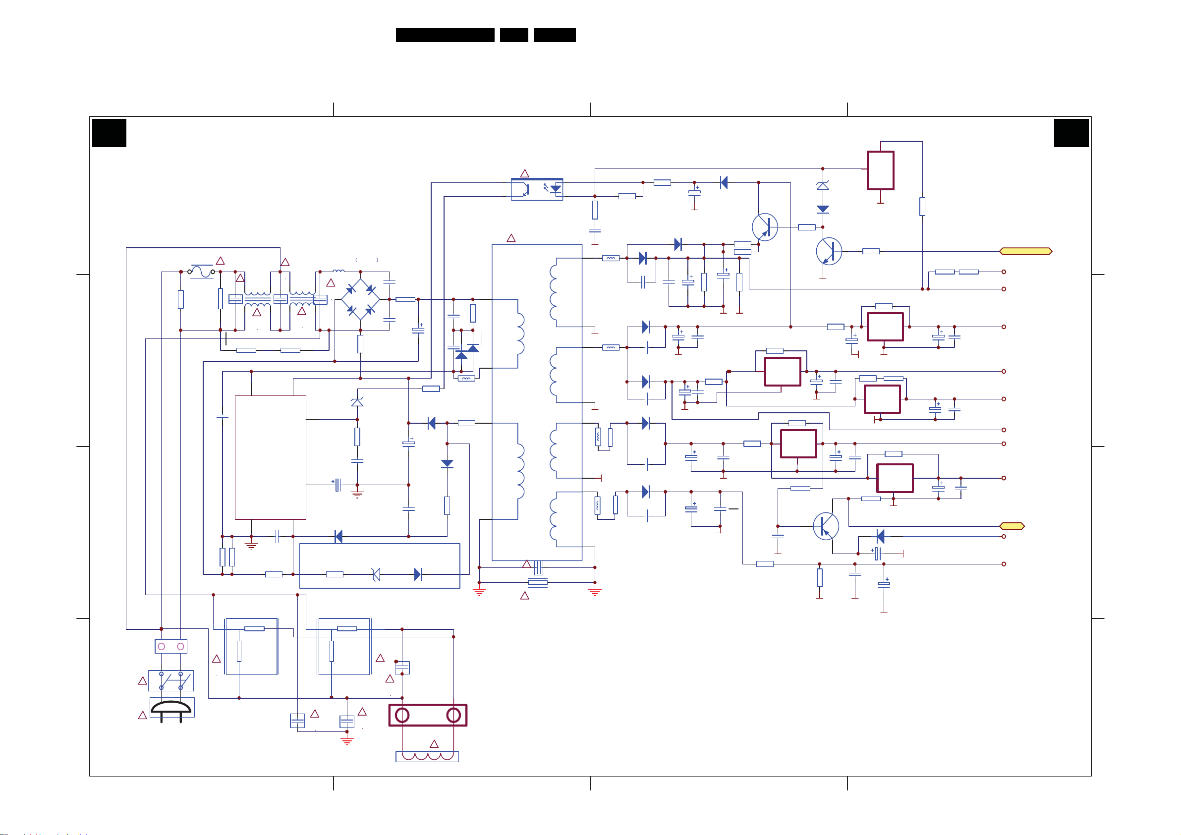
Circuit Diagrams and PWB Layouts
7. Circuit Diagrams and PWB Layouts
Mono Carrier: Power Supply
18SK6.0A CA 7.
321
4
A1 A1
D
C
B
POWER SUPPLY
!
R601
2.2M 1/2W
F60 1T3.15A 250V
VDR601
C613
1000p/2KV
R611
0.82/2W
0.47uF/AC250V
!
C601
0.47uF/AC250V
CMQX0680-3C 680V
RST601
220/1W
R613
0.18/2W
C602
!
GST6 01
4
L601
15mH
!
VCC
FB
L602
15mH
!
GIGA SURGE ABSORBER 300V
1
IC601
D
STR-W6756
OLP/SS
S/GND
3
C615
220p/500V
R612
100/1W
OCP/BD
7
32
L603 (R602)
!
C603
6
C614
1uF/50V
5
R610
18K
28mH 4/15W
BR605
KBJ6J
0.22uF/AC250V
32
D604
EU1Z
4n7/2KV
C607
4n7/2KV
R604
68K/ 2W
ZD601
6V2
R608
1K/1/4W
C612
0.1uF/50V
ZD602
16V
32
C605
R600
5
C609
220uF/450V
R607 1K/1/4W
D605
BA158
C611
10uF/63V
C616
0.0015uF/50V
D606
BA158
C610
0.01uF/1KV
C610A
680pF/1KV
1N5397
FB601
R606
10/1/4W
D603
EU1Z
R609
1K/1W
9
D602
1N5397
D602A
6
2
3
R605
100K/2W
IC603
PC817
T601
BCK4222
!
C619
!
!
!
*
R626
0.0022uF
8.2M /1W
R627
1K/1/6W
R643
10K/1/6W
C660
0.1uF/63V
GND
16
140V
FB623
C635
680pF/2KV
18
GND
4
FB622
14
12V
C632
15
220pF/500V
GND GND
10
7V5
R623
FB621
0.22
C628
11
220pF/500V
GND
12
13V
R624
FB620
13
D626
LG16S
0.01uF/500V
D625
RG2Y
D624 RG2Y
D623
RU4YX
C624
680pF/500V
0.22
R629
1K/1/6W
D627
BA158
C637
C634
3300uF/16V
C633
220pF/500V
GND
C630
1000uF/16V
D622
RU4YX
C640
100uF/50V
GND
C638
220uF/160V
R642
C631
0.01uF/50V
C627
2200uF/16V
C625
1000uF/25V
0.01uF/50V
D628
100K/1/2W
C639
GND
C636
0.01uF/50V
R633
1R5/2W
C629
0.01uF/50V
GND
C626
GND
BA158
R631
120/2W
10uF/160V
GND
D
120/2W
R631A
R628
100K/1/2W
R618
5R1/2W
C653
0.33uF/63V
R619
0.33/2W
Q60 3
A1930
R640 56/2W
IC607
123
L7808
R637 33/2W
123
GND
R635
3K3/1/6W
IC605
L7805
R644
10K/1/6W
Q60 4
A1015
R622
2K7/1/2W
ZD620
5V1
D630
BA158
GND
R625
2R7/2W
C654
1000uF/16V
C649
330uF/16V
GND
C644
470uF/16V
0.01uF/50V
GND
SE130
Q60 2
C2230
C648
0.01uF/50V
R641
51/2W
C645
0.1uF/50V
C411
GND
IC602
1
2
3
GND
R634
22k/1/6W
R636180/2W
IC604
123
L7805
GND
GND
IC608
123
L7805
GND
R638 22/2W
R645
330K/1/6W
100uF/16V
GND
IC606
123
L7805
GND
D631
1N4148
C652
GND
C641
1000uF/25V
R641A
51/2W
R630
3.9K/ 1/ 6W
R301
10K/2W
C642
1000uF/16V
C643
0.1uF/50V
C651
470uF/16V
C650
0.1uF/50V
0.1uF/50V
C646
470uF/16V
Stand-by(from UOC)
J301
+33V
8.2K/ 2W
+140V
+5V_CPU
+5V_U
+13V
+5V_D
C647
5V_A
P_CHK
5V-CPU
+13V(SOUND)
Stand-by(from UOC)
+33V
+140V
+5V_CPU
+8V
+8V
+5V_U
+13V
+5V_D
5V_A
P_CHK
5V-CPU
+13V(SOUND)
D
C
B
A
AC220V
5800-A6P190-00
CN601
SW601
!
!
TH605
!
1
1 2 3 4
1
!
C617
470PFAC400V
TH603
!
!
CN602
C618
470PFAV400V
C608
!
0.1uF/250~500V
!
H602
H_17230_001.eps
260607
A
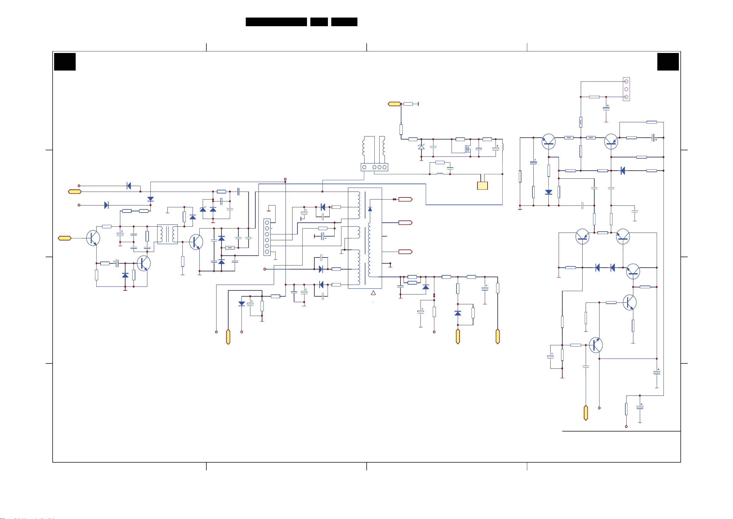
Circuit Diagrams and PWB Layouts
Mono Carrier: Line Deflection
19SK6.0A CA 7.
4321
A2 A2
D
C
HOUT
B
LINE DEFLECTION
D629
R304
180/1/2W
Q301
C1815
R306
68/1/6W
R305
100
1N4148
D301
BA158
C310
10uF/50V
GND
C315
4.7uF/50-100V
D307
IN4148
R302A
5R6/2W
C309
0.001uF/50V
22nF/100V
C313
0.001uF/500V
10K/1/6W
GND
R302
5R6/2W
C314
R309
+8V
FBP
+13V
+8V
FBP
+13V
HOUT
R308
47/2W
D302
BA158
Q302
C2026
GND
T301
H-DRIVER
R310
0.51/2W
GND
R341
12/1/4W
ZD301
7V5
D306
BYW36
GND
Q303
5859
GND
1n/2KV
C302A
1n/2KV
R303
12K/2W
56pF/500V
C301
D303
1N4148
D305
BY459
FB301
C302
D304
211060
+140V
C312
470pF/2KV
C311
0.0047UF/500V
C303
*8n2/2KV
C305
*18n/630V
D311
IN4148
+5V_CPU
H-PRO
+5V_CPU+140V
H-PRO
C304
*3n3/2KV
C323
1uF/50V
-15V
GND
GND
CN302
+15V
+140V
+200V
HEAT
GND
GND
R320
10K/1/6W
R321
10K/1/6W
+15V
C334
0.01uF/50V
GND
C335
1000uF/25V
GND
D308
BA158
C319
22uF/250V
R307 1.7/5W
GND
-15V
D315
RG2Y
+15V
C336
680pF/500V
R311
0.68/2W
C318
680pF/500V
C316
100uF/200V
C331
680pF/500V
R316
0.68/2W
D316
RG2Y
GND
T302
1
10
2
9
8
6
4
5
R315
0.22/2W
CN301
H V
*
!
E/W
12
13
GND
7
C339
0.1uF/250V
EHT
FOCUS
GND
R348
N.C
R339
100/1/6W
R326
3.9K/1/6W
G2
R312
2K/1/4W
R313
2K/1/4W
C320
N.C
GND
GND
8V
ZD302
8V2
D310
BA158
C329
0.001uF/50V
R317
270/1W
L302
*3.5uH
R333
9.1K/1/4W
+15V
R325
68K/1/4W
C322
0.001uF/1KV
D309
4.7K/1/6W
R337
2.7K/1/6W
ABL
ABL
R336
22K/1/ 6W
D313
IN4148
R323
2R2/2W
Q305
F6300
C330
0.01uF/50V
1
2
connect to CON2
C337
N.C
GND
R351
1M/1/2W
C308
4.7uF/50V
L301
*130uH
R338
100K/1/6W
EHT
EHT
GND
R714
56/1W
Q707
2SC4793
C708
100uF/50V
R715
2.7/1/2W
D703
IN4148
R712
1.5K
GND
C702
2.2uF/50V
L702 L703
R716
68K
C707
R713
0.0047uF/100V
1.2K
C705
100pF/50V
Q705
2SA1015Y
R707
1K
R708
33K
R701
3.3K
R702
18K
L701
R718
12K
GND
R724
220/2W
D702
IN4148
R703
470/1W
Q706
2SA1837
R717
68K
R711
22
R709
10
C711
10uF/25 0V
GND
R710
22
D701
IN4 148
R704
150
Q701
2SC1815Y
CN702
R722
2.7/1/2W
D704
IN4148
C706
0.0047uF/500V
GND
Q704
2SC1815Y
Q703
2SC1815Y
GND
R720
1.2K
C704
100pF/50V
R705
1K
Q702
2SC1815Y
R706
68
R721
56/1W
C709
100uF/16V
R719
1.5K
D
C
B
A
5800-A6P190-00
C701
3pF/50V
GND
+15V
+15V
SVM
1 2 3 4
R723
270/2W
+140V
C703
47uF/25 V
GND
GND
C710
10uF/25 0V
H_17230_002.eps
A
260607
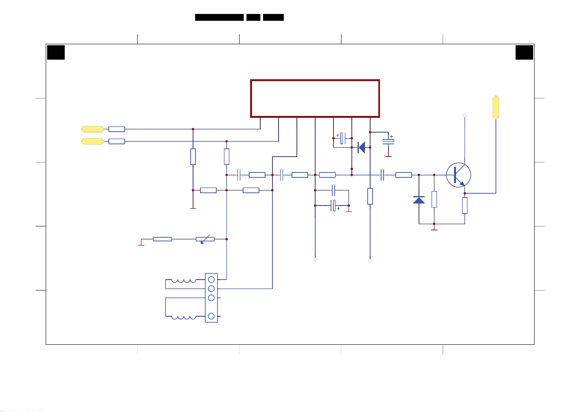
Circuit Diagrams and PWB Layouts
Mono Carrier: Frame Deflection
20SK6.0A CA 7.
E
D
C
A3
FRAME DEFLECTION
J325
V+
V-
J324
100/1/6W
100/1/6W
V+
V-
R330
1K8/1/6W
GND
C328
0.1uF/63V
R327
0.68/2W
IC301
R329
1K8/1/6W
5.6/1/6W
R324
220/2W
7
R322
4321
5
A3
E
TDA4863AJ
INP
INN
6
V-OU T
5
GND4VP23VP32VP1
1
+5V_CPU
D314
BA158
R328
5R6/1/6W
C327
0.1uF/100V
C325
100uF/50V
R342
220/2W
C333
0.01uF/50V
C332
C324
0.33uF/63V
R331
0.68/2W
GND
C326
1000uF/25V
GND
22K/1/6W
R340
D312
IN4148
R318
22K/1/6W
Q304
C1815
R319
1K/1/6W
1000uF/25V
Vs
D
C
B
A
5800-A6P190-00
GND
R327A
15/2W
R327B
10
-15V
+15V
GND
B
CN301
V
H
A
H_17230_003.eps
260607
1 2 3 45
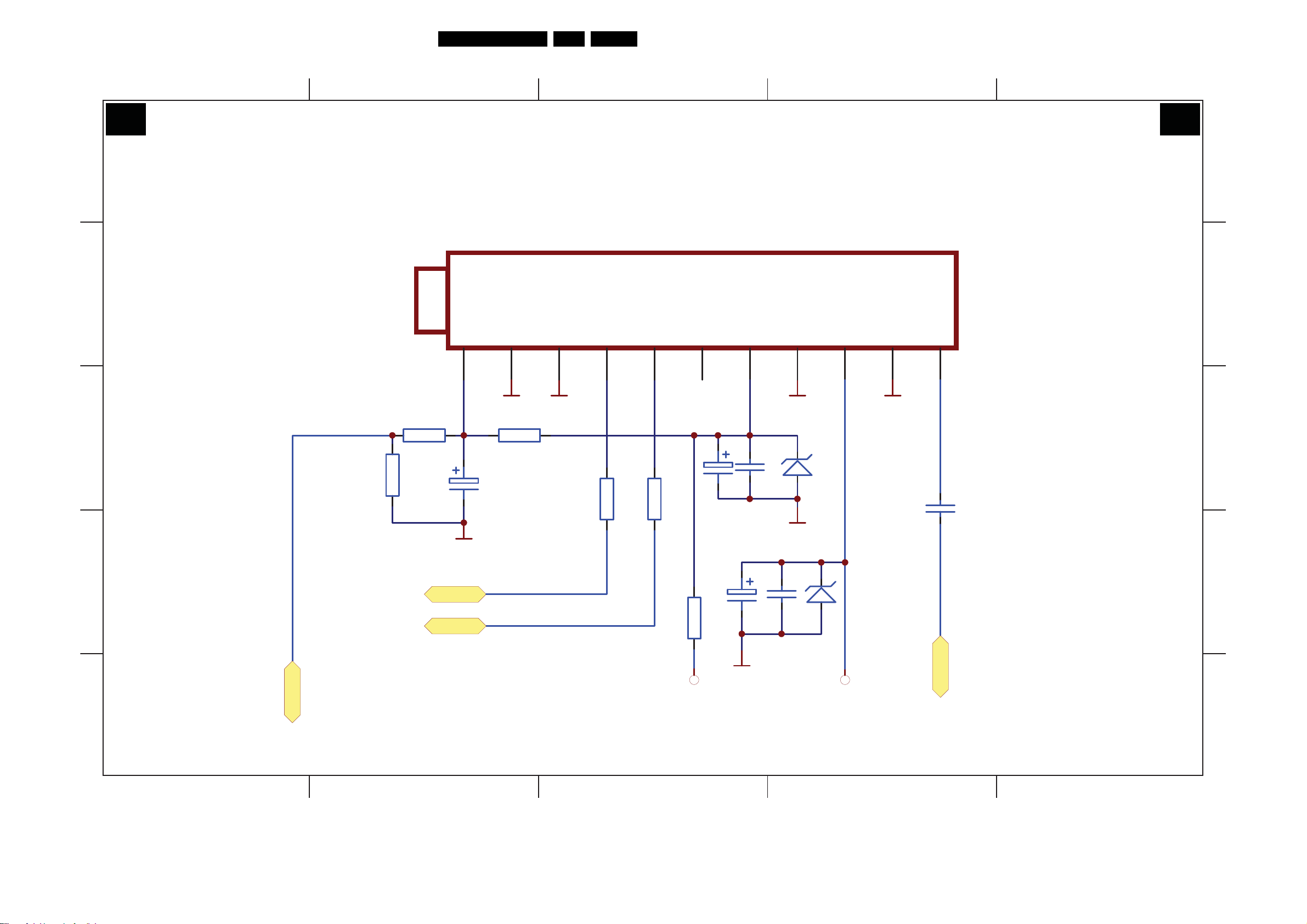
Mono Carrier: Tuner IF
Circuit Diagrams and PWB Layouts
21SK6.0A CA 7.
E
D
A4
TUNER IF
TUNER
R112
6K8/1/6W
4321
5
A4
E
D
AGC
1
GND2AS
GND
R111
SCL
3
SDA
5
6
GND C105
47uF/16V
+5V7GND8+33V9IFGND10IF
11
GND
GND
ZD101
C
10k/1/6W
5V1
C
R113
100K/1/6W
C107
4.7uF/16V
C106
0.01uF/50V
GND
B
SCL1
SCL1
R107 100/1/6W
R108 100/1/6W
22uF/50V
C102
GND
IC003
KA 33
C101
0.01uF/50V
B
IF
AGC
SDA1
SDA1
R110
+8V
+8V
27/1W
C103
0.01uF/50V
GND
+33V
IF
+33V
AGC
A
A
5800-A6P190-00
H_17230_004.eps
260607
1 2 3 45
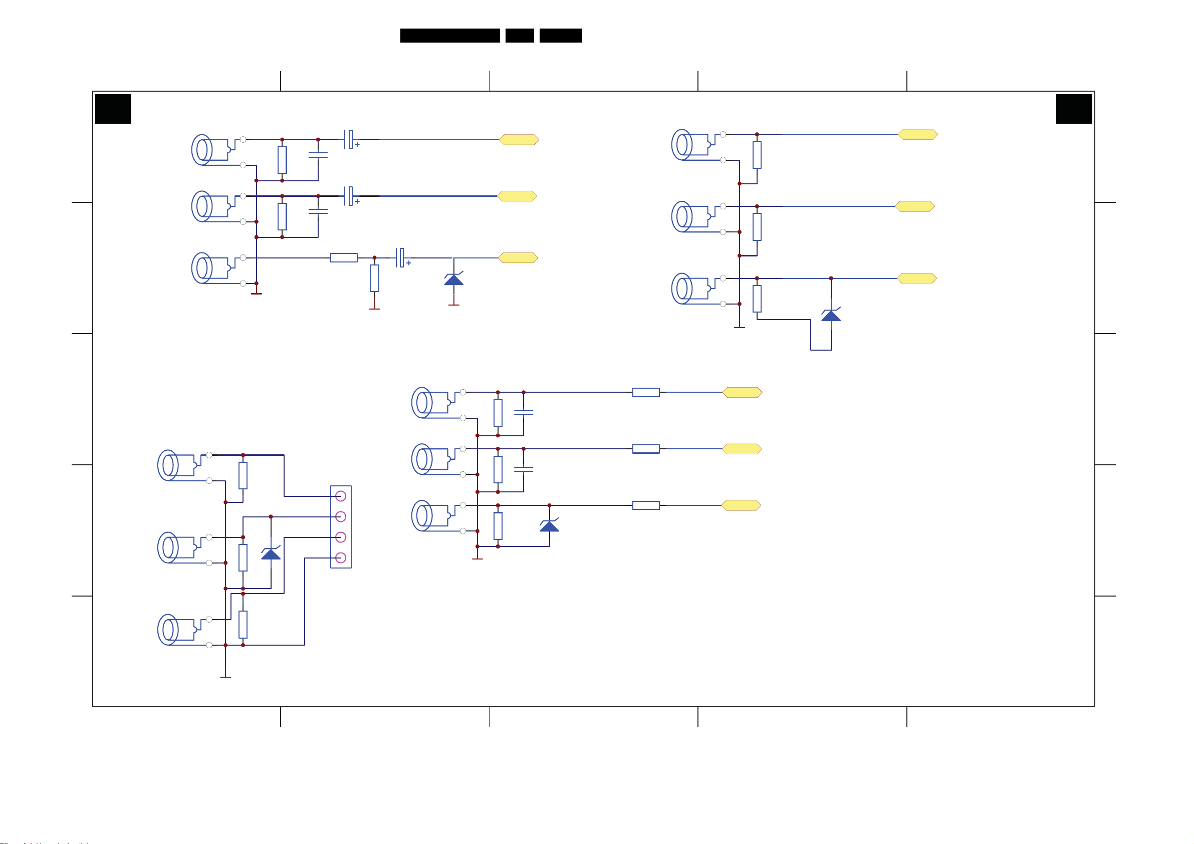
Circuit Diagrams and PWB Layouts
Mono Carrier: AV I/O Interface
22SK6.0A CA 7.
E
D
A5
AV I/O
R0
L0
V0
R428
240K/1/6W
GND
R427
240K/1/6W
C429
100pF/50V
C428
100pF/50V
R441
75/1/6W
C421
10uF/16V
C420
10uF/16V
R442
470K/1/6W
GND
C422
470uF/16V
GND
D420
8.2V
R0
L0
V0
Cr
Cb
Y
GND
R440
75/1/6W
R438
75/1/6W
R439
75/1/6W
4321
5
A5
Cr
Cb
Y
D432
8.2V
E
D
C
B
A
5800-A6P190-00
R431
240K/1/6W
C431
R2
R435
Pr
Y
Pb
GND
1 2 3 45
75/1/6W
D430
8.2V
R436
75/1/6W
R437
75/1/6W
Pr
Y
Pb
GND
H403
1
2
3
4
L2
V2
R432 240K/1/6W
R434
75/1/6W
GND
100pF/50V
C432
100pF/50V
D424
8.2V
R430
39K/1/6W
R429
39K/1/6W
R433
220/1/6W
R2
L2
V2
H_17230_005.eps
260607
C
B
A
 Loading...