

PHILIPS SK5.1L CA Service Manual

Colour Television Chassis
SK5.1L
CA
H_17220_000.eps
210607
Contents Page
1. Technical Specifications, Connections, and Chassis
Overview 2
2. Safety Instructions, Warnings, and Notes 4
3. Directions for Use 5
4. Mechanical Instructions 6
5. Service Modes, Error Codes, and Fault Finding 8
6. Block Diagrams, Test Point Overview, and
Waveforms
Block Diagram Chassis 9
Schematic Overview Chassis 10
7. Circuit Diagrams and PWB Layouts
Mono Carrier: Power Supply (A1) 11 18-19
Mono Carrier: Line Deflection (A2) 12 18-19
Mono Carrier: Frame Deflection (A3) 13 18-19
Mono Carrier: Tuner IF (A4) 14 18-19
Mono Carrier: AV Switch (A5) 15 18-19
Mono Carrier: Tone Control (Optional) (A6) 16 18-19
Mono Carrier: Audio Amplifier (A7) 17 18-19
CRT Board (B) 20 18-19
Keyboard Control Panel (D) 21 22
Side A/V Panel (G) 23 23
8. Alignments 25
9. Circuit Descriptions, Abbreviation List, and IC Data
Sheets 30
Abbreviation List 31
IC Data Sheets 32
10. Spare Parts List 45
11. Revision List 48
©
Copyright 2008 Philips Consumer Electronics B.V. Eindhoven, The Netherlands.
All rights reserved. No part of this publication may be reproduced, stored in a
retrieval system or transmitted, in any form or by any means, electronic,
mechanical, photocopying, or otherwise without the prior permission of Philips.
Published by JY 0864 BU CD Consumer Care Printed in the Netherlands Subject to modification EN 3122 785 17880
EN 2 SK5.1L CA1.
Technical Specifications, Connections, and Chassis Overview
1. Technical Specifications, Connections, and Chassis Overview
Index of this chapter:
1.1 Technical Specifications
1.2 Connection Overview
1.3 Chassis Overview (Mechanical chassis)
Note: Data below can deviate slightly from the actual situation,
due to the different set executions.
1.1 Technical Specifications
1.1.1 Vision
Display type : CRT
Screen size : 29” (72 cm), 4:3
Tuning system : PLL
TV Colour systems : NTSC, PAL M, N
Video playback : NTSC, PAL all
versions
Presets/channels : 181 channels
Tuner bands : VHF
: UHF
1.1.2 Sound
Sound systems : Stereo, SAP
Maximum power (W
1.1.3 Miscellaneous
):2 x 5
RMS
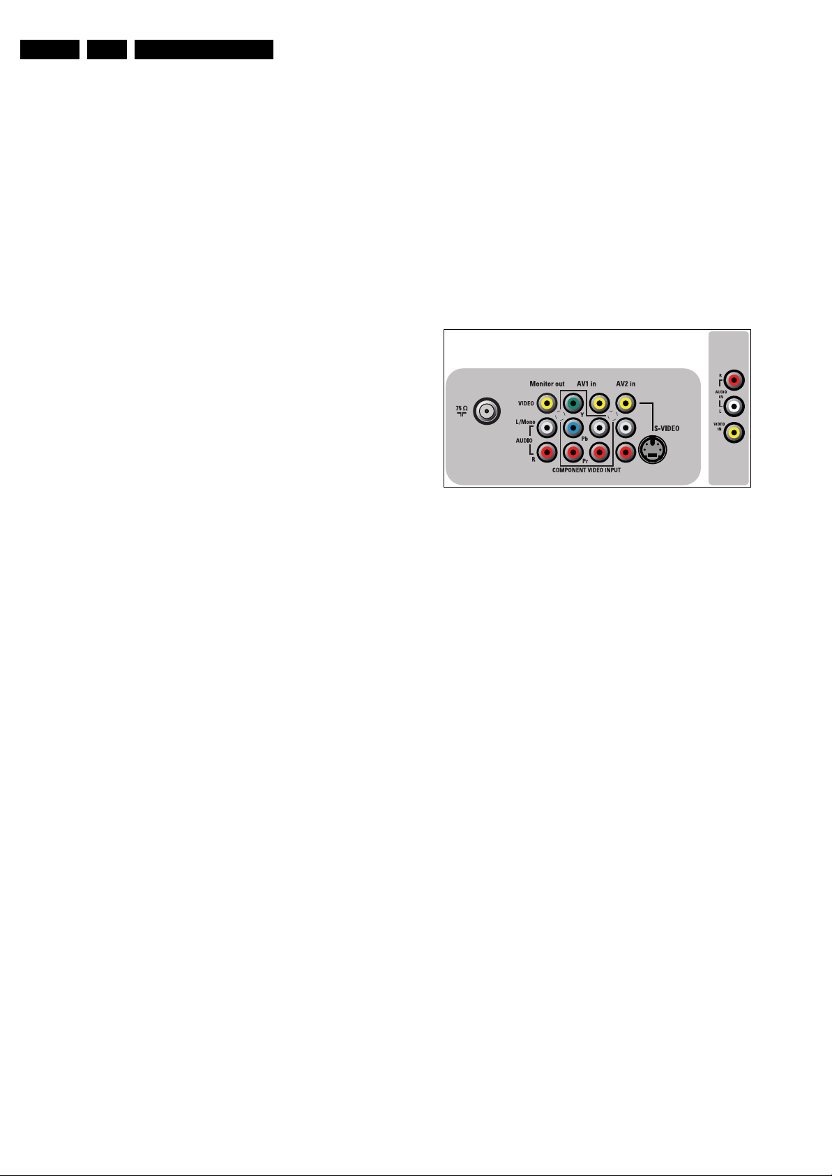
1.2 Connection Overview
Note: The following connector colour abbreviations are used
(acc. to DIN/IEC 757): Bk= Black, Bu= Blue, Gn= Green, Gy=
Grey, Rd= Red, Wh= White, and Ye= Yellow.
1.2.1 Front / Side Connections
Side in, Cinch: Video CVBS - In, Audio - In
Ye -Video CVBS 1 V
Wh - Audio L 0.5 V
Rd - Audio R 0.5 V
Figure 1-1 Rear and Side Connections
/ 75 ohm jq
PP
/ 10 kohm jq
RMS
/ 10 kohm jq
RMS
H_17880_001.eps
190308
Power supply:
- Mains voltage (V
) : 100 - 240
AC
- Mains frequency (Hz) : 50 / 60
Ambient conditions:
- Temperature range (°C) : -5 to +45
- Maximum humidity : 90% R.H.
Power consumption
- Normal operation (W) : ≈ 105
- Stand-by (W) : < 1
Dimensions (W × H × D mm) : 781 × 586 × 400
Weight (kg) : 40.5
1.2.2 Rear Connections
Aerial - In
- - F-connector Coax, 75 ohm D
Monitor out, Cinch: Video CVBS - Out, Audio - Out
Ye - Video CVBS 1 V
Wh - Audio L 0.5 V
Rd - Audio R 0.5 V
/ 75 ohm kq
PP
/10 kohm kq
RMS
/ 10 kohm kq
RMS
AV1 in, Cinch: Video YPbPr - In
Gn - Video Y 1 V
Bu - Video Pb 0.7 V
Rd - Video Pr 0.7 V
Ye - Video CVBS 1 V
Wh - Audio L 0.5 V
Rd - Audio R 0.5 V
/ 75 ohm jq
PP
/ 75 ohm jq
PP
/ 75 ohm jq
PP
/ 75 ohm kq
PP
/ 10 kohm jq
RMS
/ 10 kohm jq
RMS
AV2 in, Cinch: Video CVBS - In, Audio - In
Ye - Video CVBS 1 V
Wh - Audio L 0.5 V
Rd - Audio R 0.5 V
/ 75 ohm jq
PP
/ 10 kohm jq
RMS
/ 10 kohm jq
RMS
AV2 in, S-Video (Hosiden): Video Y/C - In
1 -Ground Y Gnd H
2 -Ground C Gnd H
3 -Video Y 1 V
4 -Video C 0.3 V
/ 75 ohm j
PP
P / 75 ohm j
PP
Technical Specifications, Connections, and Chassis Overview
1.3 Chassis Overview (Mechanical chassis)
CONTROL PANEL
D
CRT BOARD
B
EN 3SK5.1L CA 1.
Figure 1-2 PWB location
MONO CARRIER
SIDE AV PANEL
A
G
POWER SUPPLY
A1
A2
LINE DEFLECTION
A3
FRAME DEFLECTION
A4
TUNER
A5
AV SWITCH
A6
AUDIO AMPLIFIER
A7
CPU & DECODER
I_17880_002.eps
210308
EN 4 SK5.1L CA2.
Safety Instructions, Warnings, and Notes
2. Safety Instructions, Warnings, and Notes
Index of this chapter:
2.1 Safety Instructions
2.2 Maintenance Instructions
2.3 Warnings
2.4 Notes
2.1 Safety Instructions
Safety regulations require the following during a repair:
• Connect the set to the Mains/AC Power via an isolation
transformer (> 800 VA).
• Replace safety components, indicated by the symbol h,
only by components identical to the original ones. Any
other component substitution (other than original type) may
increase risk of fire or electrical shock hazard.
• Wear safety goggles when you replace the CRT.
Safety regulations require that after a repair, the set must be
returned in its original condition. Pay in particular attention to
the following points:
• General repair instruction: as a strict precaution, we advise
you to re-solder the solder connections through which the
horizontal deflection current flows. In particular this is valid
for the:
1. Pins of the line output transformer (LOT).
2. Fly-back capacitor(s).
3. S-correction capacitor(s).
4. Line output transistor.
5. Pins of the connector with wires to the deflection coil.
6. Other components through which the deflection current
flows.
Note: This re-soldering is advised to prevent bad connections
due to metal fatigue in solder connections, and is therefore only
necessary for television sets more than two years old.
• Route the wire trees and EHT cable correctly and secure
them with the mounted cable clamps.
• Check the insulation of the Mains/AC Power lead for
external damage.
• Check the strain relief of the Mains/AC Power cord for
proper function, to prevent the cord from touching the CRT,
hot components, or heat sinks.
• Check the electrical DC resistance between the Mains/AC
Power plug and the secondary side (only for sets that have
a Mains/AC Power isolated power supply):
1. Unplug the Mains/AC Power cord and connect a wire
between the two pins of the Mains/AC Power plug.
2. Set the Mains/AC Power switch to the “on” position
(keep the Mains/AC Power cord unplugged!).
3. Measure the resistance value between the pins of the
Mains/AC Power plug and the metal shielding of the
tuner or the aerial connection on the set. The reading
should be between 4.5 Mohm and 12 Mohm.
4. Switch “off” the set, and remove the wire between the
two pins of the Mains/AC Power plug.
• Check the cabinet for defects, to prevent touching of any
inner parts by the customer.
2.2 Maintenance Instructions
We recommend a maintenance inspection carried out by
qualified service personnel. The interval depends on the usage
conditions:
• When a customer uses the set under normal
circumstances, for example in a living room, the
recommended interval is three to five years.
• When a customer uses the set in an environment with
higher dust, grease, or moisture levels, for example in a
kitchen, the recommended interval is one year.
• The maintenance inspection includes the following actions:
1. Perform the “general repair instruction” noted above.
2. Clean the power supply and deflection circuitry on the
chassis.
3. Clean the picture tube panel and the neck of the picture
tube.
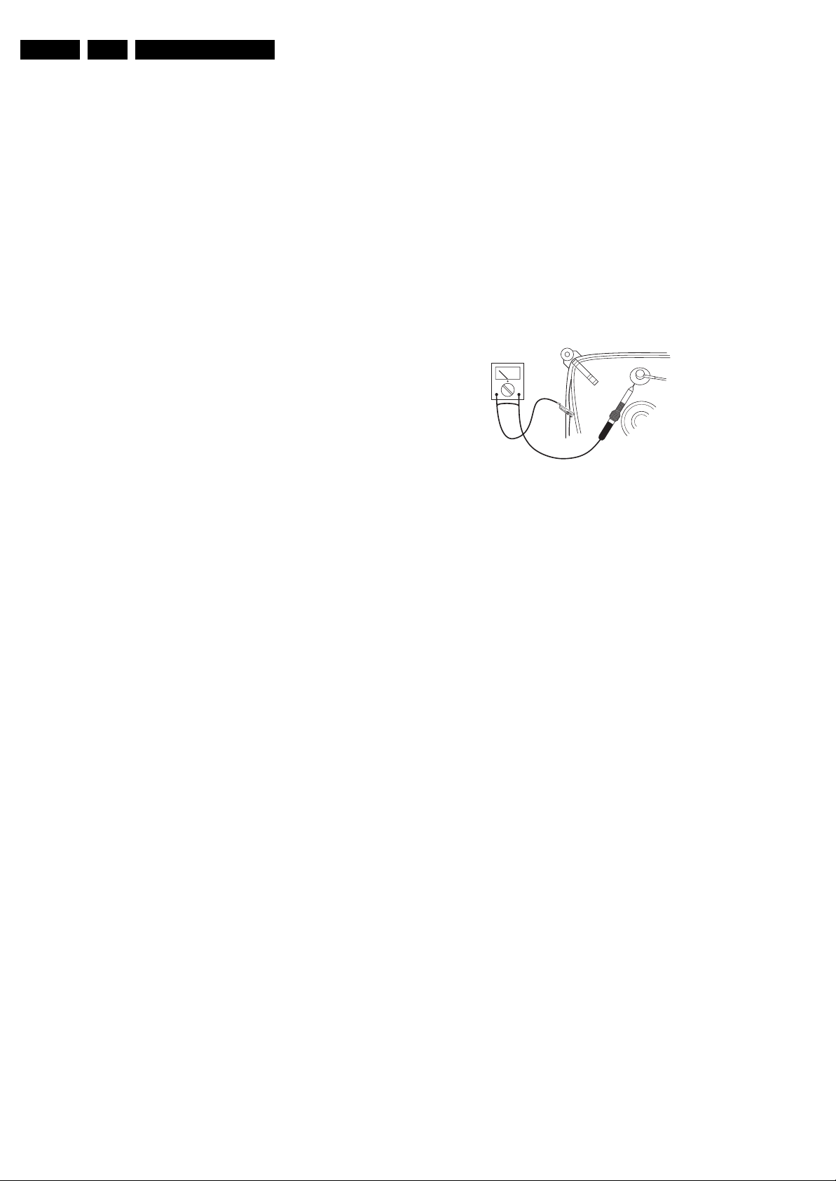
2.3 Warnings
• In order to prevent damage to ICs and transistors, avoid all
high voltage flashovers. In order to prevent damage to the
picture tube, use the method shown in figure “Discharge
picture tube”, to discharge the picture tube. Use a high
voltage probe and a multi-meter (position V
until the meter reading is 0 V (after approx. 30 s).
V
E_06532_007.eps
250304
Figure 2-1 Discharge picture tube
• All ICs and many other semiconductors are susceptible to
electrostatic discharges (ESD w). Careless handling
during repair can reduce life drastically. Make sure that,
during repair, you are connected with the same potential as
the mass of the set by a wristband with resistance. Keep
components and tools also at this same potential.
• Be careful during measurements in the high voltage
section.
• Never replace modules or other components while the unit
is switched “on”.
• When you align the set, use plastic rather than metal tools.
This will prevent any short circuits and prevents circuits
from becoming unstable.
2.4 Notes
2.4.1 General
• Measure the voltages and waveforms with regard to the
chassis (= tuner) ground (H), or hot ground (I), depending
on the tested area of circuitry. The voltages and waveforms
shown in the diagrams are indicative. Measure them in the
Service Default Mode (see chapter 5) with a colour bar
signal and stereo sound (L: 3 kHz, R: 1 kHz unless stated
otherwise) and picture carrier at 475.25 MHz for PAL, or
61.25 MHz for NTSC (channel 3).
• Where necessary, measure the waveforms and voltages
with (D) and without (E) aerial signal. Measure the
voltages in the power supply section both in normal
operation (G) and in stand-by (F). These values are
indicated by means of the appropriate symbols.
• The semiconductors indicated in the circuit diagram and in
the parts lists, are interchangeable per position with the
semiconductors in the unit, irrespective of the type
indication on these semiconductors.
• Manufactured under license from Dolby Laboratories.
“Dolby”, “Pro Logic” and the “double-D symbol”, are
trademarks of Dolby Laboratories.
). Discharge
DC

Directions for Use
EN 5SK5.1L CA 3.
2.4.2 Schematic Notes
• All resistor values are in ohms, and the value multiplier is
often used to indicate the decimal point location (e.g. 2K2
indicates 2.2 kohm).
• Resistor values with no multiplier may be indicated with
either an “E” or an “R” (e.g. 220E or 220R indicates
220 ohm).
• All capacitor values are given in micro-farads (μ = × 10
nano-farads (n = × 10
• Capacitor values may also use the value multiplier as the
decimal point indication (e.g. 2p2 indicates 2.2 pF).
• An “asterisk” (*) indicates component usage varies. Refer
to the diversity tables for the correct values.
• The correct component values are listed in the Spare Parts
List. Therefore, always check this list when there is any
doubt.
2.4.3 Lead-free Soldering
Due to lead-free technology some rules have to be respected
by the workshop during a repair:
• Use only lead-free soldering tin Philips SAC305 with order
code 0622 149 00106. If lead-free solder paste is required,
please contact the manufacturer of your soldering
equipment. In general, use of solder paste within
workshops should be avoided because paste is not easy to
store and to handle.
• Use only adequate solder tools applicable for lead-free
soldering tin. The solder tool must be able:
– To reach a solder-tip temperature of at least 400°C.
– To stabilize the adjusted temperature at the solder-tip.
– To exchange solder-tips for different applications.
• Adjust your solder tool so that a temperature of around
360°C - 380°C is reached and stabilized at the solder joint.
Heating time of the solder-joint should not exceed ~ 4 sec.
Avoid temperatures above 400°C, otherwise wear-out of
tips will increase drastically and flux-fluid will be destroyed.
To avoid wear-out of tips, switch “off” unused equipment or
reduce heat.
• Mix of lead-free soldering tin/parts with leaded soldering
tin/parts is possible but PHILIPS recommends strongly to
-9
), or pico-farads (p = × 10
-12
avoid mixed regimes. If this cannot be avoided, carefully
clear the solder-joint from old tin and re-solder with new tin.
2.4.4 Alternative BOM identification
In September 2003, Philips CE introduced a change in the way
the serial number (or production number, see Figure 2-2) is
-6
),
).
composed. From this date on, the third digit in the serial
number (example: AG2B0335000001) indicates the number of
the alternative BOM (Bill of Materials used for producing the
specific model of TV set). It is possible that the same TV model
on the market is produced with e.g. two different types of
displays, coming from two different O.E.M.s.
By looking at the third digit of the serial number, the service
technician can see if there is more than one type of B.O.M.
used in the production of the TV set he is working with. He can
then consult the At Your Service Web site, where he can type
in the Commercial Type Version Number of the TV set (e.g.
28PW9515/12), after which a screen will appear that gives
information about the number of alternative B.O.M.s used.
If the third digit of the serial number contains the number 1
(example: AG1B033500001), then there is only one B.O.M.
version of the TV set on the market. If the third digit is a 2
(example: AG2B0335000001), then there are two different
B.O.M.s. Information about this is important for ordering the
correct spare parts!
For the third digit, the numbers 1...9 and the characters A...Z
can be used, so in total: 9 plus 26 = 35 different B.O.M.s can
be indicated by the third digit of the serial number.
2.4.5 Practical Service Precautions
• It makes sense to avoid exposure to electrical shock.
While some sources are expected to have a possible
dangerous impact, others of quite high potential are of
limited current and are sometimes held in less regard.
• Always respect voltages. While some may not be
dangerous in themselves, they can cause unexpected
reactions that are best avoided. Before reaching into a
powered TV set, it is best to test the high voltage insulation.
It is easy to do, and is a good service precaution.
3. Directions for Use
You can download this information from the following websites:
http://www.philips.com/support
http://www.p4c.philips.com
EN 6 SK5.1L CA4.
Mechanical Instructions
4. Mechanical Instructions
Index of this chapter:
4.1 Set Disassembly
4.2 Assembly / Board Removal
4.3 Set Re-assembly
Note: Figures below can deviate slightly from the actual
situation, due to the different set executions.
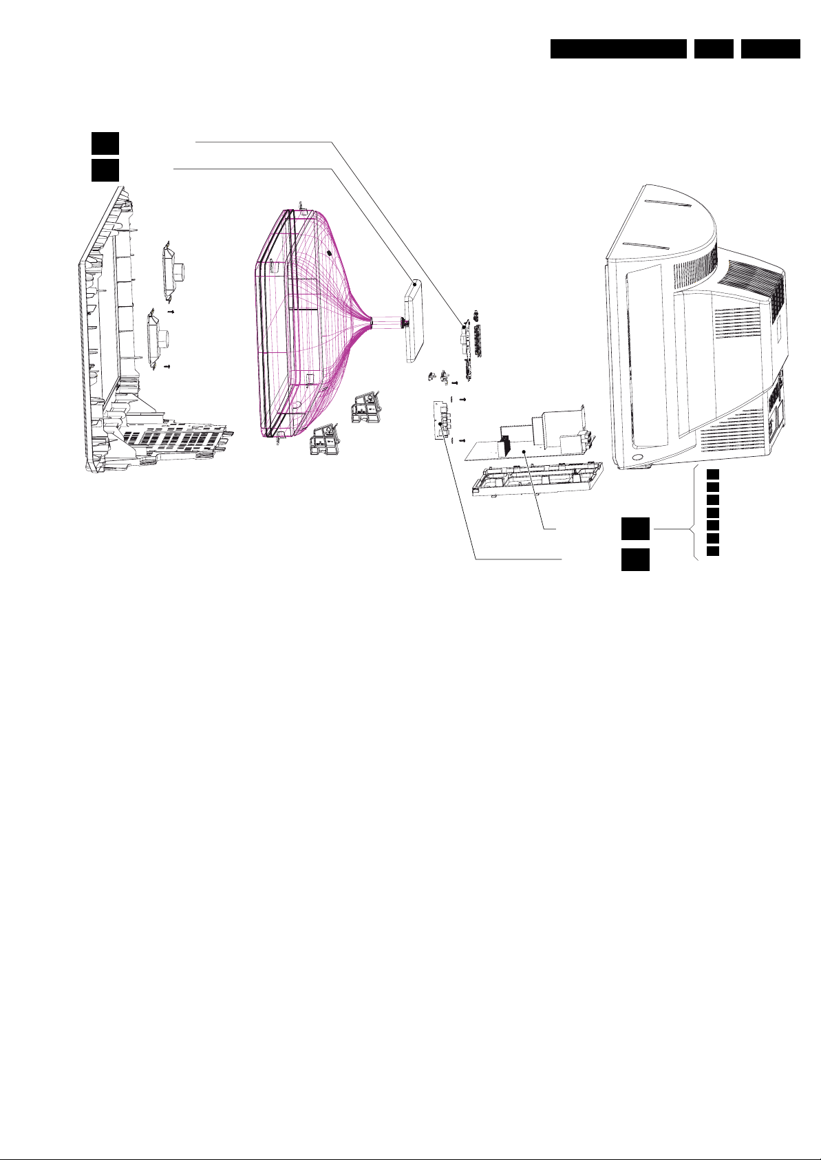
4.1 Set Disassembly
Follow the disassemble instructions in described order.
4.1.1 Rear Cover Removal
Warning: disconnect the mains power cord before you remove
the rear cover.
1. Remove all the fixation screws of the rear cover.
2. Now, pull the rear cover backwards and remove it.
4.2 Assembly / Board Removal
4.2.1 Power Switch and Control Panel removal
1. From the mono carrier disconnect the main power and the
keyboard circuit cables. Release the main power cord and
the keyboard circuit cable from it’s strain reliefs.
2. Then, remove the two fixation screws [1] of the power
switch and control panel and remove the board.
Figure 4-1 Rear Cover removal
I_17880_005.eps
210308
I_17880_004.eps
1
210308
Figure 4-2 Power Switch and Control Panel removal
4.2.2 Side I/O Panel removal
Mechanical Instructions
1
EN 7SK5.1L CA 4.
Figure 4-3 Side-I/O panel removal
1. Disconnect the side panel cable from the mono carrier and
remove the cable from it’s strain reliefs.
2. Then, remove the two fixation screws [1] and remove the
board.
When defective replace the whole unit.
4.3 Set Re-assembly
To re-assemble the whole set, do all processes in reverse
order.
Be sure that, before the rear cover is mounted:
• The mains cord is positioned correctly in its guiding
brackets (make sure that the strain reliefs are replaced in
its correct position and that it will function correctly!).
• All wires/cables are returned in their original positions.
I_17880_003.eps
270308

EN 8 SK5.1L CA5.
Service Modes, Error Codes, and Fault Finding
5. Service Modes, Error Codes, and Fault Finding
Index of this chapter:
5.1 Test Points
5.2 Service Modes
5.3 Error Codes
5.4 Fault Finding
5.1 Test Points
See chapter 6 “Block Diagrams, Testpoint Overviews, and
Waveforms”.
Perform measurements under the following conditions:
• Service Default Mode.
• Video: colour bar signal.
• Audio: 3 kHz left, 1 kHz right.
5.2 Service Modes
This chassis does not contain a specific Service Mode. Service
and Alignment of the TV set can be done via the Factory Mode
by the service technician, see further down in this manual.
5.3 Error Codes
Not applicable.
5.4.6 Picture not or incorrect Coloured
• Check the circuit from IC101 to R.G.B. three gun circuit.
• Check the IC soldering and relevant circuitry on physical
damage or check for defective capacitors.
5.4.7 Picture with Horizontal Bright Line and Sound
Check both supply voltages of vertical IC301 and relevant
circuitry on correctness. Also check the vertical synchronizing
signal from IC101.
5.4.8 Remote Control Malfunction
Check the voltage on pin 64 of IC101. The normal value should
be 5.15 V. If this is correct check front control panels soldering
connections. If can't be solved, check the remote control,
crystal or transmitting diode of the remote control are in good
condition.
5.4.9 No Sound
Check power supply of sound IC (IC760, TFA9842) and
relevant circuitry. Check as well the BTSC board, check the
power supply of IC851 and relevant output signal pins 21 and
27 of this IC. Do not exclude IC801 and/or IC402 to be
defective. If needed replace the speakers.
5.4 Fault Finding
5.4.1 Power on Failure
Check whether the power supply is working properly and
whether the values of voltages normal. If those are correct,
check line transistor and transformer are working properly or
check fore or back line for defects.
5.4.2 Horizontal Deflection Transistor Defective: No Picture, No Sound.
To find the fault for a defect horizontal deflection transistor
please check the following items:
• Over voltage to breakdown.
• Over current to burn.
• Horizontal frequency too low.
• Horizontal drive inefficient.
5.4.3 Picture Interference
• Check if the signal line contact is good.
• Change Tuner if is necessary.
5.4.4 Can't find any TV program
Checking method: Check the closed circuit from tuner to
picture decoder IC to detect whether there are defective
components. Or check whether the resistance of R111, R112,
R113 and R114 has increased which also could cause the
problem.
5.4.10 Poor Sound Quality
Check the sound system after searching the channel which
should set at NTSC or AUTO. If still has problem, check
accompany board circuit on chassis good or not.
5.4.5 No Good Picture or Double Image
Check the correctness of the signal from IF1/IF2 to Q101 and
relevant circuit. In this case the problem can be Q101 and/or
SAW101.
Block Diagrams, Test Point Overview, and Waveforms
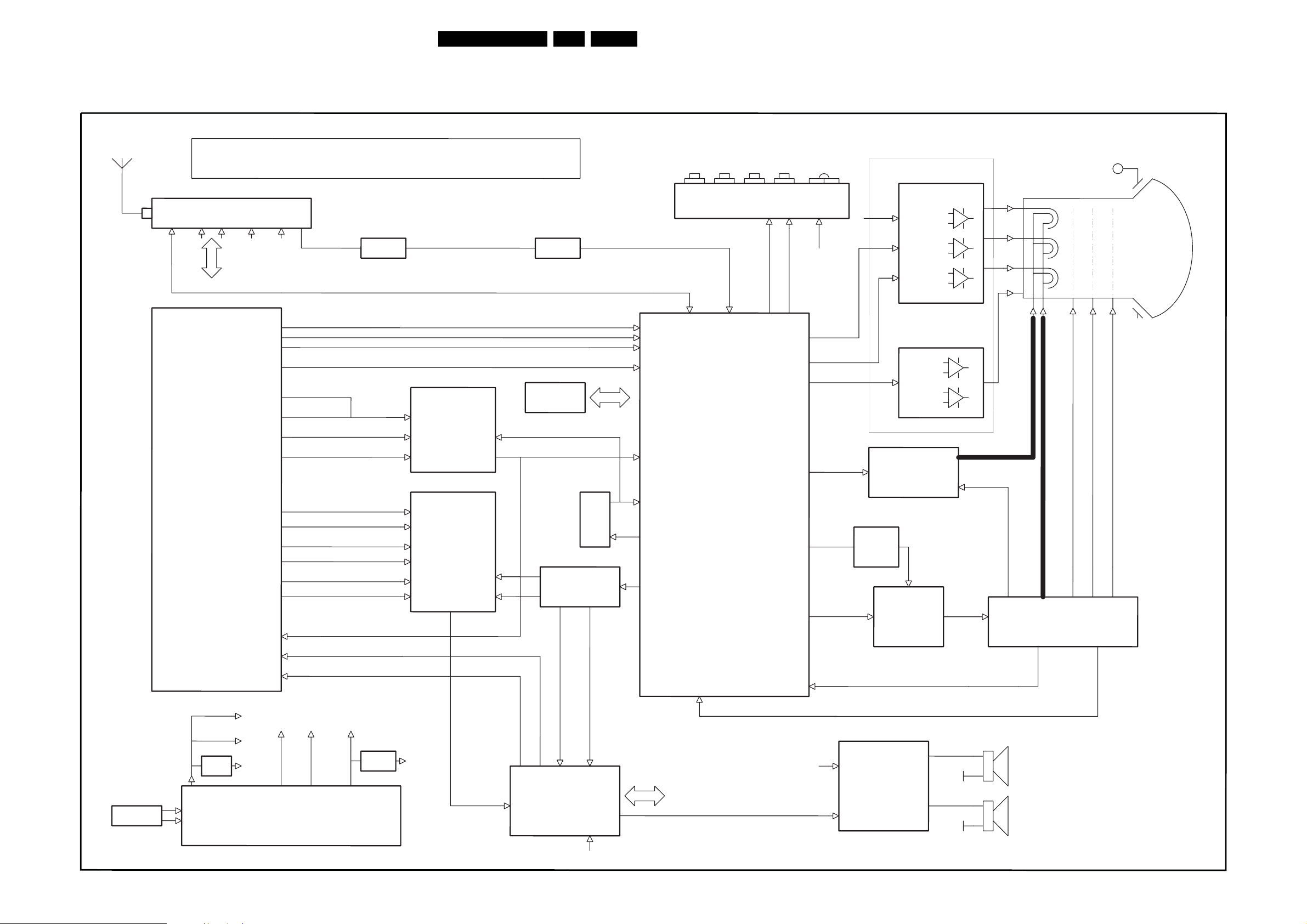
6. Block Diagrams, Test Point Overview, and Waveforms
Block Diagram Chassis
9SK5.1L CA 6.
5P20 29SL7 DIAGRAM(PHILIPS)
TUNER
AGC
YUVINPUT
S-VIDEOINPUT
FRONT/SIDEAV INTUT
AV IN/OUT(BACK)
C2I
5V 33VSCL SDA
+5V
VOUT
LOUT
ROUT
11
+33V
IF
V
Y
U
C
S-VIDEOY
AV2
AV1
SIDE AV
AV1R/YUVR
AV1L/ YUVL
AV2R/S-VIDEOR
AV2L/ S-VIDEOL
SIDE AV R
SIDE AV L
PRE-IF
4
5
2
14
5
11
4
15
2
IC761
HCF4052
IC762
HCF4052
3/13 OUT
1
3
4
11
TV IN
Q1976M
IC102
24C08
29 30
IC740
TDA9850AH
21 27
X4.5B
SDASCL
EHT
KEYBOARD/REMOTELCONTROL
KEY REM +5V
+5V
46
47
48
4
2
I
C
2(SCL)
3(SDA)
42(Y/CVBSIN)
40(CVBSIN)
38(V_OUT)
28
44 (TV AUDIOL\R)
27
GEOMETRYCONTROL
80C51MICROCONTROLLER
23/24
IC101
TDA93XXPS/N2/5I
(PAL/NTSC)
SOURCESWITCHING
SOUNDCONTROL
SYNCPROCESSING
VIF
RGBPROCESSING
64K ROM
2K RAM
10 PAGETELETEXT
ONSCREENDISPLAY
AFC
764
51/52/53
50
21/22
20
33
R/G/B_OUT
2.47V
BLK
V_OUT
EW
H_OUT
ABL
49
6/7
VERTIALDRIVE
V_DEFLECTION
Q440
CS630F
TDA9365
H_AMP
+8V
R/G/B
BLK
SVM44
IC301
EW
N401
D2553
Q501
Q502
Q503
Q504
Q505
Q506
Q507
Q508
Q509
Q906
Q907
5
1/7
KB
KG
KR
SVM
+/-16V
G1 G2 G3
H_DEFLECTION
HEATER
T402
FBT
ABL SC
SCREEN
EHT
ACINPUT
AC90--260V
+3.3V
+5V
7808
+12V +19V +110V
+8V
MAINPOWER
+135V
+22V
IC601
(W6556A)
+45V
+45V
KA33V
+33V
28/30
5 3
IC851
TDA9859H
HI-FI AUDIO
+8V
16(SCL)
17(SDA)
15/18
6
L_OUT
+22V
2
I
C
L/ R
9
1\4
IC760
TDA9842
BTL AUDIOAMP
2
8
VCC
R_OUT
VCC
I_17880_009.eps
270308
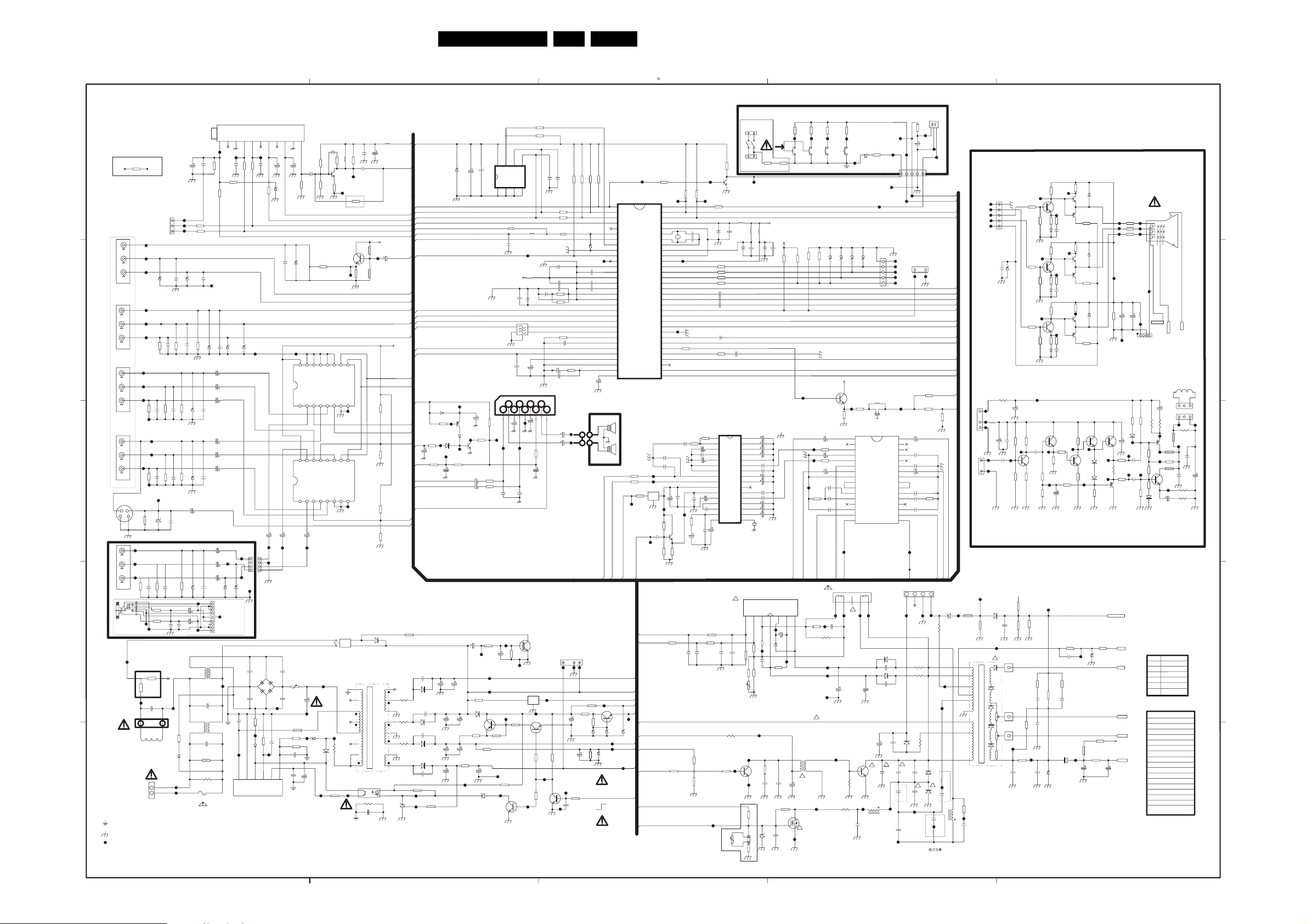
Block Diagrams, Test Point Overview, and Waveforms
Schematic Overview Chassis
1
10SK5.1L CA 6.
2
3
4
5
KEYBOARDCIRCUIT
6
7
PTC
IC102
n.c.
3
2
R122
10K
C152
+8
V_VCC
C120
0.1uF/63V
1
2
2
3
RI RO
T747 T748
C76 5
4700PF
T617
C639
R64 3
47uF
47K
T625
R649
2K2
1K
R136 3.3K
R1171K
5
SCL
SDA
C10 8
L107
10uH
C11 9
+
10uF/16V
6
4
5
C137
10uF/16V
C767
220uF
Q625
C1815
C107
100pF
100pF
R133
R134
R135
47
C12 9
+
10uF/ 16V
C128
10nF
C132
4n7
C133
+
R13818K
1uF/50V
R138A100K
R151
39K
C138
180pF
C139
330pF
IC760
8
TFA9842AJ
9
7
Lout
C769
470uF
C768
470uF
R771
10K
24C08
Vss
A2
4
T116
L104
10uH
SAW101
3
C136
56P
4
5
Lin
C76 4
47uF
T749
C761
1uF/50V
C766
4700PF
1
T641
T618
IC104
L7808
+12V
Q621
C1815
T640
T621
In Out
Gnd
T622
Q622
C2230
R648
R635
22K
22K
T634
T635
R634
10K
Q623
C1815
T633
T636
100
100
C135
0.1uF/ 6 3V
R139
2.7K
T750
T751
2
C634
0.1uF/50V
R132
R131
R130
R145
3.3K
3.3K
3.3K
22K
1
STANDBY
2
L
SC
3
SDA
4
AV3/T UNING
5
SC
ARTID
6
KEY
7
VOL
8
ZD103
BAND
8V2
9
Vss C/P
10
MUTE
11
PAL/NTSC
T117
12
220nF
220nF
2200pF
C140
4.7uF/16V
VssA
13
SECPLL
14
Vp2
15
DECDIG
16
PH2LF
17
PH1LF
18
GND3
19
DECBG
20
AVL/ EWD
21
VDRB
22
VDRA
23
IF1
24
IF2
25
IREF
26
VSC
27
TUNE R AGC
28
AUDEEM/ SIF1
29
DEC SDEM/SIF2
30
GND2
31
SNDPLL/SI FAGC
32
AVL/ REFO
C127
C130
C131
T109
IC101
TDA9373FORLatam
AUDOUT/AMOUT
XTALOUT
XTAL IN
BLANKING
BCL
B/UI
G/YI
R/
CVBS/Y IN
CVBSINT
IFVO/SVO
AUDEXT/QSSO
RESET
OscGnd
Vdd C
VddA
BOUT
G OUT
ROUT
BLANK
C IN
GND1
PLLIF
EHTO
FBISO
H. O UT
IRin
AV2
AV1
VddP
VpE
IN
VIN
Vp1
R121
10K
64
63
62
61
60
59
58
57
56
55
54
53
52
51
50
49
48
N
47
N
46
45
44
43
42
41
40
39
38
37
36
35
34
33
R148
R149
10K
10K
T125 T126
C14733pF
X101
12MHz
C14833pF
T124
T118
R125
2K2
T110
R144 100
R143
R142
R141 10K
C727 0.1uF
C726
C725
R140
100
C145
+
100uF
0.1uF
0.1uF
C116
+
0.1uF
R147
390
6W
SPL
8RM6W
CN760
Lout
1
1
2
2
Rout
SPR
8RM6
W
SDA
SCL
+12V_VCC
4
3
T642
R638
22
C641
2200uF
C114
47uF
R154
15K
+21V_V
+12V_VCC
+8V_VCC
+5V_VC
R64 5
T623
390
+3.3V_
Q626
R650
C2703
430
ZD621
ZD622
3V9
3V9
T626
+48V_V
+33V_BT
T627
IC103
R114
33V
39K
+135V_VCC
T637
STANDBY
H:WORKING
L:STANDBY
C876
100pF
C875
R855100
R85610 0
T802
100pF
T800
T801
C877
In
Out
Gnd
R854
10
IC852
10uF
L7809
T804
R857
270K
C879
1uF
T803
R858
270K
TVAO(QSS)
VDRA
R457
VDRB
100
CC
C
VCC
+135V_VCC
T624
ZD105
+48V_VCC
5V1
CC
+8V_VCC
R4020
H-out
+8V
EW
R852
1
R853
150
C864
C865
C866 4. 7uF
C851
1uF
R851
2K2
C854
0.22uF
C853
4.7uF
R401
4K7
R403
NC
8K2
10uF
0.1uF
C161
470P
VEO
2
VEI
3
Cnr
4
Cm
5
Cdec
6
AGN D
7
DGND
8
SDA
9
SCL
10
Vcc
11
COMP
C869
12
Vcap
100uF
13
Cp1
C852
14
Cp2
0.47uF
15
Cph
16 17
Cadj CER
C855
TDA 9850
10uF
R460
100
R456
0
C460
1nF/50V
1nF/50V
R404
100
T426
R464
BTSC
C461
NTC
50K
C863
47nF
C878
0.1uF
T805
Q851
C1815
R860
10K
C160
470P
1
T104
C703
75
GND
GND
C603
0.22uF
C601
VDR601
R601
2.2M 1/2W
R11 3
47K
C719
C712
C02
Lo
Ro
Lin
Rin
T706
ZD705
8V2
C778
0.1uF
C770
10uF/16V
C773
10uF/16V
C70 7
10uF/ 16V
C717
10uF/16V
C716
10uF/16V
C01
10uF/16V
C03
10uF/16V
C05
10uF/
CN03
CN02(FROMCN760)
L603
25mH
T605
/250V
L601
25mH
C112
100pF
R110
180
C72 2
T015
16V
ZD03
(TO SPEAKERS)
T024
T105
R109
10K
ZD714
8V2
8V2
T606
E
D
C
B
A
P702
S-VHS
P701
AV OUT
YUV
AV1IN
AV2IN
HOTGROUND
COLDGROUND
T***
TESTPAD
IDENTRESISTOR
Vout
Lout
Rout
YIN
UIN
VIN
VIN
LIN
RIN
VIN
LIN
RIN
YIN
VIN
LIN
RIN
EARPHONE
PTC601
9RM
R000
VIDEOOUT
SIDEAV
T012
T014
T016
R03
47K
2
4
5
3
6
7
1
T025
T604
2 3
T602
BLUE
BROWN
(AC FROM
T701
T702
T703
T707
T708
T709
T711
T712
T713
T714
T715
T716
T717
T718
R703
75
T026
Rp
1
C600
0.1uF/250V
CN603
DEGAUSSING
CN604
C0
T333T222
R721
R776
47K
R702
47K
Rs
75
6
KEYBROAD)
C10 9
10uF/ 16V
CN103
GND
SDA
SCL
C704
ZD704
8V2
C72 1
R723
75
C783
R775
C785
47K
R701
C702 C701
47K
T719
ZD707
C71 1
8V2
BOARDCIRCUIT
2
R0
C04
47K
R02
R04
C09C10
T60
3
R60 3
VDR602
T601
N
2
1
L
T600
C110
NC
T101
R115100
T102
R116100
T103
ZD703
8V2
R722
C723
ZD712
R719
75
8V2
ZD706
R704
8V2
75
C708
10uF
/16V
R01
ZD01
75
8V2
T023
C08
C07
T027
0.22uF/250V
F60 1
T3.15A
AC250V
7
6
5
4
3
T106
C111
R111
R112
100
100
100pF
R108
33
ZD713
8V2
T710
T013
V
V
GND
R
R
L
L
CN01
CN704
T017
ZD02
8V2
T018
C603A
4700pF
D603A
D603D
C60 3D
4700pF
C604
R60 2
39K
1000pF
T607
R604
39K
D604
0
T608
5
3
4
1
D
VCC
S/GND
OLP/SS
IC601
STR-W6556A
SDA
AGC
SAS
NC
SCL
2
+5V_VCC
C784
1uF/16V
T723
T724
D603B
D603C
T609
C60 5
0.1uF
6
FB
8
C113
220uF
ZD101
5V1
7
9
C71 8
C755
1uF/16V
T725
C603B
4700pF
C603C
4700pF
OCP/BD
IF
10
11
C40 5
C101
47uF
0.01uF
R101
75
ZD711
8V2
T727
16
+8V
SIDEAV
IC761
SIDEIN
2 3 456
1
AV
+8V
SIDE
IC762
SIDEIN R
TVIN R
2 3 4567 8
1
C711
1uF/16V
R600
5NTC
C607
220uF
450V
T611
L604
R606
6K8
T612
R605
220
C60 6
470pF
C609
C608
10nF
10uF
R103
5.6K
R102
1K2
R717
68
TV
AV1
OUT
HCF4052BE
AV2
AV1V/Y
OUT
TV
AV1
OUT
HCF4052BE
V/Y
AV1
AV2
OUT
T726
T610
ZD602
18V
D605
BA158
T614 T615
L101
+8V_VCC
+5V_VCC
C103
10nF
L101
R106
NC
1uH
1K
NC
Q101
C2717
R105
150
T107
Q703
C1815
T704
10
9
1112131415
TV2
100uH
C106
C104
10nF
100uF
R107
680
C105
10nF/50V
T108
J002
0
R713
150K
R712
R711
150K
10K
IF
+33V_BT
+8V_VCC
SDA
SCL
AGC
V
+8
C72 0
CVBSOUT
10uF/ 16V
T705
L_AVOUT
R_AV OUT
YUVY IN
YUVUIN
YUVVIN
+8V
STANDBY
SCL
SDA
VOL(PWM)
+3.3V_VCC
KEY
IO1
MUTE
EW
VDRB
VDRA
IF
AGC
TVAO
ZD102
C117
100uF/16V
5V1
8
C118
Vdd
100nF
WP
1
AV1
AV2
1
<20V>
2
3
<12V>
4
5
<45V>
6
7
<135V>
8
CVBS/Y IN
IO 1
LOUT
R OUT
CIN
0.22 2W
0.22 2W
0.22 2W
+8V_VCC
MUTE
VOL(PWM)
ROUT
LOUT
C122
T741
D763
4148
R766
Q760
A10 1 5
47K
T740
D762
4148
D761
R137
T742
1K
4148
T743
T746
R764
10KR763
15K
C760
10uF/16V
C123
10uF/16V
C124
10uF/16V
1
C72 8
R76 8
100uF/ 16V
100K
R76 5
T744
1K
T745
Q761
C1815
R76 9 1K
R770 1K
+22V_VCC
R640
0
C624
680pF500V
D623
RU4YX
R624
C62 3
680pF500V
R622
D622
BYW36
C620
680pF500V
R621
D621
BA158
D620
RU4B
C462
560pF2KV
R630
680
T630
R627
IC621
6.2K
T631
SE120
C627
1000uF
25V
C625
1000uF
16V
C622
470uF
50V
C62 1
100uF
200V
1000uF
25V
C628
C626
1000uF
16V
C629
1500uF
50V
R609
0.18 5W
C640
R64 4
10K
220uF
T616
T619
T620
R632
12W
D626
BA
158
Q624
A
1013
R647
R639
10K
0.51 2W
R633
5K1
C632
47uF
250V
T628
ZD620
5V1
R631
T632
T629
VSS
VSS
7 8
T722
910111213141516
TV2
VSS
VSS
T722
RL601
RELAY
T613
R607
22
R747
1K
R746
1K5
R744
15K
R745
4K7
D627
4148
T603
16
15
14
13
12
11
10
9
TRA NSFORMER
R608
2K
IC622
2
OPTO
ISOI
R610 8.2M
C610
0.0022uF
A1 0 1
+33V
45.75MHz
IFGND
BT
NC
BM +5V
NC
R120
2.2K
Q106
C1815
100
100
IC851
R406
1K 1W
(TO CN604)ACOUT
CN605
MENU
SW601
LN
R611 R612BROWN BLUE
CN606
ACIN
T111
+3.3V_VCC
L105
10uH
C146
L106
L106
10uH
10uH
0.1uF
C150
+
100uF
C144
0.1uF/ 6 3V
32
Cs
31
Cw
30
Cts
29
Ctw
28
MAD
27
OUTL
26
Cnd
25
CL
24
Vref
23
SAP
22
Csde
21
OUTR
20
Cr
19
Css
18
Cmo
!
7
R459
1K8
R426
5.1
R427
5
NTC
T422
T421
T423
CN400
INP
R467
33K
R466
39K
C149
10nF
C862
C861 1uF
C860 10uF
C809
C872 1uF
C867
C874 2.2uF
C868 100uF
C858 15nF
C871 1uF
C873
C877
C856
X851
503KHz
TDA4865AJ
INN
6
35V
J058
1K8
R462
0.82
T420
Q401
C2482
C150
+
100uF
1uF
10uF
0.1uF
2.2uF
100uF
4.7uF
IC301
Vout
5
R452
5.6
T400
C459
0.1uF/100V
2W
ZD440
8V2
R405
5K6
C402
2200pF
500V
+8V_VCC
C149
10n
F
pump
VP4-17.5V
Vp3
3
4
T401
C455
100uF/50V
D45 2
BA158
R463
220 2W
C441
0.01uF/50V
FOR SLI M
1
2
3
RD4
RD5
18K
10K
T001 T002 T003 T004
VOL-
VOL+
SW003
SW004
R72 5
R724
R414
10K
33K
39K
T127
TV CVBSOUT
T806
T807
T808
R742
13K
IC761)
Lo(FRO M
L_AVOUT
LOUT
1+17.5V
VP
VP3-
1
2
R46 1
5.6 1/4W
T402
5
1
T401
4
3
!
C404
C40 3
220pF
4.7uF
63V
500V
R441
56K
T428
Q440
F630
!
T427
PRO+
!
SW002
R425
27K
C754
0.15uF/63V
C752 6n8
T405
0.1uF/100V
R45 3
270 1W
T404
T403
T410
RD3
100
8V2
ZD104
R126
180
C74 1 1 0 uF/16V
R153
C740
100uF/16V
R1 5 2
C706 10uF/16V
68nF
C753
+8V_VCC
CN402V
6
T406
C456
T424
RD2
2K7
PRO-
SW001
8V2
ZD106
+8V_VC
C
Q107
C1815
T128
1
2
820
3
4
820
5
6
7
8
9
10
11
12
13
14
15
16
T809
SCL
5
T407T408 T409
C45 3
2200uF/ 25V
R454
33
R440
2.2 2W
LED
RR1
10
T005
8V2
8V2
ZD108
ZD107
B
G
R
BL
L103
8.2uH
R12 7
100
GND
IC740
SCIN_L
P1
MIN_L
C_SMO
MIN_
R
V_P
OUT_
R
SC
GND
MOUT_R
LIN_ R
C_BR1
C_BR2
N.C.
C_TR
LOUT_R
L
SC
TDA 9859
TONECONTROL
CN402H
!
+16. 2 V
-16.
2V
C452
2200uF/25V
N401
D2553
!
T429
L440
2.8mH
C44 0
4.7uF/50V
T008
T006
CN002
T114
T112
T115
GND
1
T123
2
T122
3
T121
4
T120
5
T119
CN102
XT145
XT-4.5
SCIN_R
P2
AIN_R
C_PS
1
AIN_L
C_PS2
SCOUT_L
MAD
MOUT_L
LIN_ L
C_BL1
C_BL2
N.C.
C_TL
LOUT_L
SDA
D450
BYW36
D451
BYW36
470pF
C436
C437
560pF
10uF
250V
2KV
!
C438
2n7 / 2KV
T430
T431
4
T007
3
2
1
5V
KEY
LED
T129
32
C74 1 10uF/16V
31
30
C743 15n
29
28
C744
27
C705 10uF/16V
26
25
24
23
C745 68nF
22
21
C746
20
C748
19
18
17
T810
SDA
CONNECTTOH502
4
T411
D433
BA158
!
C432
7n2/2KV
C435
0.56uF
T432
C463
/
0.39uF
T113
1
0.15uF
CN401
3
T412
400V
RD1
10
CR1
10uF/ 10V
4
GND
2
15n
5n6
R450
0.22470pF
R451
0.22
R433
0.33
C431
3n9/2KV
!
C433
33nF/630V
T009
5
IR
3
F
F
R743
2
2W
2W
1W
M001
T010
CN901
R72 7
100
R728
1K
13K
1
T413
D430
BY228
!
D431
RU4B
T433
FOR SLIM
S
1
23
TV CVBSIN
ROUT
C464
0.18uF
L431
160uH
T011
+5V_VCC
BCL
U/Bin
Y/Gin
V/Rin
BLANK
CVBS/Y IN
TVCVBS IN
+8V_VCC
X-RAY
AFC
H-out
CVBSOU
R729
1K2
R_AVOUT
ZD402
R423
5.
62W
T417
T418
L432
790uH
T425
C465
0.47uF
KEY
AV2
AV1
CIN
IC761)
Ro(FROM
18V
T
R421
180
T414
4
+16.2V
5
-16.2V
8
HEATER
6
AFC
9
FBP
3
2
B+
10
+180V
1
HY
R432
270
L430
36uH
T434
C442
2200PF
CRT BOARD CIRCUIT
H5 0 1
GND
T500
B
T503
G
T501
R
T502
BL
T504
ZD501
C508
8V2
1000PF
R924
1801W
1
T900
2
L10410uH
3
T926
4
T925
CN902
C912
C913
100uF
0.01u
16V
63V
T902
1
T901
C902
2
0.1u
63V
3
R927
T927
15K
CN901
T415
T402
FLYBACK
+8V_VCC
D404
4148
R422
C407
680
NC
T419
!
HVTO CRT
FOCUS
SCREEN
T436
7
ABL
C91 1
100uF
100V
R925
56K
T903
R41 3
100K
R418
NC
R420
1K
C443
0.15uF/250V
E
R516
220
R515
15K
T505
R510
Q504
C4544
22
T506
R511
R513
R512
2K2
22
270
D503
330PF
1N4148
R525
22
T510
R521
Q507
C4544
22
T511
R522
R520
R523
270
2K2
C503
D505
330PF
4148
R506
15K
T515
R501
Q501
C4544
22
T516
R503
R502
R504
22
2K2
270
C501
D501
330PF
4148
T924
Q901
C1815
R926
1K
R905
C901
T906
0.01uF
63V
R904
470
Q900
C1815
R928
R901
3K3
560
T905
R902
C902
18K
T416
R412
27K
R418
91K
R419
470K
C473
0.1uF
R408
C446
220
0.1uF
T437
C409
D403
8V2
0.1uF
D504
T507
BA158
Q506
BF420
Q505
BF421
R514
T508
G
T513
270
C502
T512
22
T517
R906
1K
150
T907
Q902
C1815
R729
1K2
R903
33K
1uF
50V
R407
22K
C444
39pF/50V
R471
68K
C472
0.1uF
D402
4148
R
T518
B
R526
22
Q509
D506
BF420
BA158
Q508
BF421
R524
270
R507
220
Q503
BF420
Q502
BF421
T910
T435
T438
R528
D502
BA158
220K
R505
270
Q904
Q903
C1815
C1815
T909
D901
T911
4148
R453
10
1W
D902
4148
T913
Q905
R98
A1015
1K
X-ray
R409
27K
ZD401
8V2
R417
3K3
R416
1K
R424
2K
C410A
C41 0
10uF/ 16V
22uF
5
T520
SCREEN
+8V_VCC
CRT
T509
2K7
R517
KR
T514
R52 7
2K7
KG
T519
R5082K7
KB
T523
C507
L501
C506
10uH
NC
NC
SCREEN
T522
GND
T521
+193V
R917
R918
1K2
1K5
D903
4148
C741
100uF
T915
100V
R914
68K
T912
C904
R910
R916
0.1uF
22
68K
T914
T916
R911
C906
22
0.1uF
R912
100V
1K2
AFC
EHT
FOCUS
ABL
/16V
FOCUS
H502
HEATER
SVM
3
C910
3
10uF
250V
R920
R919
T922
56
2.7
1W
1W
T918
L604
Q906
T920
A1837
L604
T919
R915
12K
L604
T917
C932
470PF
100
V
Q907
C4793
R916
1K5
R92 1 5 6
T921
D904
R922
4148
C908
100uF
16V
FUNC T I
ONS
1
AV1INPUT
2 AV2 INPUT
3
YUV
4AV OUT
S-VHS
5
6
TONE
-CONTROL
BTSC
7
FORR
FTube
R462 1
OHM (2 W
R417 4.7K
R419 390K
C463 0.36uF
C438 1500pF (2000V)
C431 6800pF (2000V)
C4326800pF
L440790uH
L430 30uH
R423 5.6
C433 18nF
R441 75K
R440 6.8 (2W)
C435 0 OHM
NOT USED
L431
NOT USED
L432
C464 NOT
USED
C465 NOT
USED
EHT
T?
2
2
R92 3
1801W
C909
10uF
250V
2.7 1W
)
(1/6W)
(1/6W)
(400V)
(2000V)
(2W
(630V)
(1/6W)
1
C931
0.01u
100V
1W
I_17880_010.eps
1
CN903
T923
)
270308
D
C
B
A
Circuit Diagrams and PWB Layouts
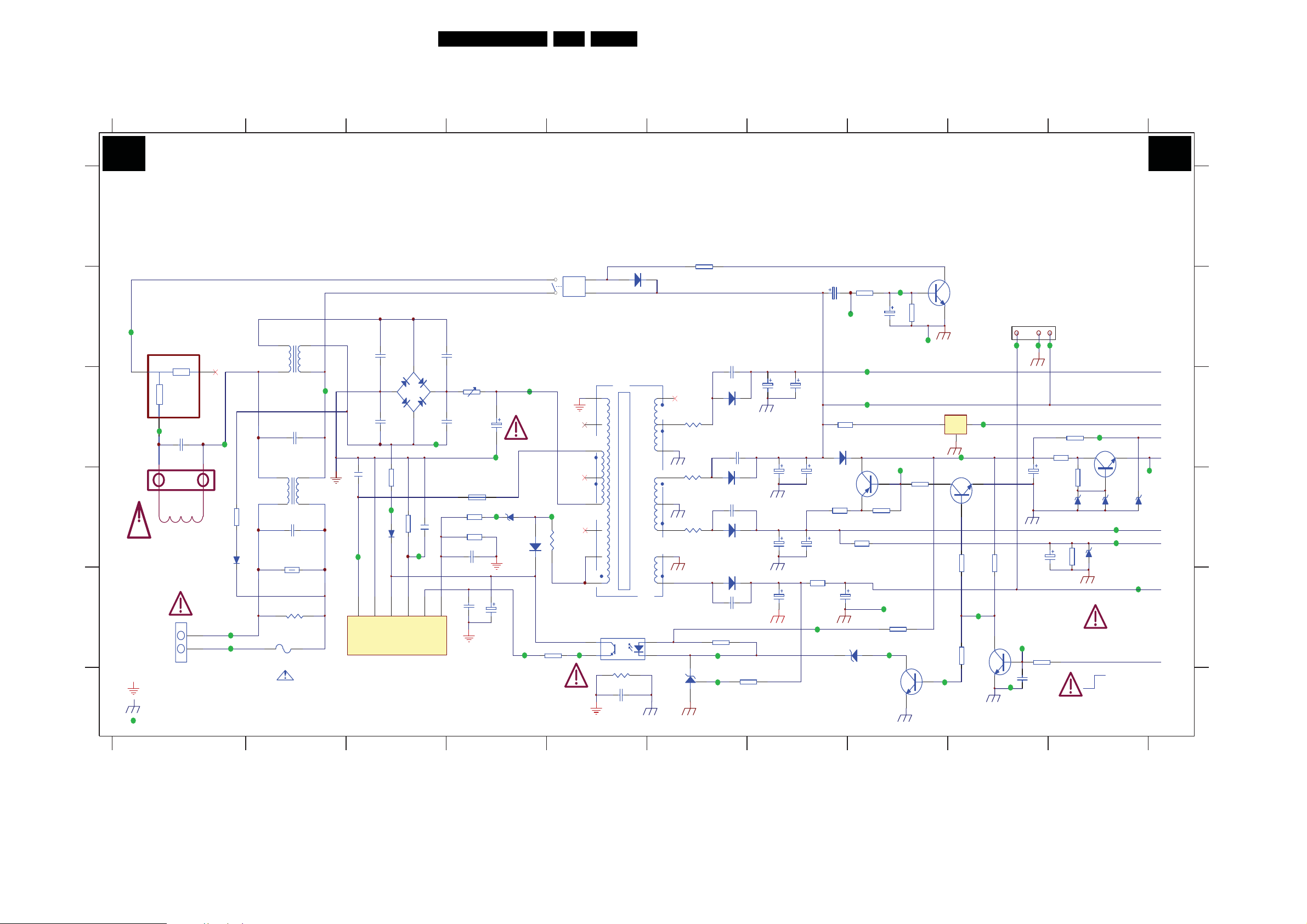
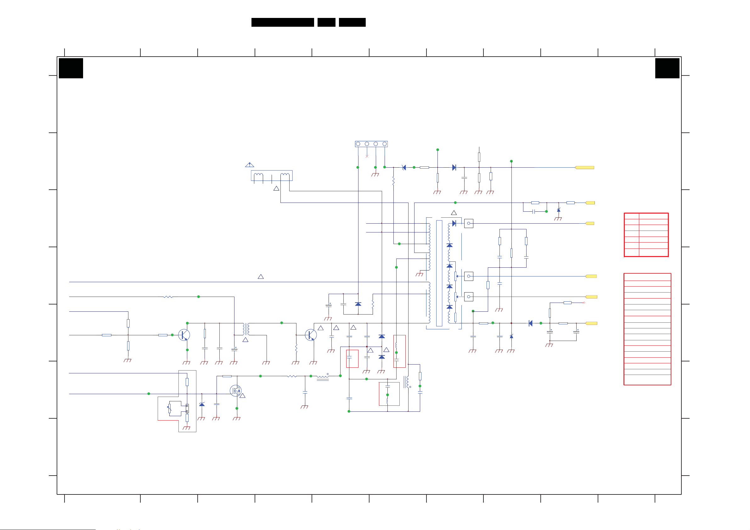
7. Circuit Diagrams and PWB Layouts
Mono Carrier: Power Supply
123 45678 910
11SK5.1L CA 7.
A1 A1
POWER SUPPLY
A
R64 0
R624
0.22 2W
R622
0.22 2W
R62 1
0.22 2W
IC621
SE120
0
680 pF 500V
C623
680 pF 500V
560pF 2KV
R630
680
T630
T631
C624
C620
D623
RU4Y X
680 pF 500V
D622
BYW36
D621
BA158
D620
RU4 B
C46 2
R62 7
6.2K
C62 7
1000uF
25V
C62 5
1000uF
16V
C62 2
470uF
50V
C62 1
100uF
200V
C628
1000uF
25V
C626
1000uF
16V
C62 9
1500uF
50V
R60 9
0.18 5W
T629
C640
220uF
R64 7
0.51 2W
R632
1 2W
T616
D626
BA1 58
250V
C632
47uF
R64 4
10K
R633
5K1
T619
T620
ZD620
5V1
R639
10K
Q624
A1013
T628
T632
C639
47uF
R631
1K
T617
T625
R64 3
47K
R649
2K2
T618
IC104
L7808
+12V
Q621
C1815
T633
Q625
C1815
In Out
Gnd
T622
R635
22K
R634
10K
T640 T641 T642
T621
Q622
C1815
R64 8
22K
T634
Q62 3
C1815
T636
123
T635
R15 4
15K
C634
0.1uF/ 50 V
C64 1
2200uF
4
R638
22
C114
47uF
R645
390
R11 4
39K
R65 0
430
ZD622
3V9
IC103
33V
T623
ZD621
3V9
Q626
C27 03
T626
T627
H:WORKI NG
L:STA N DBY
B
C
D
E
F
PTC601
9RM
T604
2 3
Rp
1
T602
0.1uF/250V
DEG AUSS ING
BLU E
BROWN
(AC FROM KEYBROAD )
HOT G ROUND
COLD GROUND
T***
TEST PA D
Rs
C60 0
CN603
CN604
RL601
RELAY
C604
1000pF
1
D
T607
D604
0
3
S/G ND
C603A
4700pF
D603A
D603D
C60 3D
4700pF
R60 2
39K
4
VCC
IC601
R60 4
39K
T608
5
OLP/SS
L603
25mH
T605
C60 3
T603
R60 3
VDR602
T601
N
2
1
L
T600
0.22uF/2 5 0V
C60 1
0.22uF/ 2 5 0 V
VDR6 01
R60 1
2.2M 1/2W
F60 1
T3.15A
AC250V
L601
25mH
T606
D603B
D603C
C60 5
0.1uF
6
FB
T609
C60 3B
4700pF
R60 0
5NTC
C60 3C
C60 7
4700pF
220uF
450V
L604
R606
6K8
R60 5
220
C60 6
470pF
7
C60 9
10nF
OCP/BD
T610
T611
ZD602
18V
T612
D605
BA1 58
C608
10uF
T614 T615
R60 8
2K2
T613
R60 7
22
STR-W6556A
D627
4148
T603
16 1
15
14
13
12
11
10
TRA NSFORME R
IC622
OPTOISOI
R610 8.2M
C610 0.0022uF
<20V>
2
3
<12V>
4
5
<45V>
6
7
<135V>
89
+21 V
_VCC
+12 V_VCC
+8V_ VCC
+5
V_ VCC
+3.3V_ VCC
T6
24
ZD10
5V1
+48
V_ VCC
+33V_ BT
V_ VCC
+135
T637
STANDBY
I_17880_011.eps
A
B
C
5
D
E
F
270308
123 45
678 910
Circuit Diagrams and PWB Layouts
Mono Carrier: Line Deflection
123 45678 910
12SK5.1L CA 7.
A2 A2
LINE DEFLECTION
A
CN40 1
B
C
D
E
F
+135V_VCC
+48V_VCC
+8V_ VCC
H-out
+8V
EW
R402 0
R401
4K7
R403
NC
T426
R404
100
NTC
R464
560 1W
50K
R406
T421
CN400
T423
T422
R467
33K
R466
39K
Q401
C2482
T420
R405
5K6
2200pF
ZD440
8V2
C402
500V
C403
220pF
500V
R441
56K
C441
0.01uF/50V
CONNECT TO H5 02
1
2
3
4
CN40 2V
6
T411
CN402H
5
T412
T413
!
+16.2V
-16.2V
ZD4 02
R423
6.2 2W
T417
T418
18V
T414
+16.2V
-1 6.2V
HEATER
AFC
FBP
!
B+
L432
790uH
T425
C465
0.47uF
L430
36uH
+180V
C436
560pF
2KV
T431
C435
0.56uF
D433
BA158
!
C432
7n2/2KV
C463
0.39uF/ 400 V
3n9/ 2KV
33nF/630V
T432
C431
!
C433
0.33
1W
D430
BY228
!
D431
RU4B
C464
0.18uF
T433
L431
160uH
FOR SLI M
????
S
C437
10uF
250V
5
4
C404
4.7uF
50V
T427
!
!
Q440
F630
1
T40 1
3
T428
T424
R440
2. 2 2W
R454
33
N401
D2553
T429
C440
4.7uF/ 5 0 V
!
L440 2 .8mH
!
C438
2n7 /2KV
T430
R433
T415
R421
180
R422
680
T402
4
5
8
6
9
3
2
10
1 7
HY
FLYBACK
R432
270
T434
C442
2200PF
D404
4148
T419
!
C407
NC
HV TO CRT
FOCUS
SCRE E N
T436
ABL
+8V_VCC
R413
100K
R418
NC
R420
1K
C443
0.15uF/250V
R408
3.3K
T437
R412
27K
R418
91K
C473
0.1uF
C446
0.1uF
C409
0.1uF
T416
R419
220K
D403
8V2
R407
C444
39pF/5 0V
R471
68K
C472
0.1uF
D402
4148
X-ray
R416
1K
C410A
10uF/ 1 6 V
ZD401
8V2
R424
2K
R409
27K
R417
3K3
22K
T435
T438
SCREE N
+8V_VCC
C410
10uF/ 1 6V
AFC
EHT
FOCUS
ABL
FUNCTIONS
1
2AV2 INPUT
3
4AV OUT
5
6
TONE - CON TRO L
7
FOR RF Tube
R462 1 O HM (2 W)
R417 4. 7K ( 1/6 W)
R419 390K (1/6W)
C463 0 .36uF (400V)
C438 1500pF (2000V)
C431 6800pF (2000V)
C432 6800pF (2000V)
L440 790uH
L430 30uH
R423 5 .6 (2W)
C433 18nF (630V)
R441 75K (1/6W)
R440 6. 8 (2W)
C435 0 OHM
L431 NOT USED
L432 NOT USED
C464 NOT USED
C46 5 NOT USED
AV1 I NP UT
YUV
S-VH S
BTSC
A
B
C
D
E
F
G
FOR SLI M
123 45
I_17880_012.eps
270308
678 910
G
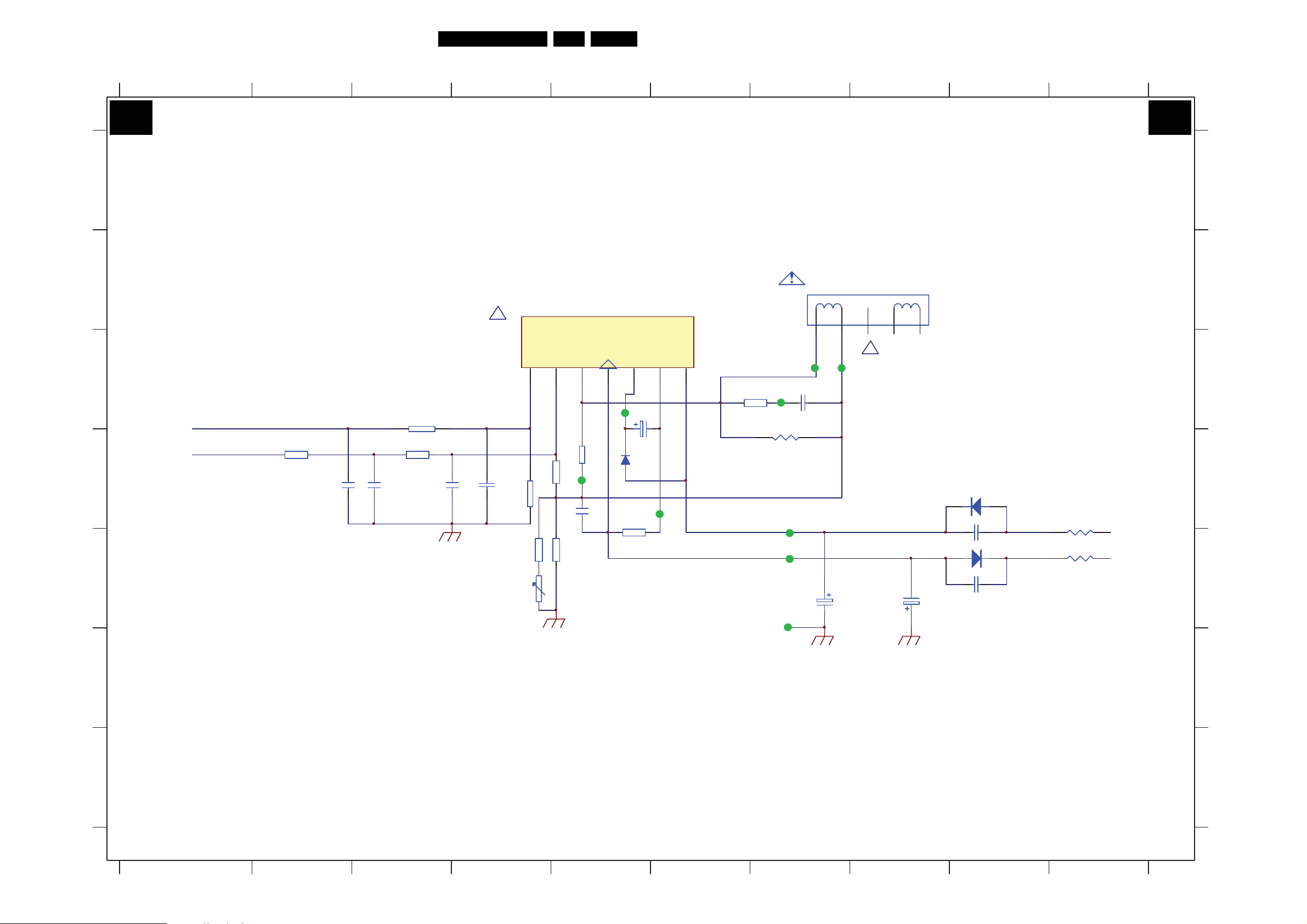
Circuit Diagrams and PWB Layouts
Mono Carrier: Frame Deflection
123 45678 910
13SK5.1L CA 7.
A3 A3
FRAME DEFLECTION
A
B
C
D
E
VD RA
VD RB
R457
100
C160
470P
C161
470P
R460
100
R456
0
1nF/50V
C460
C461
1nF/50V
!
R459
1K8
R426
5.1
R427
5
NTC
IC301
CN40 2V
TDA4865AJ
6
V out
INN
INP
6
35V
J058
1K8
R462
0.82
5
R452
5.6
T400
C459
0. 1uF/ 10 0V
2W
7
4
VP4 -17.5 V
Vp3 pump3VP3-
T401
C455
10 0uF/5 0V
D452
BA158
R463
220 2W
2
T402
VP1 +17.5V
1
R461
5.6 1/4W
T406
T405
0.1uF/10 0V
R45 3
270 1W
T404
T403
C456
5
T407
C453
2200uF/2 5V
!
CN40 2H
+16.2V
-1 6. 2V
2200uF/2 5V
C452
D450
BYW36
470pF
D451
BYW36
470pF
R450
0.22
R451
0.22
2W
2W
+16.2
-16. 2V
A
B
C
D
E
F
G
123 45
T410
I_17880_013.eps
270308
678 910
F
G

Mono Carrier: Tuner IF
123 45678 910
Circuit Diagrams and PWB Layouts
14SK5.1L CA 7.
A4 A4
TUNER IF
A
B
C
D
IDENT RESISTOR
R000
NC
T105
R109
10K
SAS
SCL4SDA5NC
3
T106
R111
R112
100
100
6
C111
100pF
BM +5V
7
8
NC
C113
220uF
9
BT +33 V
IFGND
10IF11
C405
47uF
+5V_VCC
R108
33
ZD101
5V1
AGC
2
1
T104
C112
100pF
R110
180
NC
R113
47K
C109
T333T222
10uF/ 1 6V
C110
A10 1
45.75MHz
C101
0.01uF
R101
75
R103
5.6K
R102
1K2
C103
10nF
NC
R106
1K
NC
Q101
C2717
R105
150
L101
1uH
T107
R107
680
T108
C106
10nF
C105
10nF/50V
C104
100uF
L101
100uH
+8V_ VCC
A
B
C
IF
D
E
F
G
GND
SDA
SCL
CN103
T101
T102
T103
R115 100
R116 100
J002 0
+33 V_ BT
+8V_ VCC
SDA
SCL
AGC
I_17880_014.eps
270308
E
F
G
123 45
678 910
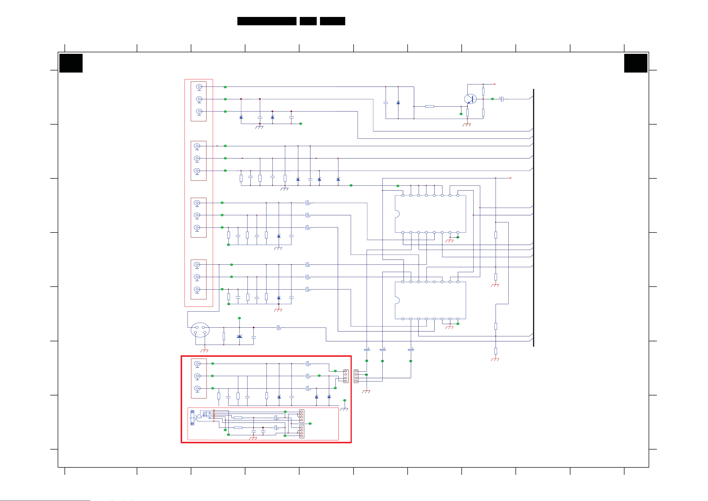
Mono Carrier: AV Switch
123 45678 910
Circuit Diagrams and PWB Layouts
15SK5.1L CA 7.
A5 A5
A
B
C
D
E
F
G
AV SWITCH
P702
S-VHS
P701
V out
L out
R out
AV O UT
Y IN
U IN
V IN
YUV
V IN
L IN
R IN
AV1 I N
V IN
L IN
R IN
AV 2 I N
Y IN
V IN
L IN
R IN
EARP HONE
T701
T702
T703
T707
T708
T709
T711
T712
T713
T714
T717
T718
R703
75
R776
47K
T715
T716
R702
47K
R721
75
ZD704
8V2
C721
R775
C785
47K
R701
C702 C701
47K
T719
ZD707
8V2
C783
C711
C704
R723
75
R719
75
R704
75
SIDE AV BOARD CIRCUIT
T012
T014
T016
R03
47K
R02
C06
2
4
5
3
6
7
1
T025
T026
C04
47K
R02
R04
R01
75
C08
C07
C09C10
ZD703
8V2
C723
ZD712
8V2
ZD706
8V2
C708
10uF/16 V
ZD01
8V2
T027
T023
R722
75
GND
GND
C703
C719
C712
C02
Lo
Ro
Lin
Rin
T706
ZD705
C722
8V2
C778
0.1uF
C770
10uF/16 V
C773
10uF/16V
C707
10uF/16V
C717
10uF/16V
C716
10uF/16V
C01
10uF/16 V
C03
T015
10uF/16 V
C05
10uF/16 V
CN03(TO SPEAKERS)
T024
CN02( FROM CN760)
ZD03
8V2
ZD714
8V2
T013
ZD02
8V2
GND
T018
T017
ZD713
8V2
V
R
L
CN01
VID E O O UT
T710
CN704
+8V
R713
150K
C720
R746
1K5
V OU T
L_AV OUT
R_AV OUT
YUV Y I N
YUV U IN
VUV V IN
+8V
AV1
AV2
TV IN
V OU T
IO1
L OUT
R OUT
C IN
ZD711
C718
8V2
T727
+8V
TV IN
1
+8V
TV IN R
1
C784
C755
1uF/16V
1uF/16V
T723
T725 T726
V
T724
R
L
R717
68
TV
AV1
OUT
SIDE AV
IC761
HCF4052BE
AV2
AV1 V/Y
OUT
SIDE IN
2 3 45678
TV
AV1
OUT
SIDE AV
IC762
HCF4052BE
AV2
AV1 V/Y
OUT
SIDE IN R
2 3 45678
C711
1uF/16V
Q703
C1815
R711
T704
TV2
VSS
TV2
VSS
10K
91011121 3141516
VSS
T722
91011121 3141516
VSS
T722
R712
150K
T705
10uF/16V
R747
1K
R744
15K
R745
4K7
A
B
C
D
E
F
G
123 45
I_17880_015.eps
270308
678 910
 Loading...