

Philips SJA1000-N1, SJA1000T-N1 Datasheet

DATA SH EET
Product specification
Supersedes data of 1999 Aug 17
File under Integrated Circuits, IC18
2000 Jan 04
INTEGRATED CIRCUITS
SJA1000
Stand-alone CAN controller

2000 Jan 04 2
Philips Semiconductors Product specification
Stand-alone CAN controller SJA1000
CONTENTS
1 FEATURES
2 GENERAL DESCRIPTION
3 ORDERING INFORMATION
4 BLOCK DIAGRAM
5 PINNING
6 FUNCTIONAL DESCRIPTION
6.1 Description of the CAN controller blocks
6.1.1 Interface Management Logic (IML)
6.1.2 Transmit Buffer (TXB)
6.1.3 Receive Buffer (RXB, RXFIFO)
6.1.4 Acceptance Filter (ACF)
6.1.5 Bit Stream Processor (BSP)
6.1.6 Bit Timing Logic (BTL)
6.1.7 Error Management Logic (EML)
6.2 Detailed description of the CAN controller
6.2.1 PCA82C200 compatibility
6.2.2 Differences between BasicCAN and PeliCAN
mode
6.3 BasicCAN mode
6.3.1 BasicCAN address layout
6.3.2 Reset values
6.3.3 Control Register (CR)
6.3.4 Command Register (CMR)
6.3.5 Status Register (SR)
6.3.6 Interrupt Register (IR)
6.3.7 Transmit buffer layout
6.3.8 Receive buffer
6.3.9 Acceptance filter
6.4 PeliCAN mode
6.4.1 PeliCAN address layout
6.4.2 Reset values
6.4.3 Mode Register (MOD)
6.4.4 Command Register (CMR)
6.4.5 Status Register (SR)
6.4.6 Interrupt Register (IR)
6.4.7 Interrupt Enable Register (IER)
6.4.8 Arbitration Lost Capture register (ALC)
6.4.9 Error Code Capture register (ECC)
6.4.10 Error Warning Limit Register (EWLR)
6.4.11 RX Error Counter Register (RXERR)
6.4.12 TX Error Counter Register (TXERR)
6.4.13 Transmit buffer
6.4.14 Receive buffer
6.4.15 Acceptance filter
6.4.16 RX Message Counter (RMC)
6.4.17 RX Buffer Start Address register (RBSA)
6.5 Common registers
6.5.1 Bus Timing Register 0 (BTR0)
6.5.2 Bus Timing Register 1 (BTR1)
6.5.3 Output Control Register (OCR)
6.5.4 Clock Divider Register (CDR)
7 LIMITING VALUES
8 THERMAL CHARACTERISTICS
9 DC CHARACTERISTICS
10 AC CHARACTERISTICS
10.1 AC timing diagrams
10.2 Additional AC information
11 PACKAGE OUTLINES
12 SOLDERING
12.1 Introduction
12.2 DIP
12.2.1 Soldering by dipping or by wave
12.2.2 Repairing soldered joints
12.3 SO
12.3.1 Reflow soldering
12.3.2 Wave soldering
12.3.3 Repairing soldered joints
13 DEFINITIONS
14 LIFE SUPPORT APPLICATIONS

2000 Jan 04 3
Philips Semiconductors Product specification
Stand-alone CAN controller SJA1000
1 FEATURES
• Pin compatibility to the PCA82C200 stand-alone CAN
controller
• Electrical compatibility to the PCA82C200 stand-alone
CAN controller
• PCA82C200 mode (BasicCAN mode is default)
• Extended receive buffer (64-byte FIFO)
• CAN 2.0B protocol compatibility (extended frame
passive in PCA82C200 compatibility mode)
• Supports 11-bit identifier as well as 29-bit identifier
• Bit rates up to 1 Mbits/s
• PeliCAN mode extensions:
– Error counters with read/write access
– Programmable error warning limit
– Last error code register
– Error interrupt for each CAN-bus error
– Arbitration lost interrupt with detailed bit position
– Single-shot transmission (no re-transmission)
– Listen only mode (no acknowledge, no active error
flags)
– Hot plugging support (software driven bit rate
detection)
– Acceptance filter extension (4-byte code, 4-byte
mask)
– Reception of‘own’ messages (self reception request)
• 24 MHz clock frequency
• Interfaces to a variety of microprocessors
• Programmable CAN output driver configuration
• Extended ambient temperature range (−40 to +125 °C).
2 GENERAL DESCRIPTION
The SJA1000 is a stand-alone controller for the Controller
Area Network (CAN) used within automotive and general
industrial environments. It is the successor of the
PCA82C200 CAN controller (BasicCAN) from Philips
Semiconductors. Additionally, a new mode of operation is
implemented (PeliCAN) which supports the CAN 2.0B
protocol specification with several new features.
3 ORDERING INFORMATION
TYPE NUMBER
PACKAGE
NAME DESCRIPTION VERSION
SJA1000 DIP28 plastic dual in-line package; 28 leads (600 mil) SOT117-1
SJA1000T SO28 plastic small outline package; 28 leads; body width 7.5 mm SOT136-1
2000 Jan 04 4
Philips Semiconductors Product specification
Stand-alone CAN controller SJA1000
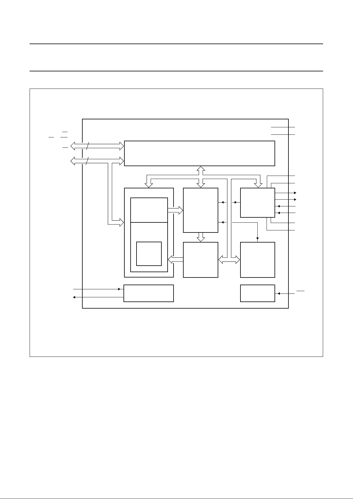
4 BLOCK DIAGRAM
Fig.1 Block diagram.
handbook, full pagewidth
MGK623
INTERFACE MANAGEMENT LOGIC
7
8
address/data
control
MESSAGE BUFFER
TRANSMIT
BUFFER
RECEIVE
BUFFER
RECEIVE
FIFO
BIT
STREAM
PROCESSOR
ACCEPTANCE
FILTER
BIT TIMING
LOGIC
ERROR
MANAGEMENT
LOGIC
RESETOSCILLATOR
XTAL1
9
XTAL2
10
TX0
TX1
RX0
RX1
17
18
21
20
19
14
13
15
12
8
22
internal bus
V
DD3
V
SS3
V
DD1
V
SS1
V
SS2
V
DD2
AD7 to AD0
2, 1,
28 to 23
3 to 7,
11, 16
ALE/AS, CS,
RD/E, WR,
CLKOUT,
MODE, INT
RST
SJA1000

2000 Jan 04 5
Philips Semiconductors Product specification
Stand-alone CAN controller SJA1000
5 PINNING
Note
1. XTAL1 and XTAL2 pins should be connected to V
SS1
via 15 pF capacitors.
SYMBOL PIN DESCRIPTION
AD7 to AD0 2, 1, 28 to 23 multiplexed address/data bus
ALE/AS 3 ALE input signal (Intel mode), AS input signal (Motorola mode)
CS 4 chip select input, LOW level allows access to the SJA1000
RD/E 5 RD signal (Intel mode) or E enable signal (Motorola mode) from the microcontroller
WR 6 WR signal (Intel mode) or RD/WR signal (Motorola mode) from the microcontroller
CLKOUT 7 clock output signal produced by the SJA1000 for the microcontroller; the clock
signal is derived from the built-in oscillator via the programmable divider; the clock
off bit within the clock divider register allows this pin to disable
V
SS1
8 ground for logic circuits
XTAL1 9 input to the oscillator amplifier; external oscillator signal is input via this pin; note 1
XTAL2 10 output from the oscillator amplifier; the output must be left open-circuit when an
external oscillator signal is used; note 1
MODE 11 mode select input
1 = selects Intel mode
0 = selects Motorola mode
V
DD3
12 5 V supply for output driver
TX0 13 output from the CAN output driver 0 to the physical bus line
TX1 14 output from the CAN output driver 1 to the physical bus line
V
SS3
15 ground for output driver
INT 16 interrupt output, used to interrupt the microcontroller; INT is active LOW if any bit of
the internal interrupt register is set; INT is an open-drain output and is designed to
be a wired-OR with other INT outputs within the system; a LOW level on this pin will
reactivate the IC from sleep mode
RST 17 reset input, used to reset the CAN interface (active LOW);automatic power-on reset
can be obtained by connecting RST via a capacitor to VSS and a resistor to V
DD
(e.g. C = 1 µF; R = 50 kΩ)
V
DD2
18 5 V supply for input comparator
RX0, RX1 19, 20 input from the physical CAN-bus line to the input comparator of the SJA1000;
a dominant level will wake up the SJA1000 if sleeping; a dominant level is read, if
RX1 is higher than RX0 and vice versa for the recessive level; if the CBP bit (see
Table 49) is set in the clock divider register, the CAN input comparator is bypassed
to achieve lower internal delays if an external transceiver circuitry is connected to
the SJA1000; in this case only RX0 is active; HIGH is interpreted as recessive level
and LOW is interpreted as dominant level
V
SS2
21 ground for input comparator
V
DD1
22 5 V supply for logic circuits
2000 Jan 04 6
Philips Semiconductors Product specification
Stand-alone CAN controller SJA1000
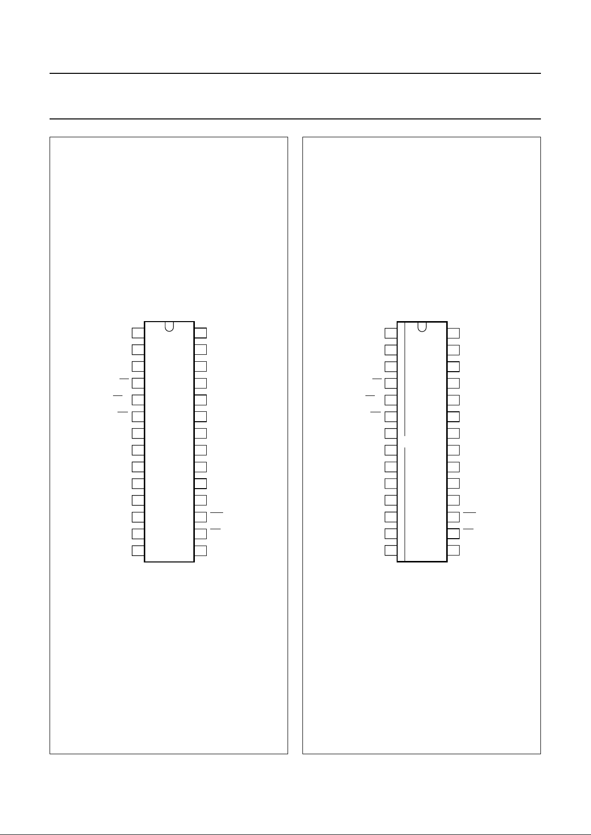
Fig.2 Pin configuration (DIP28).
handbook, halfpage
AD6
AD7
ALE/AS
CLKOUT
V
SS1
XTAL1
XTAL2
MODE
V
DD3
TX0
TX1
AD5
AD4
AD3
AD2
AD0
V
DD1
AD1
V
SS2
RX1
RX0
V
DD2
RST
INT
V
SS3
1
2
3
4
5
6
7
8
9
10
11
12
13
28
27
26
25
24
23
22
21
20
19
18
17
16
1514
SJA1000
MGK616
CS
RD/E
WR
Fig.3 Pin configuration (SO28).
handbook, halfpage
AD6
AD7
ALE/AS
CLKOUT
V
SS1
XTAL1
XTAL2
MODE
V
DD3
TX0
TX1
AD5
AD4
AD3
AD2
AD0
V
DD1
AD1
V
SS2
RX1
RX0
V
DD2
RST
INT
V
SS3
1
2
3
4
5
6
7
8
9
10
11
12
13
28
27
26
25
24
23
22
21
20
19
18
17
16
1514
SJA1000T
MGK617
CS
RD/E
WR

2000 Jan 04 7
Philips Semiconductors Product specification
Stand-alone CAN controller SJA1000
6 FUNCTIONAL DESCRIPTION
6.1 Description of the CAN controller blocks
6.1.1 INTERFACE MANAGEMENT LOGIC (IML)
The interface management logic interprets commands
from the CPU, controls addressing of the CAN registers
and provides interrupts and status information to the host
microcontroller.
6.1.2 TRANSMIT BUFFER (TXB)
The transmit buffer is an interface between the CPU and
the Bit Stream Processor (BSP) that is able to store a
complete message for transmission over the CAN
network. The buffer is 13 bytes long, written to by the CPU
and read out by the BSP.
6.1.3 RECEIVE BUFFER (RXB, RXFIFO)
The receive buffer is an interface between the acceptance
filter and the CPU that stores the received and accepted
messages from the CAN-bus line. The Receive Buffer
(RXB)representsaCPU-accessible13-bytewindowof the
Receive FIFO (RXFIFO), which has a total length of
64 bytes.
With the help of this FIFO the CPU is able to process one
message while other messages are being received.
6.1.4 ACCEPTANCE FILTER (ACF)
Theacceptance filter compares the receivedidentifierwith
the acceptance filter register contents and decides
whether this message should be accepted or not. In the
eventofapositiveacceptancetest, the complete message
is stored in the RXFIFO.
6.1.5 BIT STREAM PROCESSOR (BSP)
Thebitstreamprocessorisasequencerwhichcontrols the
data stream between the transmit buffer, RXFIFO and the
CAN-bus. It also performs the error detection, arbitration,
stuffing and error handling on the CAN-bus.
6.1.6 BIT TIMING LOGIC (BTL)
The bit timing logic monitors the serial CAN-bus line and
handlesthe bus line-related bit timing. It issynchronized to
the bit stream on the CAN-bus on a
‘recessive-to-dominant’bus line transition at the beginning
of a message (hard synchronization) and re-synchronized
on further transitions during the reception of a message
(soft synchronization). The BTL also provides
programmable time segments to compensate for the
propagation delay times and phase shifts (e.g. due to
oscillator drifts) and to define the sample point and the
number of samples to be taken within a bit time.
6.1.7 ERROR MANAGEMENT LOGIC (EML)
The EML is responsible for the error confinement of the
transfer-layer modules. It receives error announcements
from the BSP and then informs the BSP and IML about
error statistics.
6.2 Detailed description of the CAN controller
The SJA1000 is designed to be software and
pin-compatible to its predecessor, the PCA82C200
stand-alone CAN controller. Additionally, a lot of new
functions are implemented. To achieve the software
compatibility, two different modes of operation are
implemented:
• BasicCAN mode; PCA82C200 compatible
• PeliCAN mode; extended features.
The mode of operation is selected with the CAN-mode bit
located within the clock divider register. Default mode
upon reset is the BasicCAN mode.
6.2.1 PCA82C200 COMPATIBILITY
In BasicCAN mode the SJA1000 emulates all known
registers from the PCA82C200 stand-alone CAN
controller. The characteristics, as described in Sections
6.2.1.1 to 6.2.1.4 are different from the PCA82C200
design with respect to software compatibility.
6.2.1.1 Synchronization mode
The SYNC bit in the control register is removed (CR.6 in
the PCA82C200). Synchronization is only possible by a
recessive-to-dominant transition on the CAN-bus. Writing
tothis bit has no effect. Toachieve compatibility to existing
application software, a read access to this bit will reflect
the previously written value (flip-flop without effect).
6.2.1.2 Clock divider register
The clock divider register is used to select the CAN mode
of operation (BasicCAN/PeliCAN). Therefore one of the
reserved bits within the PCA82C200 is used. Writing a
value between 0 and 7, as allowed for the PCA82C200,
will enter the BasicCAN mode. The default state is divide
by 12 for Motorola mode and divide by 2 for Intel mode.
An additionalfunctionis implemented within another of the
reserved bits. Setting of bit CBP (see Table 49) enables
the internal RX input comparator to be bypassed thereby
reducing the internal delays if an external transceiver
circuit is used.

2000 Jan 04 8
Philips Semiconductors Product specification
Stand-alone CAN controller SJA1000
6.2.1.3 Receive buffer
The dual receive buffer concept of the PCA82C200 is
replaced by the receive FIFO from the PeliCAN controller.
Thishasnoeffecttotheapplication software except for the
data overrun probability. Now more than two messages
may be received (up to 64 bytes) until a data overrun
occurs.
6.2.1.4 CAN 2.0B
The SJA1000 is designed to support the full CAN 2.0B
protocol specification, which means that the extended
oscillator tolerance is implemented as well as the
processing of extended frame messages. In BasicCAN
mode it is possible to transmit and receive standard frame
messages only (11-bit identifier). If extended frame
messages (29-bit identifier) are detected on the CAN-bus,
they are tolerated and an acknowledge is given if the
message was correct, but there is no receive interrupt
generated.
6.2.2 DIFFERENCES BETWEEN BASICCAN AND PELICAN
MODE
In the PeliCAN mode the SJA1000 appears with a
re-organized register mapping with a lot of new features.
All known bits from the PCA82C200 design are available
as well as several new ones. In the PeliCAN mode the
complete CAN 2.0B functionality is supported (29-bit
identifier).
Main new features of the SJA1000 are:
• Reception and transmission of standard and extended
frame format messages
• Receive FIFO (64-byte)
• Single/dual acceptance filter with mask and code
register for standard and extended frame
• Error counters with read/write access
• Programmable error warning limit
• Last error code register
• Error interrupt for each CAN-bus error
• Arbitration lost interrupt with detailed bit position
• Single-shot transmission (no re-transmission on error or
arbitration lost)
• Listen only mode (monitoring of the CAN-bus, no
acknowledge, no error flags)
• Hot plugging supported (disturbance-free software
driven bit rate detection)
• Disable CLKOUT by hardware.
6.3 BasicCAN mode
6.3.1 BASICCAN ADDRESS LAYOUT
The SJA1000 appears to a microcontroller as a
memory-mapped I/O device. An independent operation of
both devices is guaranteed by a RAM-like implementation
of the on-chip registers.
The address area of the SJA1000 consists of the control
segment and the message buffers. The control segmentis
programmed during an initialization download in order to
configure communication parameters (e.g. bit timing).
Communication over the CAN-bus is also controlled via
this segment by the microcontroller. During initialization
the CLKOUT signal may be programmed to a value
determined by the microcontroller.
A message, which should be transmitted, has tobe written
to the transmit buffer. After a successful reception the
microcontroller may read the received message from the
receive buffer and then release it for further use.
The exchange of status, control and command signals
between the microcontroller and the SJA1000 is
performed in the control segment. The layout of this
segment is shown in Table 3. After an initial download, the
contents of the registers acceptance code, acceptance
mask, bus timing registers 0 and 1 and output control
should not be changed. Therefore these registers may
only be accessed when the reset request bit in the control
register is set HIGH.
For register access, two different modes have to be
distinguished:
• Reset mode
• Operating mode.
The reset mode (see Table 3, control register, bit Reset
Request) is entered automatically after a hardware reset
or when the controller enters the bus-off state (see
Table 5, status register, bit Bus Status). The operating
modeisactivatedby resetting of the reset request bit in the
control register.

2000 Jan 04 9
Philips Semiconductors Product specification
Stand-alone CAN controller SJA1000
Table 1 BasicCAN address allocation; note 1
Notes
1. It should be noted that the registers are repeated within higher CAN address areas (the most significant bits of the
8-bit CPU address are not decoded: CAN address 32 continues with CAN address 0 and so on).
2. Test register is used for production testing only. Using this register during normal operation may result in undesired
behaviour of the device.
3. Some bits are writeable in reset mode only (CAN mode and CBP).
CAN
ADDRESS
SEGMENT
OPERATING MODE RESET MODE
READ WRITE READ WRITE
0 control control control control control
1 (FFH) command (FFH) command
2 status − status −
3 interrupt − interrupt −
4 (FFH) − acceptance code acceptance code
5 (FFH) − acceptance mask acceptance mask
6 (FFH) − bus timing 0 bus timing 0
7 (FFH) − bus timing 1 bus timing 1
8 (FFH) − output control output control
9 test test; note 2 test test; note 2
10 transmit
buffer
identifier (10 to 3) identifier (10 to 3) (FFH) −
11 identifier (2 to 0),
RTR and DLC
identifier (2 to 0),
RTR and DLC
(FFH) −
12 data byte 1 data byte 1 (FFH) −
13 data byte 2 data byte 2 (FFH) −
14 data byte 3 data byte 3 (FFH) −
15 data byte 4 data byte 4 (FFH) −
16 data byte 5 data byte 5 (FFH) −
17 data byte 6 data byte 6 (FFH) −
18 data byte 7 data byte 7 (FFH) −
19 data byte 8 data byte 8 (FFH) −
20 receive
buffer
identifier (10 to 3) identifier (10 to 3) identifier (10 to 3) identifier (10 to 3)
21 identifier (2 to 0),
RTR and DLC
identifier (2 to 0),
RTR and DLC
identifier (2 to 0),
RTR and DLC
identifier (2 to 0),
RTR and DLC
22 data byte 1 data byte 1 data byte 1 data byte 1
23 data byte 2 data byte 2 data byte 2 data byte 2
24 data byte 3 data byte 3 data byte 3 data byte 3
25 data byte 4 data byte 4 data byte 4 data byte 4
26 data byte 5 data byte 5 data byte 5 data byte 5
27 data byte 6 data byte 6 data byte 6 data byte 6
28 data byte 7 data byte 7 data byte 7 data byte 7
29 data byte 8 data byte 8 data byte 8 data byte 8
30 (FFH) − (FFH) −
31 clock divider clock divider; note 3 clock divider clock divider

2000 Jan 04 10
Philips Semiconductors Product specification
Stand-alone CAN controller SJA1000
6.3.2 RESET VALUES
Detection of a ‘reset request’ results in aborting the current transmission/reception of a message and entering the reset
mode. On the ‘1-to-0’ transition of the reset request bit, the CAN controller returns to the operating mode.
Table 2 Reset mode configuration; notes 1 and 2
REGISTER BIT SYMBOL NAME
VALUE
RESET BY
HARDWARE
SETTING
BIT CR.0 BY
SOFTWAREOR
DUE TO
BUS-OFF
Control CR.7 − reserved 0 0
CR.6 − reserved X X
CR.5 − reserved 1 1
CR.4 OIE Overrun Interrupt Enable X X
CR.3 EIE Error Interrupt Enable X X
CR.2 TIE Transmit Interrupt Enable X X
CR.1 RIE Receive Interrupt Enable X X
CR.0 RR Reset Request 1 (reset mode) 1 (reset mode)
Command CMR.7 − reserved note 3 note 3
CMR.6 − reserved
CMR.5 − reserved
CMR.4 GTS Go To Sleep
CMR.3 CDO Clear Data Overrun
CMR.2 RRB Release Receive Buffer
CMR.1 AT Abort Transmission
CMR.0 TR Transmission Request
Status SR.7 BS Bus Status 0 (bus-on) X
SR.6 ES Error Status 0 (ok) X
SR.5 TS Transmit Status 0 (idle) 0 (idle)
SR.4 RS Receive Status 0 (idle) 0 (idle)
SR.3 TCS Transmission Complete Status 1 (complete) X
SR.2 TBS Transmit Buffer Status 1 (released) 1 (released)
SR.1 DOS Data Overrun Status 0 (absent) 0 (absent)
SR.0 RBS Receive Buffer Status 0 (empty) 0 (empty)
Interrupt IR.7 − reserved 1 1
IR.6 − reserved 1 1
IR.5 − reserved 1 1
IR.4 WUI Wake-Up Interrupt 0 (reset) 0 (reset)
IR.3 DOI Data Overrun Interrupt 0 (reset) 0 (reset)
IR.2 EI Error Interrupt 0 (reset) X; note 4
IR.1 TI Transmit Interrupt 0 (reset) 0 (reset)
IR.0 RI Receive Interrupt 0 (reset) 0 (reset)

2000 Jan 04 11
Philips Semiconductors Product specification
Stand-alone CAN controller SJA1000
Acceptance code AC.7 to 0 AC Acceptance Code X X
Acceptance mask AM.7 to 0 AM Acceptance Mask X X
Bus timing 0 BTR0.7 SJW.1 Synchronization Jump Width 1 X X
BTR0.6 SJW.0 Synchronization Jump Width 0 X X
BTR0.5 BRP.5 Baud Rate Prescaler 5 X X
BTR0.4 BRP.4 Baud Rate Prescaler 4 X X
BTR0.3 BRP.3 Baud Rate Prescaler 3 X X
BTR0.2 BRP.2 Baud Rate Prescaler 2 X X
BTR0.1 BRP.1 Baud Rate Prescaler 1 X X
BTR0.0 BRP.0 Baud Rate Prescaler 0 X X
Bus timing 1 BTR1.7 SAM Sampling X X
BTR1.6 TSEG2.2 Time Segment 2.2 X X
BTR1.5 TSEG2.1 Time Segment 2.1 X X
BTR1.4 TSEG2.0 Time Segment 2.0 X X
BTR1.3 TSEG1.3 Time Segment 1.3 X X
BTR1.2 TSEG1.2 Time Segment 1.2 X X
BTR1.1 TSEG1.1 Time Segment 1.1 X X
BTR1.0 TSEG1.0 Time Segment 1.0 X X
Output control OC.7 OCTP1 Output Control Transistor P1 X X
OC.6 OCTN1 Output Control Transistor N1 X X
OC.5 OCPOL1 Output Control Polarity 1 X X
OC.4 OCTP0 Output Control Transistor P0 X X
OC.3 OCTN0 Output Control Transistor N0 X X
OC.2 OCPOL0 Output Control Polarity 0 X X
OC.1 OCMODE1 Output Control Mode 1 X X
OC.0 OCMODE0 Output Control Mode 0 X X
Transmit buffer − TXB Transmit Buffer X X
Receive buffer − RXB Receive Buffer X; note 5 X; note 5
Clock divider − CDR Clock Divider Register 00000000
(Intel);
00000101
(Motorola)
X
REGISTER BIT SYMBOL NAME
VALUE
RESET BY
HARDWARE
SETTING
BIT CR.0 BY
SOFTWAREOR
DUE TO
BUS-OFF

2000 Jan 04 12
Philips Semiconductors Product specification
Stand-alone CAN controller SJA1000
Notes
1. X means that the value of these registers or bits is not influenced.
2. Remarks in brackets explain functional meaning.
3. Reading the command register will always reflect a binary ‘11111111’.
4. On bus-off the error interrupt is set, if enabled.
5. Internal read/write pointers of the RXFIFO are reset to their initial values. A subsequent read access to the RXB
would show undefined data values (parts of old messages). If a message is transmitted, this message is written in
parallel to the receive buffer but no receive interrupt is generated and the receive buffer area is not locked. So, even
if the receive buffer is empty, the last transmitted message may be read from the receive buffer until it is overridden
by the next received or transmitted message.
Upon a hardware reset, the RXFIFO pointers are reset to the physical RAM address ‘0’. Setting CR.0 by software or
due to the bus-off event will reset the RXFIFO pointers to the currently valid FIFO start address which is different
from the RAM address ‘0’ after the first release receive buffer command.
6.3.3 CONTROL REGISTER (CR)
The contents of the control register are used to change the behaviour of the CAN controller. Bits may be set or reset by
the attached microcontroller which uses the control register as a read/write memory.
Table 3 Bit interpretation of the control register (CR); CAN address 0
BIT SYMBOL NAME VALUE FUNCTION
CR.7 −− −reserved; note 1
CR.6 −− −reserved; note 2
CR.5 −− −reserved; note 3
CR.4 OIE Overrun Interrupt Enable 1 enabled; if the data overrun bit is set, the
microcontroller receives an overrun interrupt
signal (see also status register; Table 5)
0 disabled; the microcontroller receives no overrun
interrupt signal from the SJA1000
CR.3 EIE Error Interrupt Enable 1 enabled; if the error or bus status change, the
microcontroller receives an error interrupt signal
(see also status register; Table 5)
0 disabled; the microcontroller receives no error
interrupt signal from the SJA1000
CR.2 TIE Transmit Interrupt Enable 1 enabled; when a message has been successfully
transmitted or the transmit buffer is accessible
again, (e.g. after an abort transmission command)
the SJA1000 transmits a transmit interrupt signal
to the microcontroller
0 disabled; the microcontroller receives no transmit
interrupt signal from the SJA1000

2000 Jan 04 13
Philips Semiconductors Product specification
Stand-alone CAN controller SJA1000
Notes
1. Any write access to the control register has to set this bit to logic 0 (reset value is logic 0).
2. In the PCA82C200 this bit was used to select the synchronization mode. Because this mode is not longer
implemented, setting this bit has no influence on the microcontroller. Due to software compatibility setting this bit is
allowed. This bit will not change after hardware or software reset. In addition the value written by users software is
reflected.
3. Reading this bit will always reflect a logic 1.
4. During a hardware reset or when the bus status bit is set to logic 1 (bus-off), the reset request bit is set to logic 1
(present). If this bit is accessed by software, a value change will become visible and takes effect first with the next
positiveedge of the internal clock whichoperateswith1⁄2ofthe external oscillator frequency. During anexternalreset
the microcontroller cannot set the reset request bit to logic 0 (absent). Therefore, after having set the reset request
bit to logic 0, the microcontroller must check this bit to ensure that the external reset pin is not being held LOW.
Changes of the reset request bit are synchronized with the internal divided clock. Reading the reset request bit
reflects the synchronized status.
After the reset request bit is set to logic 0 the SJA1000 will wait for:
a) One occurrence of bus-free signal (11 recessive bits), if the preceding reset request has been caused by a
hardware reset or a CPU-initiated reset
b) 128 occurrencesof bus-free, if the preceding resetrequesthas been caused by a CAN controllerinitiated bus-off,
before re-entering the bus-on mode; it should be noted that several registers are modified if the reset request bit
was set (see also Table 2).
6.3.4 COMMAND REGISTER (CMR)
A command bit initiates an action within the transfer layer of the SJA1000. The command register appears to the
microcontroller as a write only memory. If a read access is performed to this address the byte ‘11111111’ is returned.
Between two commands at least one internal clock cycle is needed to process. The internal clock is divided by two from
the external oscillator frequency.
CR.1 RIE Receive Interrupt Enable 1 enabled; when a message has been received
without errors, the SJA1000 transmits a receive
interrupt signal to the microcontroller
0 disabled; the microcontroller receives no transmit
interrupt signal from the SJA1000
CR.0 RR Reset Request; note 4 1 present; detection of a reset request results in
aborting the current transmission/reception of a
message and entering the reset mode
0 absent; on the ‘1-to-0’ transition of the reset
request bit, the SJA1000 returns to the operating
mode
BIT SYMBOL NAME VALUE FUNCTION

2000 Jan 04 14
Philips Semiconductors Product specification
Stand-alone CAN controller SJA1000
Table 4 Bit interpretation of the command register (CMR); CAN address 1
Notes
1. The SJA1000 will enter sleep mode if the sleep bit is set to logic 1 (sleep); there is no bus activity and no interrupt is
pending. Setting of GTS with at least one of the previously mentioned exceptions valid will result in a wake-up
interrupt. After sleep mode is set, the CLKOUT signal continues until at least 15 bit times have passed, to allow a
host microcontroller clocked via this signal to enter its own standby mode before the CLKOUT goes LOW.
The SJA1000 will wake up when one of the three previously mentioned conditions is negated: after ‘Go To Sleep’ is
set LOW (wake-up), there is bus activity or
INT is driven LOW (active). On wake-up, the oscillator is started and a
wake-up interrupt is generated. A sleeping SJA1000 which wakes up due to bus activity will not be able to receive
thismessageuntilit detects 11 consecutive recessive bits (bus-free sequence). It should be noted thatsettingofGTS
isnotpossiblein reset mode. After clearing of reset request, setting ofGTSispossiblefirst, when bus-free is detected
again.
2. This command bit is used to clear the data overrun condition indicated by the data overrun status bit. As long as the
data overrun status bit is set no further data overrun interrupt is generated. It is allowed to give the clear data overrun
command at the same time as a release receive buffer command.
3. After reading the contents of the receive buffer, the microcontroller can release this memory space of the RXFIFO
by setting the release receive buffer bit to logic 1. This may result in another message becoming immediately
available within the receive buffer. This event will force another receive interrupt, if enabled. If there is no other
message available no further receive interrupt is generated and the receive buffer status bit is cleared.
4. The abort transmission bit is used when the CPU requires the suspension of the previously requested transmission,
e.g. to transmit a more urgent message before. A transmission already in progress is not stopped. In order to see if
the original message had been either transmitted successfully or aborted, the transmission complete status bit
should be checked. This should be done after the transmit buffer status bit has been set to logic 1 (released) or a
transmit interrupt has been generated.
5. If the transmission request was set to logic 1 in a previous command, it cannot be cancelled by setting the
transmission request bit to logic 0. The requested transmission may be cancelled by setting the abort transmission
bit to logic 1.
BIT SYMBOL NAME VALUE FUNCTION
CMR.7 −− −reserved
CMR.6 −− −reserved
CMR.5 −− −reserved
CMR.4 GTS Go To Sleep; note 1 1 sleep; the SJA1000 enters sleep mode if no CAN
interrupt is pending and there is no bus activity
0 wake up; SJA1000 operates normal
CMR.3 CDO Clear Data Overrun;
note 2
1 clear; data overrun status bit is cleared
0 no action
CMR.2 RRB Release Receive Buffer;
note 3
1 released; the receive buffer, representing the
message memory space in the RXFIFO is
released
0 no action
CMR.1 AT Abort Transmission;
note 4
1 present; if not already in progress, a pending
transmission request is cancelled
0 absent; no action
CMR.0 TR Transmission Request;
note 5
1 present; a message will be transmitted
0 absent; no action

2000 Jan 04 15
Philips Semiconductors Product specification
Stand-alone CAN controller SJA1000
6.3.5 STATUS REGISTER (SR)
The content of the status register reflects the status of the SJA1000. The status register appears to the microcontroller
as a read only memory.
Table 5 Bit interpretation of the status register (SR); CAN address 2
BIT SYMBOL NAME VALUE FUNCTION
SR.7 BS Bus Status; note 1 1 bus-off; the SJA1000 is not involved in bus
activities
0 bus-on; the SJA1000 is involved in bus activities
SR.6 ES Error Status; note 2 1 error; at least one of the error counters has
reached or exceeded the CPU warning limit
0 ok; both error counters are below the warning limit
SR.5 TS Transmit Status; note 3 1 transmit; the SJA1000 is transmitting a message
0 idle; no transmit message is in progress
SR.4 RS Receive Status; note 3 1 receive; the SJA1000 is receiving a message
0 idle; no receive message is in progress
SR.3 TCS Transmission Complete
Status; note 4
1 complete; the last requested transmission has
been successfully completed
0 incomplete; the previouslyrequestedtransmission
is not yet completed
SR.2 TBS Transmit Buffer Status;
note 5
1 released; the CPU may write a message into the
transmit buffer
0 locked; the CPU cannot access the transmit
buffer; a message is waiting for transmission or is
already in process
SR.1 DOS Data Overrun Status;
note 6
1 overrun; a message was lost because there was
not enough space for that message in the RXFIFO
0 absent; no data overrun has occurred since the
last clear data overrun command was given
SR.0 RBS Receive Buffer Status;
note 7
1 full; one or more messages are available in the
RXFIFO
0 empty; no message is available

2000 Jan 04 16
Philips Semiconductors Product specification
Stand-alone CAN controller SJA1000
Notes
1. When the transmit error counter exceeds the limit of 255 [the bus status bit is set to logic 1 (bus-off)] the
CAN controller will set the reset request bit to logic 1 (present) and an error interrupt is generated, if enabled. It will
stay in this mode until the CPU clears the reset request bit. Once this is completed the CAN controller will wait the
minimum protocol-defined time (128 occurrences of the bus-free signal). After that the bus status bit is cleared
(bus-on), the error status bit is set to logic 0 (ok), the error counters are reset and an error interrupt is generated, if
enabled.
2. Errors detected during reception or transmission will affect the error counters according to the CAN 2.0B protocol
specification. The error status bit is set when at least one of the error counters has reached or exceeded the CPU
warning limit of 96. An error interrupt is generated, if enabled.
3. If both the receive status and the transmit status bits are logic 0 (idle) the CAN-bus is idle.
4. The transmission complete status bit is set to logic 0 (incomplete) whenever the transmission request bit is set to
logic 1. The transmission complete status bit will remain at logic 0 (incomplete) until a message is transmitted
successfully.
5. If the CPU tries to write to the transmit buffer when the transmit buffer status bit is at logic 0 (locked), the written byte
will not be accepted and will be lost without being indicated.
6. When a message that shall be received has passed the acceptance filter successfully (i.e. earliest after arbitration
field), the CAN controller needs space in the RXFIFO to store the message descriptor. Accordingly there must be
enough space for each data byte which has been received. If there is not enough space to store the message, that
message will be dropped and the data overrun condition will be indicated to the CPU only, if this received message
has no errors until the last but one bit of end of frame (message becomes valid).
7. After reading a message stored in the RXFIFO and releasing this memory space with the command release receive
buffer, this bit is cleared. If there is another message available within the FIFO this bit is set again with the next bit
quantum (t
scl
).

2000 Jan 04 17
Philips Semiconductors Product specification
Stand-alone CAN controller SJA1000
6.3.6 INTERRUPT REGISTER (IR)
The interrupt register allows the identification of an interrupt source. When one or more bits of this register are set, the
INT pin is activated (LOW). After this register is read by the microcontroller, all bits are reset what results in a floating
level at INT. The interrupt register appears to the microcontroller as a read only memory.
Table 6 Bit interpretation of the interrupt register (IR); CAN address 3
Notes
1. Reading this bit will always reflect a logic 1.
2. A wake-up interrupt is also generated if the CPU tries to set go to sleep while the CAN controller is involved in bus
activities or a CAN interrupt is pending.
3. The overrun interrupt bit (if enabled) and the data overrun status bit are set at the same time.
4. The receive interrupt bit (if enabled) and the receive buffer status bit are set at the same time.
It should be noted that the receive interrupt bit is cleared upon a read access, even if there is another message
available within the FIFO. The moment the release receive buffer command is given and there is another message
valid within the receive buffer, the receive interrupt is set again (if enabled) with the next t
scl
.
BIT SYMBOL NAME VALUE FUNCTION
IR.7 −− − reserved; note 1
IR.6 −− − reserved; note 1
IR.5 −− − reserved; note 1
IR.4 WUI Wake-Up Interrupt;
note 2
1 set; this bit is set when the sleep mode is left
0 reset; this bit is cleared by any read access of the
microcontroller
IR.3 DOI Data Overrun Interrupt;
note 3
1 set; this bit is set on a ‘0-to-1’ transition of the data
overrun status bit, when the data overrun interrupt
enable is set to logic 1 (enabled)
0 reset; this bit is cleared by any read access of the
microcontroller
IR.2 EI Error Interrupt 1 set; this bit is set on a change of either the error
status or bus status bits if the error interrupt
enable is set to logic 1 (enabled)
0 reset; this bit is cleared by any read access of the
microcontroller
IR.1 TI Transmit Interrupt 1 set; this bit is set whenever the transmit buffer
status changes from logic 0 to logic 1 (released)
and transmit interrupt enable is set to logic 1
(enabled)
0 reset; this bit is cleared by any read access of the
microcontroller
IR.0 RI Receive Interrupt; note 4 1 set; this bit is set while the receive FIFO is not
empty and the receive interrupt enable bit is set
to logic 1 (enabled)
0 reset; this bit is cleared by any read access of the
microcontroller

2000 Jan 04 18
Philips Semiconductors Product specification
Stand-alone CAN controller SJA1000
6.3.7 TRANSMIT BUFFER LAYOUT
Theglobal layout of the transmit buffer is showninTable 7. The buffer serves to store amessagefrom the microcontroller
to be transmitted by the SJA1000. It is subdivided into a descriptor and data field. The transmit buffer can be written to
and read out by the microcontroller in operating mode only. In reset mode a ‘FFH’ is reflected for all bytes.
Table 7 Layout of transmit buffer
CAN
ADDRESS
FIELD NAME
BITS
76543210
10 descriptor identifier byte 1 ID.10 ID.9 ID.8 ID.7 ID.6 ID.5 ID.4 ID.3
11 identifier byte 2 ID.2 ID.1 ID.0 RTR DLC.3 DLC.2 DLC.1 DLC.0
12 data TX data 1 transmit data byte 1
13 TX data 2 transmit data byte 2
14 TX data 3 transmit data byte 3
15 TX data 4 transmit data byte 4
16 TX data 5 transmit data byte 5
17 TX data 6 transmit data byte 6
18 TX data 7 transmit data byte 7
19 TX data 8 transmit data byte 8
6.3.7.1 Identifier (ID)
The identifier consists of 11 bits (ID.10 to ID.0). ID.10 is
themostsignificant bit, which is transmitted first on thebus
during the arbitration process. The identifier acts as the
message’s name. It is used in a receiver for acceptance
filtering and also determining the bus access priority
during the arbitration process. The lower the binary value
of the identifier the higher the priority. This is due to a
larger number of leading dominant bits during arbitration.
6.3.7.2 Remote Transmission Request (RTR)
If this bit is set, a remote frame will be transmitted via the
bus.This means that nodata bytes are included withinthis
frame. Nevertheless, it is necessary to specify the correct
data length code which depends on the corresponding
data frame with the same identifier coding.
If the RTR bit is not set, a data frame will be sent including
the number of data bytes as specified by the data length
code.
6.3.7.3 Data Length Code (DLC)
The number of bytes in the data field of a message is
coded by the data length code. At the start of a remote
frame transmission the data length code is not considered
due to the RTR bit being at logic 1 (remote). This forces
the number of transmitted/received data bytes to be
logic 0. Nevertheless, the data length code must be
specified correctly to avoid bus errors if two
CAN controllersstartaremoteframetransmissionwiththe
same identifier simultaneously.
The range of the data byte count is 0 to 8 bytes and is
coded as follows:
DataByteCount = 8 × DLC.3 + 4 × DLC.2 + 2 × DLC.1 +
DLC.0
Forreasons of compatibility no datalengthcode >8 should
be used. If a value >8 is selected, 8 bytes are transmitted
in the data frame with the data length code specified in
DLC.
6.3.7.4 Data field
The number of transferred data bytes is determined by the
data length code. The first bit transmitted is the most
significant bit of data byte 1 at address 12.
6.3.8 RECEIVE BUFFER
The global layout of the receive buffer is very similar to the
transmit buffer described in Section 6.3.7. The receive
buffer is the accessible part of the RXFIFO and is located
in the range between CAN address 20 and 29.
2000 Jan 04 19
Philips Semiconductors Product specification
Stand-alone CAN controller SJA1000
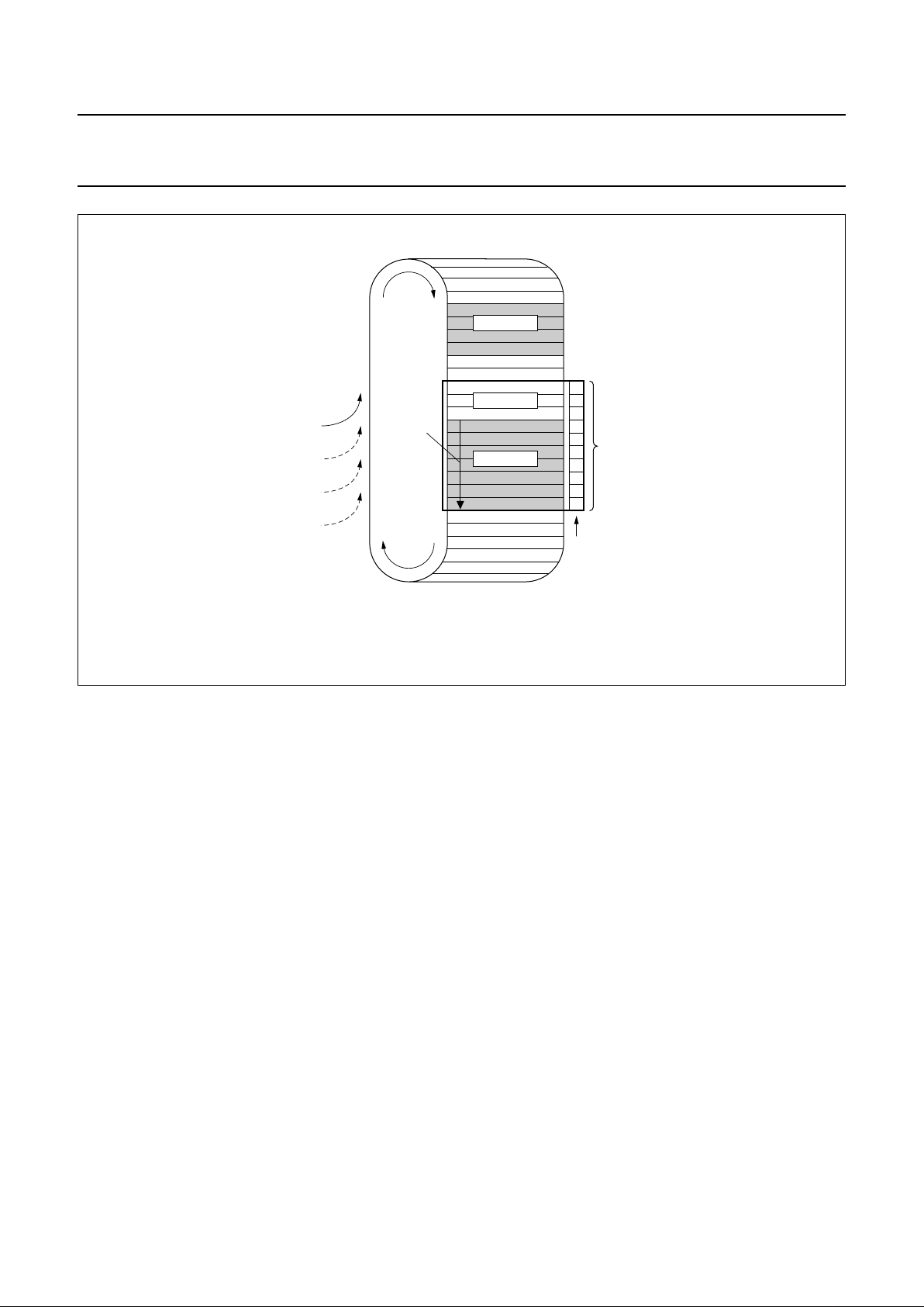
Fig.4 Example of the message storage within the RXFIFO.
Message 1 is now available in the receive buffer.
handbook, full pagewidth
MGK618
release
receive
buffer
command
64-byte
FIFO
incoming
messages
message 3
message 2
message 1
29
28
27
26
25
24
23
22
21
20
receive
buffer
window
CAN address
Identifier, remote transmission request bit and data length
code have the same meaning and location as described in
the transmit buffer but within the address range 20 to 29.
As illustrated in Fig.4 the RXFIFO has space for
64 message bytes in total. The number of messages that
can be stored in the FIFO at any particular moment
depends on the length of the individual messages. If there
is not enough space for a new message within the
RXFIFO, the CAN controller generates a data overrun
condition. A message which is partly written into the
RXFIFO, when the data overrun condition occurs, is
deleted. This situation is indicated to the microcontroller
via the status register and the data overrun interrupt, if
enabled and the frame was received without any errors
until the last but one bit of end of frame (RX message
becomes valid).
6.3.9 ACCEPTANCE FILTER
With the help of the acceptance filter the CAN controller is
abletoallow passing of received messages to the RXFIFO
only when the identifier bits of the received message are
equal to the predefined ones within the acceptance filter
registers. The acceptance filter is defined by the
acceptance code register (ACR; see Section 6.3.9.1) and
the acceptance mask register (AMR; see Section 6.3.9.2).

2000 Jan 04 20
Philips Semiconductors Product specification
Stand-alone CAN controller SJA1000
6.3.9.1 Acceptance Code Register (ACR)
Table 8 ACR bit allocation; can address 4
BIT 7 BIT 6 BIT 5 BIT 4 BIT 3 BIT 2 BIT 1 BIT 0
AC.7 AC.6 AC.5 AC.4 AC.3 AC.2 AC.1 AC.0
This register can be accessed (read/write), if the reset
request bit is set HIGH (present). When a message is
received which passes the acceptance test and there is
receive buffer space left, then the respective descriptor
and data field are sequentially stored in the RXFIFO.
When the complete message has been correctly received
the following occurs:
• The receive status bit is set HIGH (full)
• If the receive interrupt enable bit is set HIGH (enabled),
the receive interrupt is set HIGH (set).
The acceptance code bits (AC.7 to AC.0) and the eight
most significant bits of the message’s identifier
(ID.10 to ID.3) must be equal to those bit positions which
are marked relevant by the acceptance mask bits
(AM.7 to AM.0). If the conditions as described in the
following equation are fulfilled, acceptance is given:
(ID.10 to ID.3) ≡ (AC.7 to AC.0)] ∨ (AM.7 to AM.0)
≡ 11111111
6.3.9.2 Acceptance Mask Register (AMR)
Table 9 AMR bit allocation; CAN address 5
BIT 7 BIT 6 BIT 5 BIT 4 BIT 3 BIT 2 BIT 1 BIT 0
AM.7 AM.6 AM.5 AM.4 AM.3 AM.2 AM.1 AM.0
This register can be accessed (read/write), if the reset
request bit is set HIGH (present). The acceptance mask
register qualifies which of the corresponding bits of the
acceptance code are ‘relevant’ (AM.X = 0) or ‘don’t care’
(AM.X = 1) for acceptance filtering.
6.3.9.3 Other registers
The other registers are described in Section 6.5.
6.4 PeliCAN mode
6.4.1 PELICAN ADDRESS LAYOUT
The CAN controller’s internal registers appear to the CPU
as on-chip memory mapped peripheralregisters. Because
the CAN controller can operate in different modes
(operating/reset; see also Section 6.4.3), one has to
distinguish between different internal address definitions.
Starting from CAN address 32 the complete internal RAM
(80-byte) is mapped to the CPU interface.

2000 Jan 04 21
Philips Semiconductors Product specification
Stand-alone CAN controller SJA1000
Table 10 PeliCAN address allocation; note 1
CAN
ADDRESS
OPERATING MODE RESET MODE
READ WRITE READ WRITE
0 mode mode mode mode
1 (00H) command (00H) command
2 status − status −
3 interrupt − interrupt −
4 interrupt enable interrupt enable interrupt enable interrupt enable
5 reserved (00H) − reserved (00H) −
6 bus timing 0 − bus timing 0 bus timing 0
7 bus timing 1 − bus timing 1 bus timing 1
8 output control − output control output control
9 test test; note 2 test test; note 2
10 reserved (00H) − reserved (00H) −
11 arbitration lost capture − arbitration lost
capture
−
12 error code capture − error code
capture
−
13 error warning limit − error warning
limit
error warning
limit
14 RX error counter − RX error counter RX error counter
15 TX error counter − TX error counter TX error counter
16 RX frame
information
SFF; note 3
RX frame
information
EFF; note 4
TX frame
information
SFF; note 3
TX frame
information
EFF; note 4
acceptance
code 0
acceptance
code 0
17 RX identifier 1 RX identifier 1 TX identifier 1 TX identifier 1 acceptance
code 1
acceptance
code 1
18 RX identifier 2 RX identifier 2 TX identifier 2 TX identifier 2 acceptance
code 2
acceptance
code 2
19 RX data 1 RX identifier 3 TX data 1 TX identifier 3 acceptance
code 3
acceptance
code 3
20 RX data 2 RX identifier 4 TX data 2 TX identifier 4 acceptance
mask 0
acceptance
mask 0
21 RX data 3 RX data 1 TX data 3 TX data 1 acceptance
mask 1
acceptance
mask 1
22 RX data 4 RX data 2 TX data 4 TX data 2 acceptance
mask 2
acceptance
mask 2
23 RX data 5 RX data 3 TX data 5 TX data 3 acceptance
mask 3
acceptance
mask 3
24 RX data 6 RX data 4 TX data 6 TX data 4 reserved (00H) −
25 RX data 7 RX data 5 TX data 7 TX data 5 reserved (00H) −
26 RX data 8 RX data 6 TX data 8 TX data 6 reserved (00H) −
 Loading...