

Philips SDI PDP Repair Manual

Colour Television Module
SDI PDP Repair Manual
S37SD-YD02 (37-inch SD v4)
S42SD-YD05, YD06, YD07 (42-inch SD v2, v3, v4)
S42AX-XD02, YD01 (42-inch HD v3, v4)
S50HW-XD03, XD04 (50-inch HD v3, v4)
Contents Page
1. Technical Specifications, Connections, and Chassis
Overview 2
2. Safety Instructions, Warnings, and Notes 15
3. Directions For Use 16
4. Mechanical Instructions 17
5. Service Modes, Error Codes, and Fault Finding 25
6. Block Diagrams, Test Point Overview, and
Waveforms 40
7. Circuit Diagrams and PWB Layouts 51
8. Alignments 52
9. Circuit Descriptions, Abbreviation List, and IC Data
Sheets 71
10. Spare Parts List 72
11. Revision List 77
©
Copyright 2006 Philips Consumer Electronics B.V. Eindhoven, The Netherlands.
All rights reserved. No part of this publication may be reproduced, stored in a
retrieval system or transmitted, in any form or by any means, electronic,
mechanical, photocopying, or otherwise without the prior permission of Philips.
Published by MW 0663 TV Service Printed in the Netherlands Subject to modification EN 3122 785 14993

EN 2 SDI PDP1.
Technical Specifications, Connections, and Chassis Overview
1. Technical Specifications, Connections, and Chassis Overview
Index of this chapter:
1.1 PDP Overview
1.2 Serial Numbers
1.3 Chassis Overview
Notes:
• Figures can deviate due to the different model executions.
• Specifications are indicative (subject to change).
1.1 PDP Overview
Table 1-1 PDP overview
PDP Type/Version Model Name H x V Pixel
1 37” SD v4 S37SD-YD02 852 x 480
2 42” SD v2 S42SD-YD06 852 x 480
3 42” SD v3 S42SD-YD05 852 x 480
4 42” SD v4 S42SD-YD07 852 x 480
5 42” HD v3 S42AX-XD02 1024 x 768
6 42” HD v4 S42AX-YD01 1024 x 768
7 50” HD v3 S50HW-XD03 1366 x 768
8 50” HD v4 S50HW-XD04 1366 x 768
Table 1-2 PDP vs Chassis overview
Display type Model # Chassis Chassis Manual #
37" SD v4 37PF9936/37 LC4.7U 3122 785 14742
37" SD v4 37PF9946/12 LC4.7E 3122 785 14722
37" SD v4 37PF9946/69 LC4.7A 3122 785 14761
42" SD v2 420P20/00 FM242 3122 785 14130
42" SD v2 42FD9925/01 FM242 3122 785 14130
42" SD v2 42FD9935/17 FM242 3122 785 14130
42" SD v2 42FD9935/93S FM242 3122 785 14130
42" SD v2 42FD9945/01 FM242 3122 785 14130
42" SD v2 42FD9953/17, /69, /93 FM242 3122 785 14130
42" SD v2 42HF9953/12Z FM24_AB 3122 785 13890
42" SD v2 42PF9936/37 FTP1.1U 3122 785 14381
42" SD v2 42PF9945/12 FTP1.1E 3122 785 14370
42" SD v2 42PF9945/69, /79, /98 FTP1.1U 3122 785 14381
42" SD v2 42PF9955/12 F21RE 3122 785 13890
42" SD v3 42PF9936D/37 LC4.7U 3122 785 14742
42" SD v3 42PF9946/12 LC4.7E 3122 785 14722
42" SD v3 42PF9946/79, /93, /98 LC4.7A 3122 785 14761
42" SD v3 42PF9956/12 FTP2.2E 3122 785 14651
42" SD v3 42PF9956/93 FTP2.2A 3122 785 14680
42" SD v4 42PF7320/10 LC4.9E 3122 785 15431
42" SD v4 42PF7320/79, /98 LC4.9A 3122 785 15450
42" HD v3 42PF9966/37 FTP2.2U 3122 785 14662
42" HD v3 42PF9966/79, /93, /98 FTP2.2A 3122 785 14680
42" HD v3 42PF9976/37 FTP2.2U 3122 785 14662
42" HD v4 42HF7543/37 BP2.3HU 3122 785 15900
42" HD v4 42PF7320A/37 BP2.3U 3122 785 15541
42" HD v4 42PF7520D/10 LC4.9E_AB 3122 785 15670
42" HD v4 42PF9630/78 FTP2.4L 3122 785 15470
42" HD v4 42PF9630A/37 BP2.2U 3122 785 15541
42" HD v4 42PF9630A/96 BP2.2U 3122 785 15541
42" HD v4 42PF9966/79, /98 FTP2.4A 3122 785 15470
50" HD v3 50PF9956/37 FTP2.2U 3122 785 14662
50" HD v3 50PF9966/12 FTP2.2E 3122 785 14651
50" HD v3 50PF9966/37 FTP2.2U 3122 785 14662
50" HD v3 50PF9966/69, /93 FTP2.2A 3122 785 14680
50" HD v4 50HF7543/37 BP2.3HU 3122 785 15900
50" HD v4 50PF7320/10 LC4.9E 3122 785 15431
50" HD v4 50PF7320/79, /93, /98 LC4.9A 3122 785 15450
50" HD v4 50PF9630/78 LC4.9L 3122 785 15450
50" HD v4 50PF9630A/96 BP2.2U 3122 785 15541
50" HD v4 50PF9830A/37 BP2.1U 3122 785 15541
50" HD v4 50PF9966/79 FTP2.4A 3122 785 15470
50" HD v4 50PF9967D/10 FTP2.4E_AB 3122 785 15740
In above table the link is given between the SDI Plasma Display
Panel and the Philips TV chassis (incl. chassis manual no.).
1.1.1 37” SD v4
Serial number label
Figure 1-1 External view (37” SD v4)
Figure 1-2 Points of screw mount (37” SD v4)
No Item Specification 37” SD v4
1 Pixel 852 (H) x 480 (V) pixels
2 Number of Cells 2556 (H) x 480 (V)
3 Pixel Pitch 0.960 mm (H) x 0.960 mm (V)
4 Cell Pitch R 0.320 (H) mm
5 Display size 817.92 (H) x 460.80 mm (V)
6 Screen size Diagonal 37" Colour Plasma
7 Screen aspect 16:9
8 Display colour 16.77 million colours
9 Viewing angle Over 160 deg (angle with 50%
10 Dimensions 982 (W) x 582 (H) x 52.9 (D) mm
11 Weight Module 1 About 15.5 kg
12 Broadc. reception
Vertical frequency
Video/Logic Interface
Voltage label Panel module label
F_14991_049.eps
251005
(1 pixel = 1 R,G,B cells)
0.960 (V) mm
G 0.320 (H) mm
0.960 (V) mm
B 0.320 (H) mm
0.960 (V) mm
Display Module
and greater brightness
perpendicular to PDP module)
60/50 Hz, LVDS
Technical Specifications, Connections, and Chassis Overview
EN 3SDI PDP 1.
1.1.2 42" SD v2
Figure 1-3 External view (42” SD v2)
Serial number Model label Voltage label
1.1.3 42" SD v3
Serial number label Model label Voltage label
Figure 1-5 External view (42” SD v3)
This figure is not (yet) available
F_14991_035.eps
061005
Figure 1-4 Points of screw mount (42” SD v2)
No Item Specification 42” SD v2
1 Pixel 852 (H) x 480 (V) pixels
2 Number of Cells 2556 (H) x 480 (V)
3 Pixel Pitch 1.095 mm (H) x 1.110 mm (V)
4 Cell Pitch R 0.324 (H) mm
5 Display size 932.940 (H) x 532.800(V) mm
6 Screen size Diagonal 42" Colour Plasma
7 Screen aspect 16:9
8 Display colour 16.77 million colours
9 Viewing angle Over 160 deg (angle with 50%
10 Dimensions 982 (W) x 582 (H) x 52.9 (D) mm
11 Weight Module 1 About 16.6 kg
12 Broadc. reception
Vertical frequency
Video/Logic Interface
(1 pixel = 1 R,G,B cells)
1.110 (V) mm
G 0.365 (H) mm
1.110 (V) mm
B 0.406 (H) mm
1.110 (V) mm
Display Module
and greater brightness
perpendicular to PDP module)
60/50 Hz, LVDS
Figure 1-6 Points of screw mount (42” SD v3)
No Item Specification 42” SD v3
1 Pixel 852 (H) x 480 (V) pixels
(1 pixel = 1 R,G,B cells)
2 Number of Cells 2556 (H) x 480 (V)
3 Pixel Pitch 1.095 mm (H) x 1.110 mm (V)
4 Cell Pitch R 0.365 (H) mm
1.110 (V) mm
G 0.365 (H) mm
1.110 (V) mm
B 0.365 (H) mm
1.110 (V) mm
5 Display size 932.940 (H) x 532.800(V) mm
6 Screen size Diagonal 42" Colour Plasma
Display Module
7 Screen aspect 16:9
8 Display colour 16.77 million colours
9 Viewing angle Over 160 deg (angle with 50% and
greater brightness perpendicular
to PDP module)
10 Dimensions 982 (W) x 582 (H) x 52.9 (D) mm
11 Weight Module 1 About 16.6 kg
12 Broadc. reception
60/50 Hz, LVDS
Vertical frequency
Video/Logic Interface

EN 4 SDI PDP1.
Technical Specifications, Connections, and Chassis Overview
1.1.4 42" SD v4
Figure 1-7 External view (42” SD v4)
Serial no.
Voltage label
Panel module label
F_14991_003.eps
1.1.5 42" HD v3
Serial number label Panel model labelVoltage label
180705
Figure 1-9 External view (42” HD v3)
F_14991_005.eps
180705
Figure 1-8 Points of screw mount (42” SD v4)
No Item Specification 42” SD v4
1 Pixel 852 (H) x 480 (V) pixels
(1 pixel = 1 R,G,B cells)
2 Number of Cells 2556 (H) x 480 (V)
3 Pixel Pitch 1.095 (H) mm x 1.110 (V) mm
4 Cell Pitch R 0.365 (H) mm x
1.110 (V) mm
G 0.365 (H) mm x
1.110 (V) mm
B 0.365 (H) mm x
1.110 (V) mm
5 Display size 932.940 (H) x 532.800(V) mm
6 Screen size Diagonal 42" Colour Plasma Dis-
play Module
7 Screen aspect 16:9
8 Display colour 16.77 million colours
9 Viewing angle Over 160 deg (angle with 50% and
greater brightness perpendicular
to PDP module)
10 Dimensions 982 (W) x 582 (H) x 54 (D) mm
11 Weight Module 1 About 15.4 kg
14 Broadc. reception
60 Hz/ 50 Hz, LVDS
Vertical frequency
Video/Logic Interface
Figure 1-10 Points of screw mount (42” HD v3)
No Item Specification 42” HD v3
1 Pixel 1.024 (H) x 768 (V) pixels
(1 pixel = 1 R,G,B cells)
2 Number of Cells 3072 (H) x 768 (V)
3 Pixel Pitch 0.912mm (H) x 0.693mm (V)
4 Cell Pitch R Horizontal 0.304 mm
Vertical 0.693 mm
G Horizontal 0.304 mm
Vertical 0.693 mm
B Horizontal 0.304 mm
Vertical 0.693 mm
5 Display size 932.940 (H) x 532.800(V) mm
6 Screen size Diagonal 42" Colour Plasma
Display Module
7 Screen aspect 16:9
8 Display colour 16.77 million colours
9 Viewing angle Over 160 deg (angle with 50% and
greater brightness perpendicular
to PDP module)
10 Dimensions 982 (W) x 582 (H) x 52.9 (D) mm
11 Weight Module 1 About 18.0 kg
12 Broadc. reception
60/50 Hz, LVDS
Vertical frequency
Video/Logic Interface
Technical Specifications, Connections, and Chassis Overview
EN 5SDI PDP 1.
1.1.6 42" HD v4
Figure 1-11 External view (42” HD v4)
F_14991_010.eps
030805
1.1.7 50" HD v3
Serial Number
Figure 1-13 External view (50” HD v3)
Voltage
label
Panel module label
F_14991_011.eps
030805
Figure 1-12 Points of screw mount (42” HD v4)
No Item Specification 42” HD v4
1 Pixel 1.024 (H) x 768 (V) pixels
(1 pixel = 1 R,G,B cells)
2 Number of Cells 3072 (H) x 768 (V)
3 Pixel Pitch 0.912mm (H) x 1.110mm (V)
4 Cell Pitch R Horizontal 0.304 mm
Vertical 0.693 mm
G Horizontal 0.304 mm
Vertical 0.693 mm
B Horizontal 0.304 mm
Vertical 0.693 mm
5 Display size 933.98 (H) x 532.220(V) mm
6 Screen size Diagonal 42" Colour Plasma
Display Module
7 Screen aspect 16:9
8 Display colour 16.77 million colours (8-bit)
9 Viewing angle Over 160 deg (angle with 50% and
greater brightness perpendicular
to PDP module)
10 Dimensions 1000 (W) x 598 (H) x 64.4 (D) mm
11 Weight Module 1 About 20.0 kg
12 Broadc. reception
60/50 Hz, LVDS
Vertical frequency
Video/Logic Interface
Figure 1-14 Points of screw mount (50” HD v3)
No Item Specification 50” HD v3
1 Pixel 1366 (H) x 768 (V) pixels
(1 pixel = 1 R,G,B cells)
2 Number of Cells 4,098 (H) x 768 (V) cells
3 Pixel Pitch 0.810mm (H) mm x 0.810 mm (V)
4 Cell Pitch R Horizontal 0.270mm
Vertical 0.810mm
G Horizontal 0.270mm
Vertical 0.810mm
B Horizontal 0.270mm
Vertical 0.810mm
5 Display size 1106.46 mm (H) x 622.08 mm (H)
6 Screen size Diagonal 50" Colour Plasma
Display Module
7 Screen aspect 16:9
8 Display colour 16.77 million colours
9 Viewing angle Over 160 deg (angle with 50% and
greater brightness perpendicular to
PDP module)
10 Dimensions 1184 (W) x 700 (H) x 60.1 (D) mm
11 Weight Module 1 About 18.0 kg
12 Broadc. reception
60/50 Hz, LVDS
Vertical frequency
Video/Logic Interface
EN 6 SDI PDP1.
Technical Specifications, Connections, and Chassis Overview
1.1.8 50" HD v4
Figure 1-15 External view (50” HD v4)
Serial No.
Volt age label
Panel module label
F_14991_012.eps
030805
1.2 Serial Numbers
ڞڞۇڼێێ ڌڏ ڿۄۂۄۏێ
ڤڟ گ۔ۋۀ
ڤڟ
ڨۀڼۉۄۉۂ
j
Area
ྙ ڜۍۀڼ ڃڞڕ ڞۃۀۊۉڼۉ ڇ ڮ ڕ ڮ ۃۀۉەۀۉڄ
ྚ ڨۊڿۀۇ ڕ ڎ ڿۄۂۄۏ
ྛ ڨۊڿېۇۀ ڧۄۉۀ ڕ ڜ ۙ ڵ
ྜ ڴۀڼۍ ڕ ڌ ڟۄۂۄۏ ژڙ ڭۊۏڼۏۀ ۀۑۀۍ۔ ڿۀھڼڿۀێ
ྜྷ ڨۊۉۏۃ ڃڣۀۓڕ ڌ ڟۄۂۄۏ ژڙ ڪھۏ ڈ ڜ ڇ کۊۑ ڈ ڝڇ ڟۀھ ڈ ڞڄ
ྞ ڟڼۏۀ ڕ ڌ ۙ ڎڌ
ྟ ڲۊۍۆۀۍ ڢۊېۍۋ ڕ ڜ ګڼۍۏڃڟڼ۔ڄڇ ڝ ګڼۍۏڃڜہۏۀۍۉۊۊۉڄڇ ڞ ګڼۍۏڃکۄۂۃۏڄ
2 6 1 4 0 8 07 0 8 6 5
h
WWX
Mod el
[ ` WZ WWWX
Mod ule
Ye ar
Month
Line
Da te
Figure 1-17 Module serial number
h
Worke r
S /N
Gro up
F_14991_004.eps
Serial No : 0001~9999
Date : 01~31
Month : 01~12
Year : 00(2000)
~99(2099)
Line No : 1 ~ 9
(0:Pilot Line)
Type : 02~48
(ex.50HDv3:26)
(Step of even)
180705
F_14991_013.eps
030805
Figure 1-16 Points of screw mount (50” HD v4)
No Item Specification 50” HD v4
1 Pixel 1366 (H) x 768 (V) pixels
(1 pixel = 1 R,G,B cells)
2 Number of Cells 4,098 (H) x 768 (V) cells
3 Pixel Pitch 0.810mm (H) mm x 0.810 mm (V)
4 Cell Pitch R Horizontal 0.270mm
Vertical 0.810mm
G Horizontal 0.270mm
Vertical 0.810mm
B Horizontal 0.270mm
Vertical 0.810mm
5 Display size 1106.46 mm (H) x 622.08 mm (H)
6 Screen size Diagonal 50" Colour Plasma
Display Module
7 Screen aspect 16:9
8 Display colour 16.77 million colours
9 Viewing angle Over 160 deg (angle with 50% and
greater brightness perpendicular
to PDP module)
10 Dimensions 1175 (W) x 682 (H) x 65.5 (D) mm
11 Weight Module 1 About 25.4 kg
12 Broadc. reception
60/50 Hz, LVDS
Vertical frequency
Video/Logic Interface
Figure 1-18 Panel serial number

Technical Specifications, Connections, and Chassis Overview
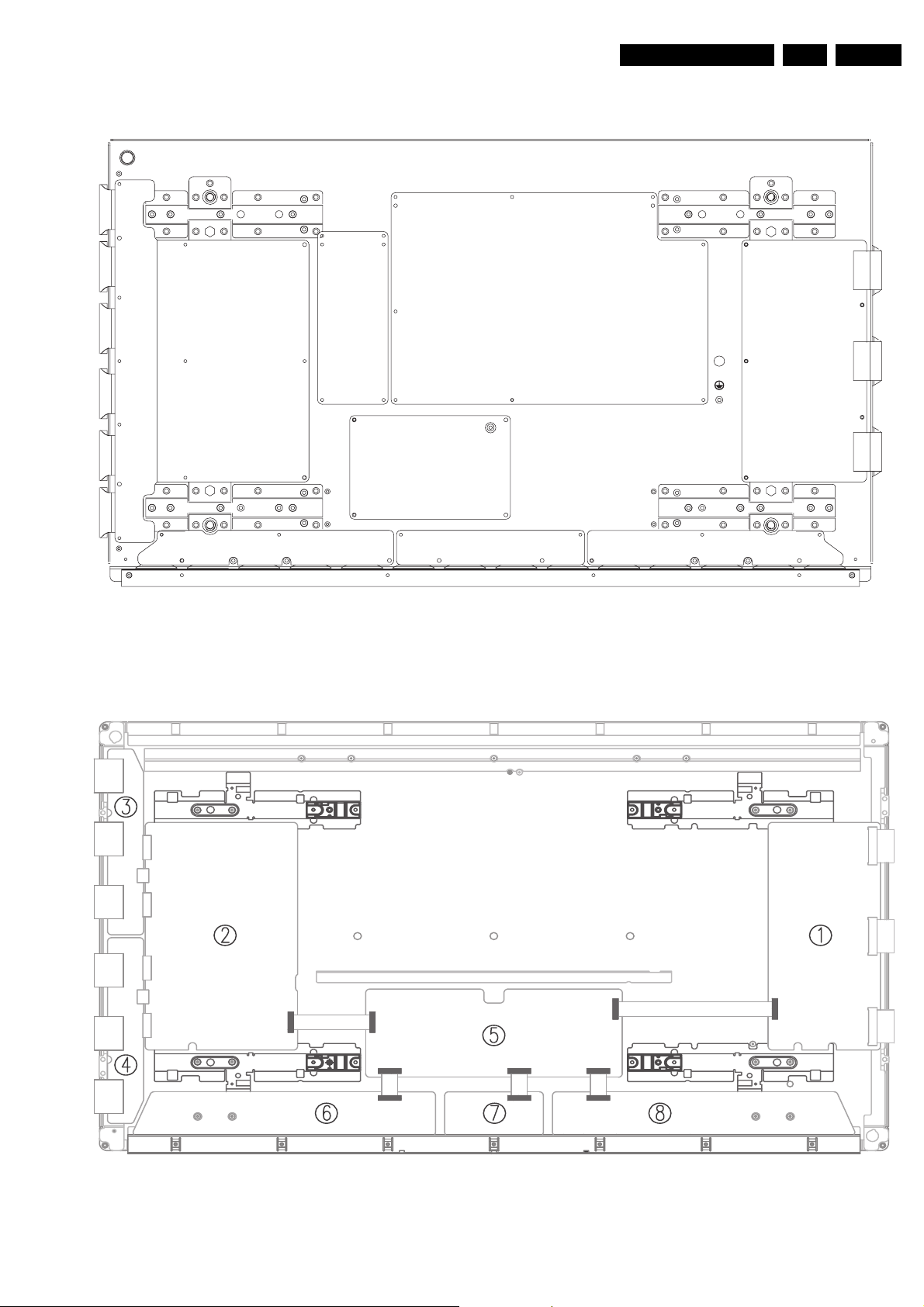
1.3 Chassis Overview
1.3.1 37” SD v4
EN 7SDI PDP 1.
17
9
20
21
1
2
5
19
3
6 7 8
18
12, 13, 14 15, 1610 11
4
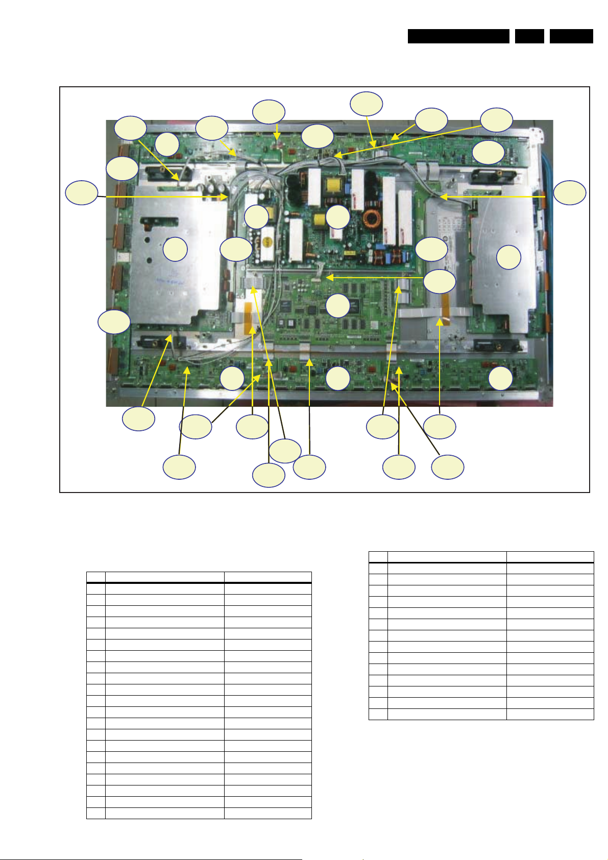
Figure 1-19 PWB location (37” SD v4)
Table 1-3 PWB overview (37” SD v4)
No. Location Name
1 Main PSU Assy PWB PSU
2 SUB-PSU Assy PWB SUB-PSU
3 LOGIC-MAIN Board Assy PWB LOGIC Main
4 X-MAIN Driving Board Assy PWB X Main
5 Y-MAIN Driving Board Assy PWBY Main
6 LOGIC E BUFFER Board Assy PWB Buffer
7 LOGIC F BUFFER Board Assy PWB Buffer
8 LOGIC G BUFFER Board Assy PWB Buffer
9 Y-BUFFER Board Assy PWB Buffer
10 LOGIC + Y-MAIN FFC Cable-flat
11 LOGIC + X-MAIN FFC Cable-flat
12 LOGIC + LOGIC BUF(E) FFC Cable-flat
13 LOGIC + LOGIC BUF(F) FFC Cable-flat
14 LOGIC + LOGIC BUF(G) FFC Cable-flat
15 LOGIC BUF(E) + LOG. BUF(F) Lead connector
16 LOGIC BUF(F) + LOG. BUF(G) Lead connector
17 PSU + SUB PSU Lead connector
18 PSU + LOGIC BUF(E) Lead connector
19 PSU + LOGIC MAIN Lead connector
20 PSU + Y-MAIN Lead connector
F_14991_027.eps
030805

EN 8 SDI PDP1.
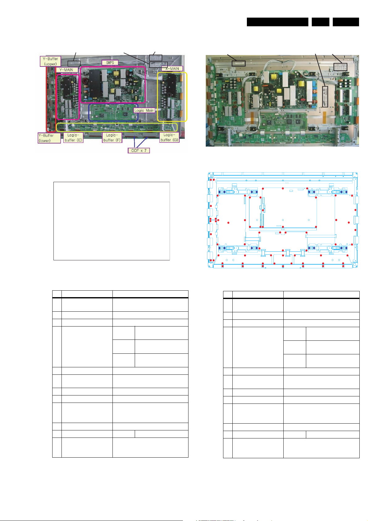
1.3.2 42” SD v2
Y- B uffer
(upper)
Y- MAIN
Technical Specifications, Connections, and Chassis Overview
ڮڨګڮ
X- MAIN
Logic Main
ogic -
Y- B uffer
(lower)
Table 1-4 PWB overview (42” SD v2)
No. Location Name
1 info not available
2
3
4
5
6
7
8
9
10
11
12
13
14
15
16
17
18
19
20
21
22
23
L
buffe r (E )
Logic-
buffe r (F)
Figure 1-20 PWB location (42” SD v2)
C O
F x
Logic
-
buffe r (G)
7
F_14991_033.eps
061005

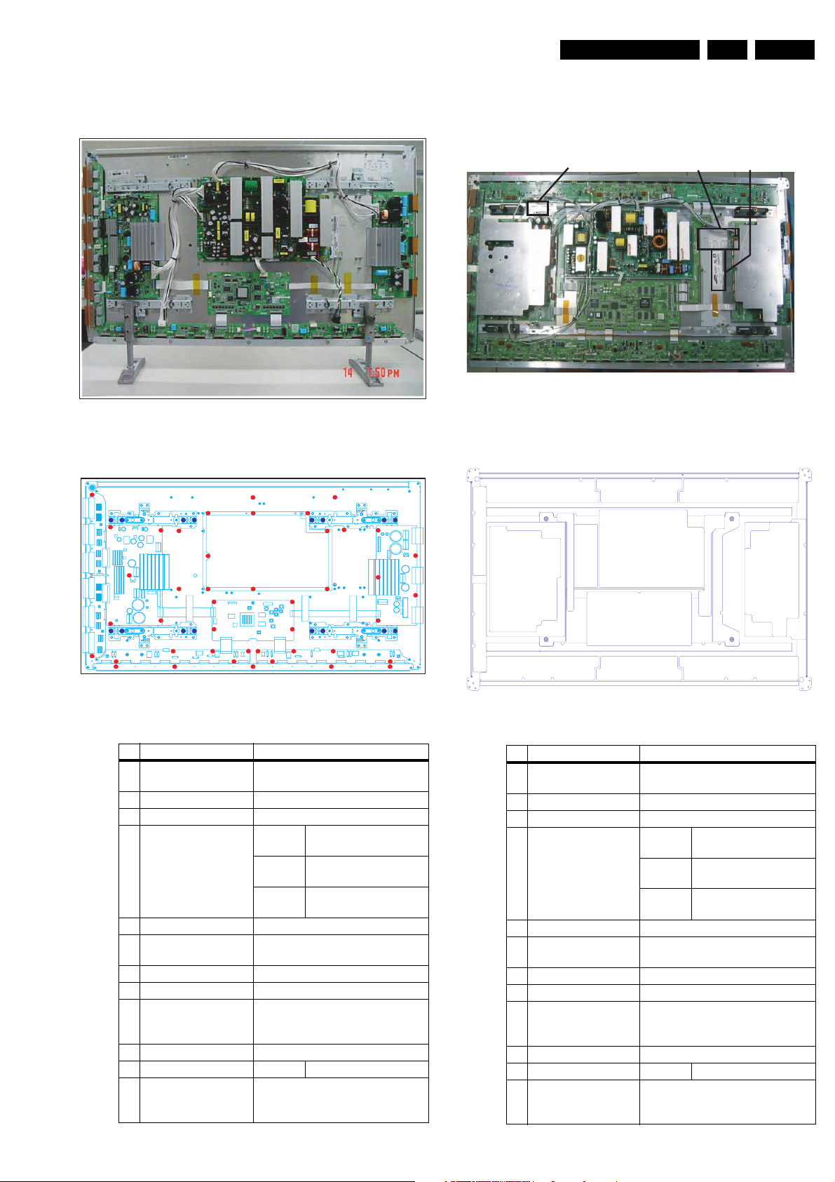
1.3.3 42” SD v3
Technical Specifications, Connections, and Chassis Overview
EN 9SDI PDP 1.
`G
XW
YXG YY
X_G
X
YG
\G
YW
Z
]G ^ _G
XX XY
X`G
GXZSGX[SGX\ X]SGX^
[G
Figure 1-21 PWB location (42” SD v3)
Table 1-5 PWB overview (42” SD v3)
No. Location Name
1 Main PSU Assy PWB PSU
2 SUB-PSU Assy PWB SUB-PSU
3 LOGIC-MAIN Board Assy PWB LOGIC Main
4 X-MAIN Driving Board Assy PWB X Main
5 Y-MAIN Driving Board Assy PWBY Main
6 LOGIC E BUFFER Board Assy PWB Buffer
7 LOGIC F BUFFER Board Assy PWB Buffer
8 LOGIC G BUFFER Board Assy PWB Buffer
9 Y-BUFFER (UPPER) Board Assy PWB Buffer
10 Y-BUFFER (DOWN) Board Assy PWB Buffer
11 LOGIC + Y-MAIN FFC Cable-flat
12 LOGIC + X-MAIN FFC Cable-flat
13 LOGIC + LOGIC BUF(E) FFC Cable-flat
14 LOGIC + LOGIC BUF(F) FFC Cable-flat
15 LOGIC + LOGIC BUF(G) FFC Cable-flat
16 LOGIC BUF(E) +LOG. BUF(F) Lead connector
17 LOGIC BUF(F) +LOG. BUF(G) Lead connector
18 PSU + SUB PSU Lead connector
19 PSU + LOGIC BUF(E) Lead connector
20 PSU + LOGIC MAIN Lead connector
21 PSU + Y-MAIN Lead connector
22 PSU + X-MAIN Lead connector
F_14991_034.eps
061005

EN 10 SDI PDP1.
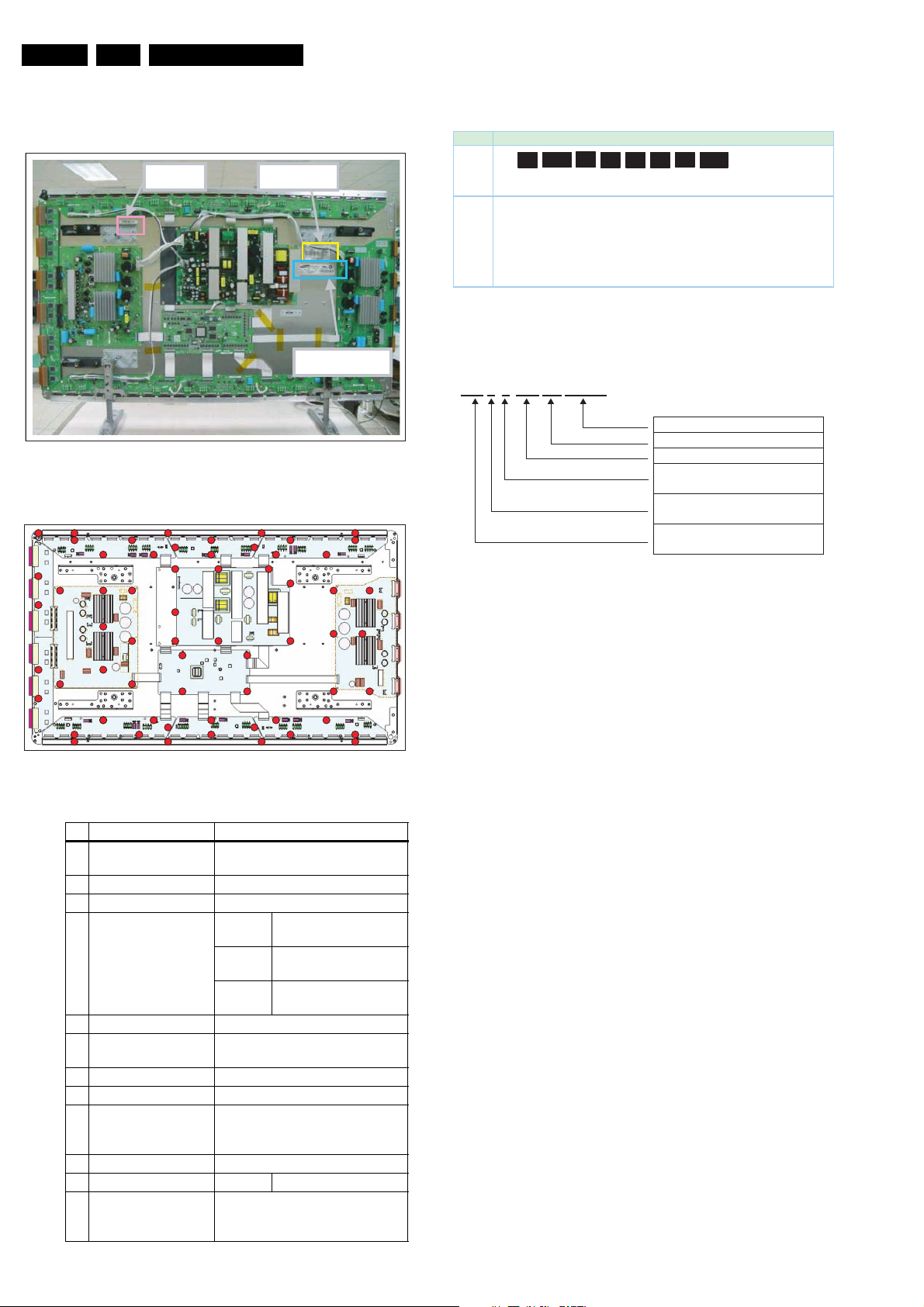
1.3.4 42” SD v4
7
Technical Specifications, Connections, and Chassis Overview
1
16
8
5 6
Figure 1-22 PWB location (42” SD v4)
Table 1-6 PWB overview (42” SD v4)
No. Location Name
1 SMPS SMPS
2 LOGIC-MAIN Board Assy PWB Logic Main
3 X-MAIN Driving Board Assy PWB X Main
4 Y-MAIN Driving Board Assy PWB Y Main
5 LOGIC E BUFFER Board Assy PWB buffer
6 LOGIC F BUFFER Board Assy PWB buffer
7 Y-BUFFER (UPPER) Board Assy PWB buffer
8 Y-BUFFER (DOWN) Board Assy PWB buffer
9 LOGIC + Y-MAIN FFC cable-flat
10 LOGIC + X-MAIN FFC cable-flat
11 LOGIC + LOGIC BUF (E) FFC cable-flat
12 LOGIC + LOGIC BUF (F) FFC cable-flat
13 LOGIC BUF (E) + (F) Lead connector
14 SMPS + LOGIC BUF (E) Lead connector
15 SMPS + LOGIC MAIN Lead connector
16 SMPS + Y-MAIN Lead connector
17 SMPS + X-MAIN Lead connector
3
174
2
15
10 9 11 121314
F_14991_001.eps
180705
1.3.5 42” HD v3
Technical Specifications, Connections, and Chassis Overview
EN 11SDI PDP 1.
8
9
5
18 21
14 15
1
2
4
20
17
3
20
11
22
6
7
10
19
13
Figure 1-23 PWB location (42” HD v3)
Table 1-7 PWB overview (42” HD v3)
No. Location Name
1 Main PSU Assy PWB PSU
2 SUB-PSU Assy PWB SUB-PSU
3 LOGIC-MAIN Board Assy PWB LOGIC Main
4 X-MAIN Driving Board Assy PWB X Main
5 Y-MAIN Driving Board Assy PWB Y Main
6 LOGIC E BUFFER Board Assy PWB Buffer
7 LOGIC F BUFFER Board Assy PWB Buffer
8 Y-BUFFER (UPPER) Board Assy PWB BuffeR
9 Y-BUFFER (DOWN) Board Assy PWB Buffer
10 LOGIC + Y-MAIN FFC Cable-flat
11 LOGIC + X-MAIN FFC Cable-flat
12 LOGIC + LOG. BUF(E) (Down) FFC Cable-flat
13 LOGIC + LOG. BUF(F) (Down) FFC Cable-flat
14 LOGIC + LOGIC BUF(E) (Up) FFC Cable-flat
15 LOGIC + LOGIC BUF(E) (Up) FFC Cable-flat
16 LOGIC BUF(E) + LOG. BUF(F) Lead connector
17 PSU + SUB PSU Lead connector
18 PSU + LOGIC BUF(E) (UP) Lead connector
19 PSU + LOGIC BUF(E) (Down) Lead connector
20 PSU + LOGIC MAIN Lead connector
21 PSU + Y-MAIN Lead connector
22 PSU + X-MAIN Lead connector
12
16
F_14991_014.eps
030805

EN 12 SDI PDP1.
1.3.6 42” HD v4
Technical Specifications, Connections, and Chassis Overview
Y
Figure 1-24 PWB location (42” HD v4)
Table 1-8 PWB overview (42” HD v4)
No. Location Name
1 SMPS SMPS
2 LOGIC-MAIN Board Assy PWBLOGIC Main
3 X-MAIN Driving Board Assy PWBX Main
4 Y-MAIN Driving Board Assy PCBY Main
5 LOGIC E BUFFER Board Assy PWB Buffer
6 LOGIC F BUFFER Board Assy PWB Buffer
7 Y-BUFFER (UPPER) Board Assy PWB Buffer
8 Y-BUFFER (DOWN) Board Assy PWB Buffer
9 LOGIC + Y-MAIN FFC Cable-flat
10 LOGIC + X-MAIN FFC Cable-flat
11 LOGIC + LOGIC BUF(E) FFC Cable-flat
12 LOGIC + LOGIC BUF(F) FFC Cable-flat
13 LOGIC BUF(E) + LOG. BUF(F) Lead connector
14 SMPS + LOGIC BUF(E) Lead connector
15 SMPS + LOGIC MAIN Lead connector
16 SMPS + Y-MAIN Lead connector
17 SMPS + X-MAIN Lead connector
F_14991_015.eps
030805
1.3.7 50” HD v3
Technical Specifications, Connections, and Chassis Overview
EN 13SDI PDP 1.
20
27
35
11
28 32
9
26
10
12
33 34
2 1
5 14 15
4
30
3
13
6 7 8
29
24
16
19
31 23 25
Table 1-9 PWB overview (50” HD v3)
No. Location Name
1 Main PUS Assy PWBPSU
2 SUB-PSU Assy PWBSUB-PSU
3 LOGIC-MAIN Board Assy PWBLOGIC Main
4 X-MAIN Driving Board Assy PWBX Main
5 Y-MAIN Driving Board Assy PCBY Main
6 LOGIC E BUFFER Board Assy PWB Buffer
7 LOGIC F BUFFER Board Assy PWB Buffer
8 LOGIC G BUFFER Board Assy PWB Buffer
9 LOGIC H BUFFER Board Assy PWB Buffer
10 LOGIC I BUFFER Board Assy PWB Buffer
11 LOGIC J BUFFER Board Assy PWB Buffer
12 Y-BUFFER (UPPER) Board Assy PWB Buffer
13 Y-BUFFER (DOWN) Board Assy PWB Buffer
14 SUB-R Assy PWB Buffer
15 SUB-L Assy PWB Buffer
16 LOGIC + Y-MAIN FFC Cable-flat
17 LOGIC + X-MAIN FFC Cable-flat
18 SUB R + LOGIC FFC Cable-flat
19 SUB L + LOGIC FFC Cable-flat
20 LOG.BUF(I) + LOG.BUF(J) (Up) FFC Cable-flat
21 LOGIC + LOG. BUF(E) (Down) FFC Cable-flat
21
Figure 1-25 PWB location (50” HD v3)
18 17
22
F_14991_016.eps
030805
No. Location Name
22 LOGIC + LOG. BUF(F) (Down) FFC Cable-flat
23 LOGIC + LOG. BUF(G) (Down) FFC Cable-flat
24 LOGIC BUF(E) + LOG. BUF(F) Lead connector
25 LOGIC BUF(F) + LOG. BUF(G) Lead connector
26 LOGIC BUF(H) + LOG. BUF(I) Lead connector
27 LOGIC BUF(I) + LOG. BUF(J) Lead connector
28 Y-MAIN + LOGIC BUF(H) Lead connector
29 Y-MAIN + LOGIC BUF(E) Lead connector
30 PSU + LOGIC MAIN Lead connector
31 PSU + LOGIC BUF(E) Lead connector
32 PSU + LOGIC BUF(H) Lead connector
33 PSU + Y-MAIN Lead connector
34 PSU + X-MAIN Lead connector
35 PSU + SUB PSU Lead connector

EN 14 SDI PDP1.
1.3.8 50” HD v4
Technical Specifications, Connections, and Chassis Overview
8
9
20
7
5
4
21
15 16
6
23
2
19
6
1918
17
7
1
24
3
22
18
5
10 12 14
Figure 1-26 PWB location (50” HD v4)
Table 1-10 PWB overview (50” HD v4)
No. Location Name
1 SMPS SMPS
2 LOGIC-MAIN Board Assy PWBLOGIC Main
3 X-MAIN Driving Board Assy PWBX Main
4 Y-MAIN Driving Board Assy PCBY Main
5 LOGIC E BUFFER Board Assy PWB Buffer
6 LOGIC F BUFFER Board Assy PWB Buffer
7 LOGIC G BUFFER Board Assy PWB Buffer
8 Y-BUFFER (Upper) Board Assy PWB Buffer
9 Y-BUFFER (Down) Board Assy PWB Buffer
10 LOGIC + Y-MAIN FFC Cable-flat
11 LOGIC + X-MAIN FFC Cable-flat
12 LOGIC + LOG. BUF(G: Down) FFC Cable-flat
13 LOGIC + LOG. BUF(F: Down) FFC Cable-flat
14 LOGIC + LOG. BUF(E: Down) FFC Cable-flat
15 LOGIC + LOG. BUF(E: Upper) FFC Cable-flat
16 LOGIC + LOG. BUF(F: Upper) FFC Cable-flat
17 LOGIC + LOG. BUF(G: Upper) FFC Cable-flat
18 LOGIC BUF(E) + LOG. BUF(F) Lead connector
19 LOGIC BUF(F) + LOG. BUF(G) Lead connector
20 SMPS + LOGIC BUF(G: Down) Lead connector
21 SMPS + LOGIC BUF(E: Upper) Lead connector
22 SMPS + LOGIC MAIN Lead connector
23 SMPS + Y-MAIN Lead connector
24 SMPS + X-MAIN Lead connector
13
11
F_14991_017.eps
030805

Safety Instructions, Warnings, and Notes
2. Safety Instructions, Warnings, and Notes
EN 15SDI PDP 2.
Index of this chapter:
2.1 Handling Precautions
2.2 Safety Precautions
2.3 Notes
Notes:
• Only authorised persons should perform servicing of this
module.
• When using/handling this unit, pay special attention to the
PDP Module: it should not be enforced into any other way
then next rules, warnings, and/or cautions.
• "Warning" indicates a hazard that may lead to death or
injury if the warning is ignored and the product is handled
incorrectly.
• "Caution" indicates a hazard that can lead to injury or
damage to property if the caution is ignored and the
product is handled incorrectly.
2.1 Handling Precautions
• The PDP module use high voltage that is dangerous to
humans. Before operating the PDP, always check for dust
to prevent short circuits. Be careful touching the circuit
device when power is “on”.
• The PDP module is sensitive to dust and humidity.
Therefore, assembling and disassembling must be done in
no dust place.
• The PDP module has a lot of electric devices. The service
engineer must wear equipment (for example, earth ring) to
prevent electric shock and working clothes to prevent
electrostatic.
• The PDP module use a fine pitch connector which is only
working by exactly connecting with flat cable. The operator
must pay attention to a complete connection when
connector is reconnected after repairing.
• The capacitor’s remaining voltage in the PDP module’s
circuit board temporarily remains after power is “off”.
Operator must wait for discharging of remaining voltage
during at least 1 minute.
2.2 Safety Precautions
2.2.1 Safety Precautions
parts and circuit board. Check the cord of AC power
preparing damage.
• Product Safety Mark: Some of electric or implement
material have special characteristics invisible that was
related on safety. In case of the parts are changed with new
one, even though the Voltage and Watt is higher than
before, the Safety and Protection function will be lost.
• The AC power always should be turned “off”, before next
repair.
• Check assembly condition of screw, parts and wire
arrangement after repairing. Check whether the material
around the parts get damaged.
2.2.2 ESD Precautions
There are parts, which are easily damaged by electrostatics
(for example Integrated Circuits, FETs, etc.) Electrostatic
damage rate of product will be reduced by the following
technics:
• Before handling semiconductor parts/assembly, must
remove positive electric by ground connection, or must
wear the antistatic wrist-belt and ring (it must be operated
after removing dust on it. It comes under precaution of
electric shock).
• After removing the assembly, lay it with the tracks on a
conductive surface to prevent charging.
• Do not use chemical stuff containing Freon. It generates
positive electric that can damage ESD sensitive devices.
• You must use a soldering device for ground-tip when
soldering or de-soldering these devices.
• You must use anti-static solder removal device. Most
removal devices do not have antistatic which can charge a
enough positive electric enough for damaging these
devices.
• Before removing the protective material from the lead of a
new device, bring the protective material into contact with
the chassis or assembly.
• When handing an unpacked device for replacement, do not
move around too much. Moving (legs on the carpet, for
example) generates enough electrostatic to damage the
device.
• Do not take a new device from the protective case until the
it is ready to be installed. Most devices have a lead, which
is easily short-circuited by conductive materials (such as
conductive foam and aluminium)
• Before replacing a board, discharge forcibly.
• The remaining electricity from board.
• When connecting FFC and TCPs to the module, recheck
that they are perfectly connected.
• To prevent electrical shock, be careful not to touch leads
during circuit operations.
• To prevent the Logic circuit from being damaged due to
wrong working, do not connect/disconnect signal cables
during circuit operations.
• Do thoroughly adjustment of a voltage label and voltageinsulation.
• Before reinstalling the chassis and the chassis assembly,
be sure to use all protective stuff including a nonmetal
controlling handle and the covering of partitioning type.
• Caution for design change: Do not install any additional
devices to the module, and do not change the electrical
circuit design.
• For example: Do not insert a subsidiary audio or video
connector. If you insert It, it cause danger on safety. And, if
you change the design or insert, manufacturer guarantee
will be not effect.
• If any parts of wire is overheats of damaged, replace it with
a new specified one immediately, and identify the cause of
the problem and remove the possible dangerous factors.
• Examine carefully the cable status if it is twisted or
damaged or displaced. Do not change the space between
2.3 Notes
A glass plate is positioned before the plasma display. This
glass plate can be cleaned with a slightly humid cloth. If due to
circumstances there is some dirt between the glass plate and
the plasma display panel, it is recommended to do some
maintenance by a qualified service employee only.
2.3.1 Safe PDP Handling
• The work procedures shown with the “Note” indication are
important for ensuring the safety of the product and the
servicing work. Be sure to follow these instructions.
• Before starting the work, secure a sufficient working space.
• At all times, other than when adjusting and checking the
product, be sure to turn “off” the main POWER switch and
disconnect the power cable from the power source of the
display (jig or the display itself) during servicing.
• To prevent electric shock and breakage of PWBs, start the
servicing work at least 30 seconds after the main power
has been turned “off”. Especially when installing and
removing the Power Supply PWB and the SUS PWB in
which high voltages are applied, start servicing at least 2
minutes after the main power has been turned “off”.

EN 16 SDI PDP3.
Directions For Use
• While the main power is “on”, do not touch any parts or
circuits other than the ones specified. The high voltage
Power Supply block within the PDP module has a floating
ground. If any connection other than the one specified is
made between the measuring equipment and the high
voltage power supply block, it can result in electric shock or
activation of the leakage-detection circuit breaker.
• When installing the PDP module in, and removing it from
the packing carton, be sure to have at least two persons
perform the work while being careful to ensure that the
flexible printed-circuit cable of the PDP module does not
get caught by the packing carton.
• When the surface of the panel comes into contact with the
cushioning materials, be sure to confirm that there is no
foreign matter on top of the cushioning materials before the
surface of the panel comes into contact with the cushioning
materials. Failure to observe this precaution may result in,
the surface of the panel being scratched by foreign matter.
• When handling the circuit PWB, be sure to remove static
electricity from your body before handling the circuit PWB.
• Be sure to handle the circuit PWB by holding the large parts
as the heat sink or transformer. Failure to observe this
3. Directions For Use
Not applicable.
precaution may result in the occurrence of an abnormality
in the soldered areas.
• Do not stack the circuit PWB. Failure to observe this
precaution may result in problems resulting from scratches
on the parts, the deformation of parts, and short-circuits
due to residual electric charge.
• Routing of the wires and fixing them in position must be
done in accordance with the original routing and fixing
configuration when servicing is completed. All the wires are
routed far away from the areas that become hot (such as
the heat sink). These wires are fixed in position with the
wire clamps so that the wires do not move, thereby
ensuring that they are not damaged and their materials do
not deteriorate over long periods of time. Therefore, route
the cables and fix the cables to the original position and
states using the wire clamps.
• Perform a safety check when servicing is completed. Verify
that the peripherals of the serviced points have not
undergone any deterioration during servicing. Also verify
that the screws, parts and cables removed for servicing
purposes have all been returned to their proper locations in
accordance with the original

4. Mechanical Instructions
Index of this chapter:
4.1 Dis-assembling / Re-assembling
4.1.1 Flexible Printed Circuit of Y-Buffer (Upper and Lower)
4.1.2 Flat Cable Connector of X-main Board
4.1.3 FFC and TCP from Connector
4.1.4 Exchange of LBE, LBF, LBG board
4.1.5 Exchange YBU, YBL and YM board
4.1 Dis-assembling / Re-assembling
4.1.1 Flexible Printed Circuit of Y-Buffer (Upper and Lower)
• Dis-assembly: Pull out the FPC from the connector by
holding the lead of the FPC with both hands.
• Re-assembly: Push the lead of FPC with same force on
both sides into the connector.
Note: Be careful do not to damage the connector pin
during connecting.
Mechanical Instructions
EN 17SDI PDP 4.
Figure 4-1 Dis-assembly FPC of Y-buffer
Figure 4-2 Re-assembly FPC of Y-buffer
EN 18 SDI PDP4.
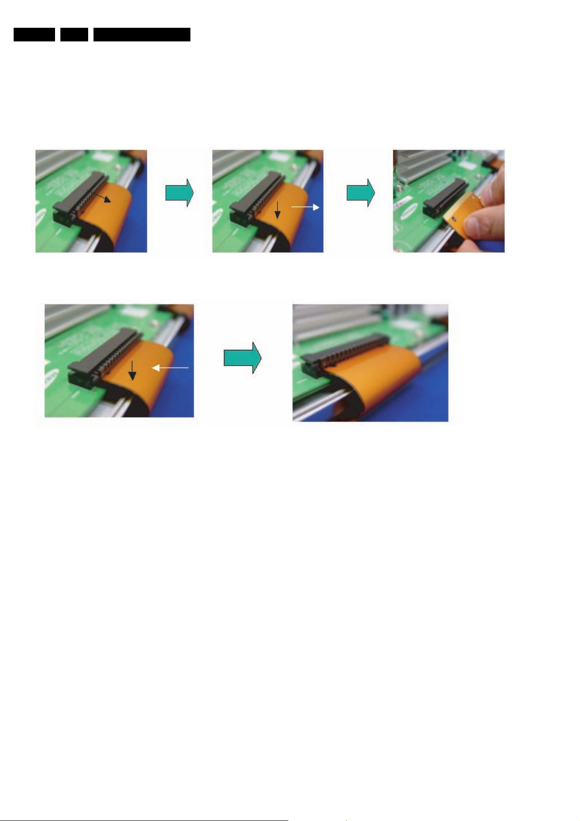
4.1.2 Flat Cable Connector of X-main Board
• Dis-assembly:
1. Pull out the clamp of connector.
2. Pull Flat cable out press down lightly.
3. Turn the Flat Cable reversely.
• Re-assembly: Put the Flat Cable into the connector press
down lightly until locking sound (“Click“) comes out.
Figure 4-3 Dis-assembly FCC of X-main board
Mechanical Instructions
Figure 4-4 Re-assembly FCC of X-main board

4.1.3 FFC and TCP from Connector
• Dis-assembling of TCP:
1. Open the clamp carefully.
2. Pull the TCP out from its connector.
• Re-assembling of TCP:
1. Put the TCP into the connector carefully
2. Close the clamp completely (until “Click” comes out.).
Mechanical Instructions
Notes:
• Checking whether the foreign material is on the connector
• Be careful, do not damage the board by ESD during
Figure 4-5 Dis-assembly of TCP
EN 19SDI PDP 4.
inside before assembling of TCP.
handling of TCP.
Figure 4-6 Re-assembly of TCP
Figure 4-7 Mis-assembly of TCP
The procedure of
assembling and disassembling of
FFC is same as TCP
Figure 4-8 Dis- and re-assembly of FFC
EN 20 SDI PDP4.
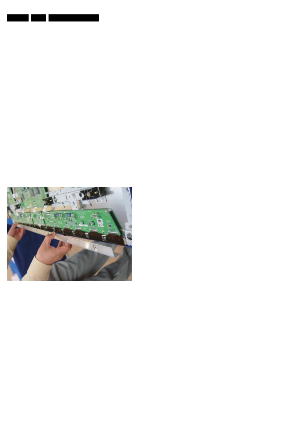
4.1.4 Exchange of LBE, LBF, LBG board
1. Depending on the model (see “Photo 2” per model.):
– 42" SD v3 - Remove the screws in order of 2-3-5-7-1-
4-6 (and 10-11-13-16-9-12-14 for HD) from heat sink
and then remove heat sink (Photo 1).
– 42" SD v4 - Remove the screws in order of 2-4-1-5-3
from heat sink and then remove heat sink (Photo 1).
– 42" HD v3, 37" SD v4, 50" HD v3 - Remove the
screws in order of “Centre - Left Side - Right Side” from
heat sink and then get rid of heat sink (Photo 1).
– 50" HD v4 - Remove the screws in order of 2-3-1-4
from heat sink and then remove heat sink (Photo 1).
2. Remove the TPC, FFC, and power cable from the
connectors.
3. Remove all the screws from the defective board.
4. Remove the defected board.
Note: When replacing the Logic board or Y-main board for
a lead-free (Pb-free) board, always replace them together.
(this is only valid for the 37” SD v4 displays!)
5. Replace the new board and then screw tightly.
6. Clean the connectors.
7. Re-connect the TCP, FFC, and power cable to the
connector.
8. Re-assemble the TCP heat sink. Use the same screw
mounting order as described above
Mechanical Instructions
Caution: If you screw too tight, it is possible to damage the
Driver IC of the TCP.
Figure 4-9 Photo 1 - Heatsink removal
Mechanical Instructions
EN 21SDI PDP 4.
Left
Centre Right
Figure 4-10 Photo 2 - 37” SD v4
4 6 17 532
Figure 4-11 Photo 2 - 42” SD v2 and v3

EN 22 SDI PDP4.
Mechanical Instructions
1
2
3
Figure 4-12 Photo 2 - 42” SD v4
XYG Z[G \G]G ^_
4
5
F_14991_028.eps
030805
YY
1
2
`XW XXXY X[G X\X] XZ
Figure 4-13 Photo 2 - 42” HD v3
3
Figure 4-14 Photo 2 - 42” HD v4
4
5
F_14991_028.eps
030805

Mechanical Instructions
F_14991_029.eps
030805
ཛGཛྷཝཞ
ཛ
G
ཛྷཝཞ
G
EN 23SDI PDP 4.
Left Centre Right
Figure 4-15 Photo 2 - 50” HD v3
Figure 4-16 Photo 2 - 50” HD v4
EN 24 SDI PDP4.
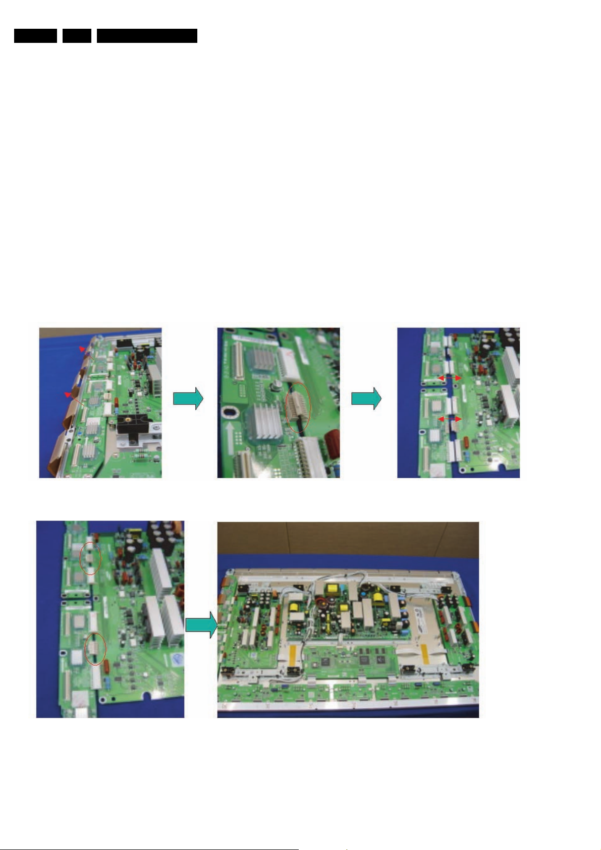
4.1.5 Exchange YBU, YBL and YM board
1. Separate all the FPC connector s of YBU (Y-Buffer upper)
and YBL (Y-Buffer lower). See “Photo 1”.
2. Separate all the connector of CN5001 and CN5008 from YMain. See “Photo 2”.
3. Loosen all the screws of YBU, YBL, and YM. See “Photo
3”.
4. Remove the board from chassis.
5. Remove the connector of CN5006 and CN5007 among
YBU, YBL and YM.
6. Remove the YBL and YBU from Y-main.
7. Remove the defected board.
Note: When replacing the Logic board or Y-main board for
a lead-free (Pb-free) board, always replace them together.
(this is only valid for the 37” SD v4 displays!)
8. Re-assemble the YBU and YBL to the Y-Main.
9. Connect the connector of CN5006 and CN5007 among
YBU, YBL and YM. See “Photo 4”.
10. Arrange the board on the chassis and then screw to fix.
11. Connect the FPC and YM of panel to the connector. See
“Photo 5”.
12. Supply the electric power to the module and then check the
waveform of the board.
13. Turn “off” the power after the waveform is adjusted.
Mechanical Instructions
Figure 4-17 Photo 1, 2, and 3: Dis-assembly of YBU, YBL, and YM
Figure 4-18 Photo 4 and 5: Re-assembly of YBU, YBL, and YM
 Loading...