

Page 1

DVD-Video Player DVD Module SD-5.31SL
Contents Page
1 Technical Specifications 2
2 Safety Instructions, Warnings, and Notes 5
3 Directions for Use (not available) 6
4 Mechanical Instructions 7
5 Test Instructions Mono Board SD5.31SL 11
Diagnostic Software Description 20
6 Block Diagram and Testpoint Overview
Block Diagram 31
TTestpoint Overview Bare Board 32
7 Electrical Diagrams & Pwb’s Diagr. PWB
DVD Analog Front-end (Diagram M1) 33 41-46
Spindle/Servo Motor Driver (Diagram M2) 34 41-46
DVD Front-end Processor (Diagram M3) 35 41-46
DVD Back-end Processor (Diagram M4) 36 41-46
Back-end Memory (Diagram M5) 37 41-46
Audio (Diagram M6) 38 41-46
Services and Debug (Diagram M7) 39 41-46
Video and Power (Diagram M8) 40 41-46
8 Alignments (not available) 47
9 Circuit Description 47
List of Abbreviations 55
IC Data Sheets 56
10 Spare Part List 61
11 Revision List 64
©
Copyright 2003 Philips Consumer Electronics B.V. Eindhoven, The Netherlands.
All rights reserved. No part of this publication may be reproduced, stored in a
retrieval system or transmitted, in any form or by any means, electronic,
mechanical, photocopying, or otherwise without the prior permission of Philips.
Published by PF0365 Service Singapore Printed in the Netherlands Subject to modification EN 3122 785 13710
Page 2
EN 2 SD-5.31SL1.
Technical Specifications
1. Technical Specifications
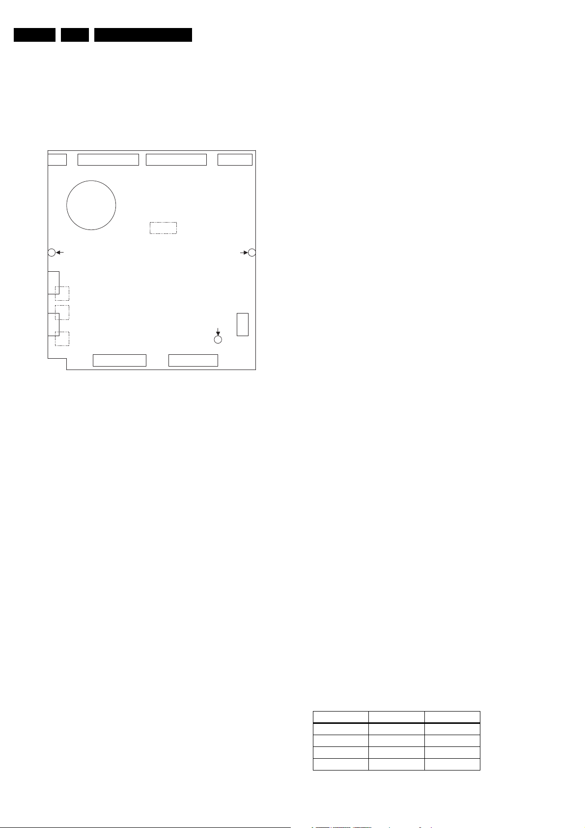
1.1 Interfaces and Pin Assignments
The interfaces or connectors are placed on both PCB layers of
top and bottom as shown in figure "Interfaces placement on
PCB layer".
Basic AV Advance AVExt I2S Digital Video
30 30 124
1
1702
7
1
1402
7
DIAGS
JTAG
15
Screw mounting
1600 18001701
point
Loader conn
124124
Figure 1-1 Interfaces placement on PCB layer
1
OPU
Monoboard
Top view
1300 1301
E-Link/Atapi-2E-Link/Atapi-1
Screw mounting
1
1400
Screw mounting
point
point
CL 36532043_016.eps
Motor
Spindle
210503
151
1100
1.2.2 Interface Basic AV at Location 1600
1. GND
2. DVD_SC
3. GND_SC
4. DVD_L
5. GND_L
6. DVD_R/ PCMDATA3(CELf)
7. GND_R
8. DVD_LFE
9. GND_LFE
10. DVD_LS / PCMDATA2(LsRs)
11. GND_LS
12. DVD_C
13. GND_C
14. DVD_RS/ PCMDATA1(LR)
15. GND_RS
16. SENSE_3V3
17. GND
18. MIC_IN (KOK)
19. GND
20. VIDEO_SEL
21. GND
22. I2CSCL_M
23. I2CSDA_M
24. GND
25. PCMDATA0(LtRt)
26. GND
27. DIG_IN_1
28. I2C INT
29. DAC_RST
30. GND
1.2 Connections
1.2.1 Interface ADVANCE AV at Location 1800:
1. I2CSCL_M / I2CSCL_S
2. I2CSDA_M / I2CSDA_S
3. SCART1 / I2C INT/ GND
4. SCART0 / SLOT_IN_DET
5. B_REF (Video ground)
6. B_U
7. G_REF (Video ground)
8. G_Y
9. R_REF (Video ground)
10. R_V
11. Y_REF (Video ground)
12. Y
13. C_REF (Video ground)
14. C
15. CVBS-REF (Video ground)
16. CVBS
17. +3V3
18. +3V3
19. +5V
20. +12V_Stby
21. +12V
22. MUTE / SPDIF
23. GND
24. PCMSCLK
25. PCMDATA0 / Lt
26. GND_LRT (Audio ground)
27. PCMCLK / Rt
28. PCMLRCLK
29. GND
30. SPDIF / MUTE
1.2.3 Service connector at Location 1702:
1 TXD_SER TXD service UART
2 SERVICE Service or normal mode select
3 RXD_SER RXD service UART
4 RTS_SER Not used
5 GNDB Ground
6 CTS_SER Not used
7 +5V 5V supply
1.3 Signal Specifications
This section defines the specifications of the signals at the
module interface.
1.3.1 Voltage level
TTLTransistor-transistor logic (5V logic)
Caution: Exceeding the absolute maximum rating will cause
damage to the module.
Absolute maximum rating:
IN =-0.5V to 5.5V
VOUT = -0.5V to 5.5V
Table 1-1
Parameter Min Max
VIH (V) 2.0 VIL (V) - 0.8
VOH (V) 2.4 VOL (V) - 0.4
LVTTLLow voltage transistor-transistor logic (3.3V logic)
Page 3
Technical Specifications
EN 3SD-5.31SL 1.
Caution: Exceeding the absolute maximum rating will cause
damage to the module.
Absolute maximum rating:
VIN = -0.5V to 3.8V
VOUT =-0.5V to 3.8V
Maximum current drive: 4mA
Table 1-2
Parameter Min Max
VIH (V) 2.0 VIL (V) - 0.8
VOH (V) 2.4 VOL (V) - 0.4
I2C
• Inter-IC
• All I2C signals at the module's connectors are 5V levels.
I2S
• Inter-IC sound
• All I2S signals at the module's connectors are at LVTTL
levels.
RS232_COMP
• RS232 compatible specifications
• VIN approximately 3V threshold, 6kohm input resistance
• VOUT = 0 to 5V, 1kohm output resistance
H/L
• 5V logic states
• H = +5V ± 0.5V
•L = 0V ± 0.5V
h/l
• 3.3V logic states
•h = +3.3V ± 0.3V
•l = 0V ± 0.3V
1.3.2 SPDIF out
Function : Digital audio output
Signal : SPDIFOUT
Type : Output according to
IEC60958 or
IEC61937, 1Vp-p,
unbalanced.
1.3.3 Audio PCM (I2S format)
Function : Digital audio
Signal : DA_XCK, DA_BCK,
DA_LRCK,
DA_DATA0,
DA_DATA1,
DA_DATA2,
DA_DATA3
Type : I2S output (33ohm
output resistors, in
series)
1.3.4 Analog Audio
Function : Analog audio, 2-ch
Signal : LT, RT
Type : Analog output with on-
bd. 10k load
1.3.5 Audio mute
Function : Audio mute control for
final analog stage
Signal : MUTE
Type : LVTTL output
Table 1-3
Function MUTE
Mute off LOW
Mute on HIGH
1.3.6 Analog video
Function : Analog video
Signal : CVBS_VID, C_VID,
Y_VID, R_VID (V),
G_VID (Y), B_VID (U)
Type : Output (75ohm output
resistors, in series)
1.3.7 Slow blanking SCART
Function : Slow blanking SCART
(0/6/12)
Signal : SCART0, SCART1
Type : LVTTL output
Table 1-4
Function SCART0 SCART1
TV display HIGH HIGH
TV display LOW HIGH
16:9 aspect ratio HIGH LOW
4:3 aspect ratio LOW LOW
Note: SCART0 & SCART1 are legacy features. They were
used to generate 0/6/12 signal on an ext. A/V bd. However,
most TV/Audio sets have their own Scart control ic & hence
these 2 pins have alternate functions via optional jumpers.
SCART1 shares with I2C_INT & GND; SCART0 pin shares
with SLOT_IN_DETECT.
1.3.8 Slave I2C
Function : Slave I2C bus
(Hardware)
Signal : S_I2C_CL;
S_I2C_DA
Type : I2C
Note: I2C lines are pulled to +5V.
1.3.9 Master I2C
Function : Master I2C bus
(Software)
Signal : M_I2C_CL;
M_I2C_DA
Type : I2C
Note: I2C lines are pulled to +5V.
Page 4
EN 4 SD-5.31SL1.
Technical Specifications
1.3.10 27MHz clock
Function : Output a 27MHz clock
signal
Signal : VCLK
Type : LVTTL output
(100ohm output
resistor, in series)
Note: This VCLK pin has dual functionality. It provides 27 Mhz
when Digital video output is used & as
This VCLK pin has dual functionality. It provides 27 Mhz when
Digital video output is used & as an input for PCM_CLK when
ext. I2S is used. Option jumpers are provided.
Exercise caution when connecting to this line; excessive
loading can cause noise and increase jitter levels & degrade
the quality of SPDIF and I2S signals.
1.3.11 Service bus
Function : Service and
diagnostic bus
Signal : TXD_SER,
RXD_SER
Type : RS232_COMP
(TXD_SER output,
RXD_SER input)
1.3.12 Service activation
Function : To activate service/
diagnostic mode
Signal : SERVICE
Type : LVTTL input
Table 1-5
: Watermark detect and
decode for DVDaudio
1.4.1 Analog video performance
The video output standard follows the source material. The
OSD can be switched between PAL and NTSC.
The module has 6 analog video outputs in 4 format: CVBS, Y/
C, and RGB (YUV). However, depending on the module
configuration, not all output can be available at the same time.
Table 1-6
Signal name Video format
CVBS_VID CVBS
Y_VID, C_VID Y/C
R_VID (V) / G_VID (Y) / B_VID (U) RGB (YUV)
1.4.2 Option Jumpers:
J1, J2 & J3 hard select the required video output on Connector
1800. Alternatively, pre-determined Software setting, via slash
option, is also possible. DAC's that are not in used should be
turned off.
Note: RGB and YUV component video signals shared the
same lines. Therefore, the module is not able to output both
RGB and YUV at the same time.
Superimposed DC level : 1.2V
Output impedance : 75ohm
Signal-to-noise ratio : better than 65dB
Video bandwidth : 8MHz (± 3dB) /
16MHz (± 3dB) for
progressive scan
Function SERVICE
Service mode LOW (or pulled to ground)
Normal mode HIGH (or unconnected)
Note: This line is pulled to HIGH via 10kohm resistor. A module
reset is required to activate service mode.
1.4 Audio Format (I2S)
Function : Digital audio
Signal : DA_XCK, DA_BCK,
DA_LRCK,
DA_DATA0,
DA_DATA1, DA_A
Additional 2 channels : downmixed stereo/
LtRt - optional
Sampling rate : MPEG-1, MPEG-2,
Dolby Digital, DTS
and DVD-Audio up to
192 kHz
Decoding : MPEG-1 and -2,
Layers I, II, and III
(MP3); MPEG-2 5.1;
: Dolby Digital Class A;
MLP; DTS; Dolby Pro
Logic; HDCD
Copy protection : CPPM for
prerecorded media
(DVD-audio)
: CPRM for recordable
media (DVD-audio)
Copy protection : CSS
: Macrovision Version
7.1.L.1 for NTSC/PAL
interlaced video
outputs
: Macrovision AGC
1.03 for 480P
progressive scan
video output
Page 5
Safety Instructions, Warnings, and Notes
2. Safety Instructions, Warnings, and Notes
EN 5SD-5.31SL 2.
2.1 Safety Instructions
2.1.1 General Safety
Safety regulations require that during a repair:
• Connect the unit to the mains via an isolation transformer.
• Replace safety components, indicated by the symbol ,
only by components identical to the original ones. Any
other component substitution (other than original type) may
increase risk of fire or electrical shock hazard.
Safety regulations require that after a repair, you must return
the unit in its original condition. Pay, in particular, attention to
the following points:
• Route the wires/cables correctly, and fix them with the
mounted cable clamps.
• Check the insulation of the mains lead for external
damage.
• Check the electrical DC resistance between the mains plug
and the secondary side:
1. Unplug the mains cord, and connect a wire between
the two pins of the mains plug.
2. Set the mains switch to the 'on' position (keep the
mains cord unplugged!).
3. Measure the resistance value between the mains plug
and the front panel, controls, and chassis bottom.
4. Repair or correct unit when the resistance
measurement is less than 1 MΩ.
5. Verify this, before you return the unit to the customer/
user (ref. UL-standard no. 1492).
6. Switch the unit ‘off’, and remove the wire between the
two pins of the mains plug.
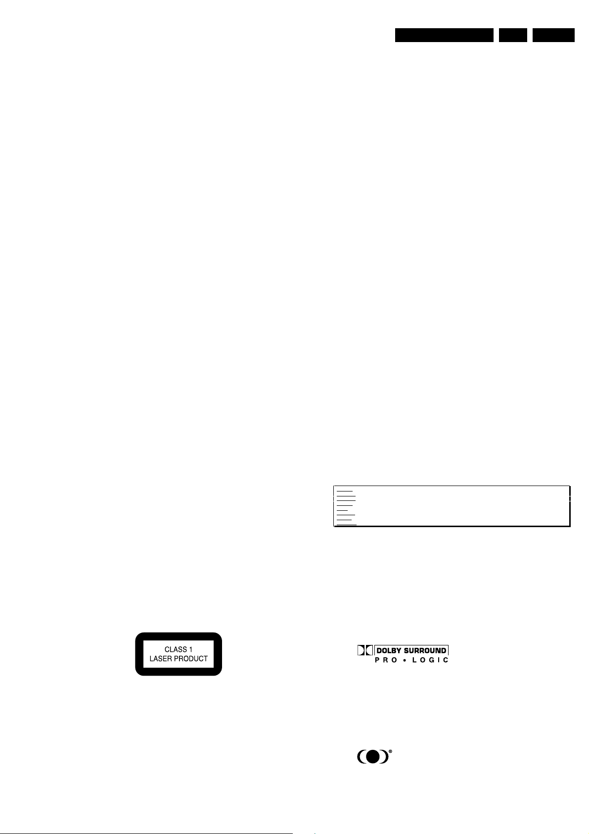
2.1.2 Laser Safety
This unit employs a laser. Only qualified service personnel may
remove the cover, or attempt to service this device (due to
possible eye injury).
2.2 Warnings
2.2.1 General
• All ICs and many other semiconductors are susceptible to
electrostatic discharges (ESD, ). Careless handling
during repair can reduce life drastically. Make sure that,
during repair, you are at the same potential as the mass of
the set by a wristband with resistance. Keep components
and tools at this same potential. Available ESD protection
equipment:
– Complete kit ESD3 (small tablemat, wristband,
connection box, extension cable and earth cable) 4822
310 10671.
– Wristband tester 4822 344 13999.
• Be careful during measurements in the live voltage section.
The primary side of the power supply (pos. 1005), including
the heatsink, carries live mains voltage when you connect
the player to the mains (even when the player is 'off'!). It is
possible to touch copper tracks and/or components in this
unshielded primary area, when you service the player.
Service personnel must take precautions to prevent
touching this area or components in this area. A 'lightning
stroke' and a stripe-marked printing on the printed wiring
board, indicate the primary side of the power supply.
• Never replace modules, or components, while the unit is
‘on’.
2.2.2 Laser
• The use of optical instruments with this product, will
increase eye hazard.
• Only qualified service personnel may remove the cover or
attempt to service this device, due to possible eye injury.
• Repair handling should take place as much as possible
with a disc loaded inside the player.
• Text below is placed inside the unit, on the laser cover
shield:
Laser Device Unit
Type : Semiconductor laser
GaAlAs
Wavelength : 650 nm (DVD)
: 780 nm (VCD/CD)
Output Power : 20 mW (DVD+RW
writing)
: 0.8 mW (DVD
reading)
: 0.3 mW (VCD/CD
reading)
Beam divergence : 60 degree
Figure 2-1
Note: Use of controls or adjustments or performance of
procedure other than those specified herein, may result in
hazardous radiation exposure. Avoid direct exposure to beam.
CAUTION VISIBLE AND INVISIBLE LASER RADIATION WHEN OPEN AVOID EXPOSURE TO BEAM
ADVARSEL SYNLIG OG USYNLIG LASERSTRÅLING VED ÅBNING UNDGÅ UDSÆTTELSE FOR STRÅLING
ADVARSEL SYNLIG OG USYNLIG LASERSTRÅLING NÅR DEKSEL ÅPNES UNNGÅ EKSPONERING FOR STRÅLEN
VARNING SYNLIG OCH OSYNLIG LASERSTRÅLNING NÄR DENNA DEL ÄR ÖPPNAD BETRAKTA EJ STRÅLEN
VARO! AVATTAESSA OLET ALTTIINA NÄKYVÄLLE JA NÄKYMÄTTÖMÄLLE LASER SÄTEILYLLE. ÄLÄ KATSO SÄTEESEEN
VORSICHT SICHTBARE UND UNSICHTBARE LASERSTRAHLUNG WENN ABDECKUNG GEÖFFNET NICHT DEM STRAHL AUSSETSEN
DANGER VISIBLE AND INVISIBLE LASER RADIATION WHEN OPEN AVOID DIRECT EXPOSURE TO BEAM
ATTENTION RAYONNE MENT LASER VISIBLE ET INVISIBLE EN CAS D'OUVERTURE EXPOSITION DANGEREUSE AU FAISCEAU
!
Figure 2-2
2.2.3 Notes
Dolby
Manufactered under licence from Dolby Laboratories. “Dolby”,
“Pro Logic” and the double-D symbol are trademarks of Dolby
Laboratories. Confidential Unpublished Works. ©1992-1997
Dolby Laboratories, Inc. All rights reserved.
Figure 2-3
Trusurround
TRUSURROUND, SRS and symbol (fig 2-4) are trademarks of
SRS Labs, Inc. TRUSURROUND technology is manufactured
under licence frm SRS labs, Inc.
Figure 2-4
Page 6

EN 6 SD-5.31SL3.
3. Directions for Use
There is no DFU available
Directions for Use
Page 7
4. Mechanical Instructions
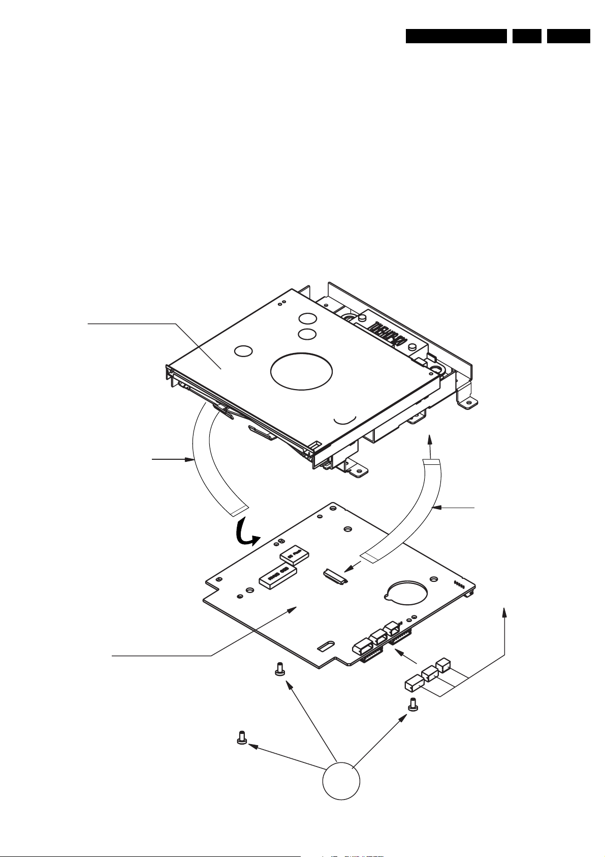
4.1 Dismantling Instruction
Dismantling Instruction
1. Unplug 3 conn [C] from Monoboard [D].
2. Unlock conn 1100 on Monoboard [D] and gentlely unplug Flex [B].
3. Remove 3 screws [F].
4. Separate Monoboard [D] gentlely from loader [E] and beware of the Flex [A].
5. Unlock conn 1001 on the Monoboard [D] and gentlely unplug Flex [A].
Slot-in Loader [E]
Mechanical Instructions
EN 7SD-5.31SL 4.
Flex [B]
Monoboard [D]
To Loader OPU
Flex [A]
from Loader
Conn [C]
Figure 4-1
F
CL 36532043_021.eps
220503
Page 8
EN 8 SD-5.31SL4.
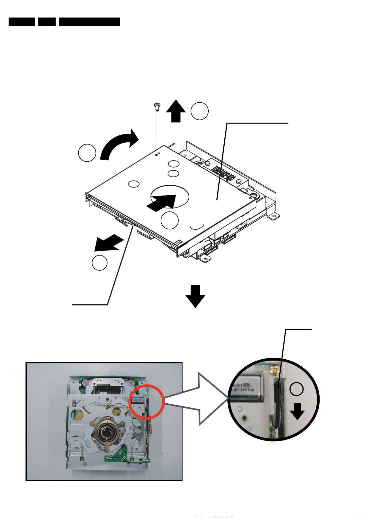
4.1.1 Manually Eject the Disc
See Figure 4-2 eject the disc manually.
1. Remove screw,
2. Slide top cover backward,
3. Flip top cover and remove it,
4. Turn the belt in the anti-clockwise direction with your thumb
till the disc is ejected,
5. Gently pull the disc out.
Mechanical Instructions
3
5
2
1
Top Cover
Slot
Belt
4
CL 36532043_022.eps
020603
Figure 4-2 Manually eject the disk
Page 9
Mechanical Instructions
solder joint
EN 9SD-5.31SL 4.
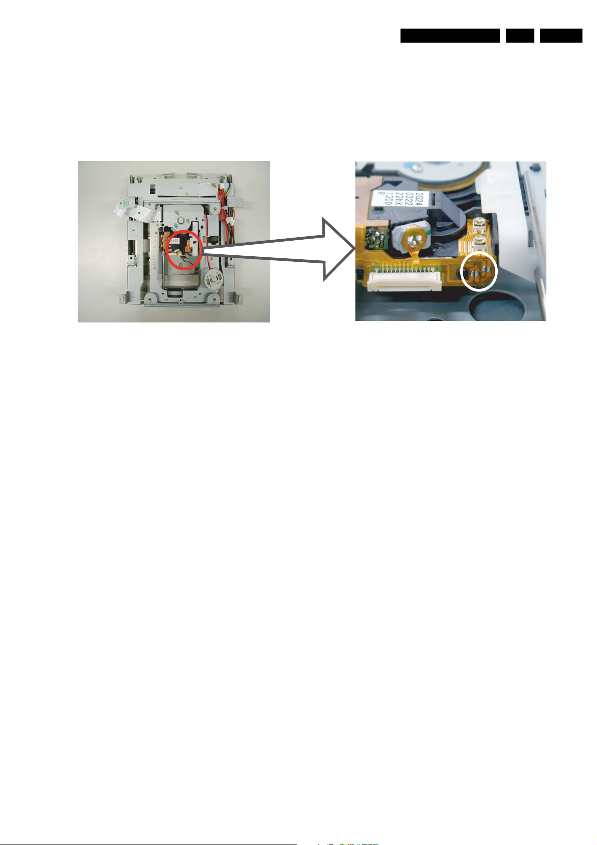
4.2 Service Hints
4.2.1 Repair tips
DVD Module SD5.31SL
The DVD module is an integrated unit of TOHEI SLOT-IN
loader and Monoboard.
TOHEI SLOT-IN Loader
The loader is a non-repairable unit and in case of failure, it has
to be replaced with a new loader.
When replacing with a new Slot-in loader, two solder joints
have to be removed after connecting the OPU flex foil to the
Monoboard. The solder joints which short circuits the laser
diodes to ground are for protection against ESD. Refer to
Figure "ESD solder joint" for location of solder points.
CL 36532043_018.eps
020603
Monoboard
The Monoboard has to be repaired down to components level.
Repair handling of the Monoboard requires a workshop with
sophisticated de-soldering tools.
4.2.2 Change of Slash number setting
The software setting can be change according to the following
procedure:
1. Press PLAY< 159>
2. Enter the 8-digit code <2><2><2><0><0><5><0><0> on
the remote control.
3. Press PLAY.
4. The change should effect immediately with information
indicated on TV screen.
4.2.3 Software upgrade via Download disc
Both the application and servo software can be flashed into the
DVD player by means
of a CD-ROM disc. The CD-ROM disc has to be made with a
CD writer SW.
Application software
1. Insert the Upgrade disc into the player.
2. The upgrading operation will start automatically.
3. Once the upgrading process finishes, the player will
automatically eject the disc.
4. Remove the Upgrade disc.
5. The player will be restarted automatically and display on
TV screen will show
Figure 4-3 ESD solder joint
recommended to write only this file into the disc &
write it in DAO ie. Disc At Once mode.
2. Upgrading procedure
3. Power-on the module.
4. Insert the Upgrading disc. Make sure that this is the first
disc that the module sees, otherwise the module will treat
it as a general cd-rom disc & not perform the upgrade.
5. The upgrading process takes about 10 secs. & when it
finishes, the disc will be ejected.
6. Power sequence the module for the new code to take
effect.
Servo software
1. First, make the CD-R/CD-RW:-
• Disc format
– The disc format must be CD-ROM Mode 1 and
ISO9660 format.
• Writing mode
– The volume name (Label) of the disc must be
"ALI_CODE" & the file name of the upgrading
firmware must be "PS57.BIN". You must put the
file as the first item in the disc.Highly
Page 10

EN 10 SD-5.31SL4.
4.2.4 Verify setting
To check that the setting has change successfully.
1. Press button on the remote control while disc tray is open.
2. The texts will appear on the TV screen. That is how it looks
like.
– Copyright©
– Philips 2002-03
– SD5.31-34
– 30May2003
– 15:42
– 22200500
– A1133
– C3091
– 100305R3424
In the texts, the following numbers refer to:
• SD5.31-34 ==> refer to Application software version
• 30May2003 ==> refer to date software was upgraded
• 15:42 ==> refer to time software was upgraded
• 22200500 ==> refer to Slash version
• 100305R3424 ==> refer to servo software version
4.2.5 Test disc
The following test discs are recommended for use to test the
playability of the player.
• DVD disc: MPTD CVP 02.18- 12nc 7104 099 91691
• Audio disc (CDDA): Subchassis 8a Test disc- 12nc 7104
099 28362
Mechanical Instructions
4.2.6 Ejecting Disc
When ejecting disc is not possible using remote control
• Short circuit test land [F220] to ground when power
supplies are still present with assumption the front end is
not faulty.
• When above is not possible, ejecting of the disc has to be
done manually. Refer to instruction "Manually Ejecting of
disc".
4.2.7 ComPair
For assistance with the repair process of the Monoboard,
electronic fault finding guidance has been developed. This
program is called ComPair. This ComPair program is available
on CDROM. The version of the CDROM for repair of the
monoboard is V1.3 or higher and can be ordered with
codenumber 4822 727 21637. The procedure for registration is
explained in the help file of the program and in the CDROM
booklet. The cable to connect the Monoboard with a PC can be
ordered with codenumber: 3122 785 90017. All the hardware
and software requirements of the systems, necessary for
working with ComPair, are described on the CDROM
Page 11
Test Instructions Mono Board SD5.31SL
PM3380B
5. Test Instructions Mono Board SD5.31SL
5.1 General
EN 11SD-5.31SL 5.
• Impedance of measuring-equipment should be > 1MΩ.
• Most tests have to be done by software commands.
Together with the software command you will find a Ref.#
nbr. This is the number of the diagnostic nulceus used for
this test. More detailed information can be find in the
chapter “Diagnostic Nuclei”.
• Levels: Most measurements are digital measurements.
The signal levels specification in this document are defined
in the chapter Technical Specifications.
• All the waveforms measurement carried out in these test
instruction will be base on the testpoint indicated in the
Monoboard schematic diagram in the service manual.
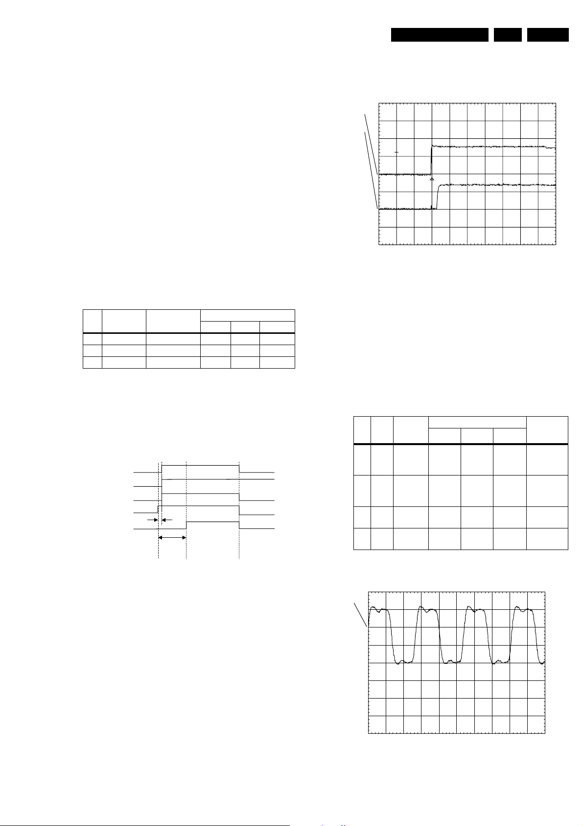
5.2 General Start-up Measurements
5.2.1 Supply Check:
Table 5-1 Supply check
No Testland Signal Name
1 F810 +3V3 3.15V 3.30V 3.50V
2 F811 +5V 4.75V 5.00V 5.25V
3 F813 +12V 10.0V 12.0V 13.2V
The monoboard operates in power-off and power-on mode
only. There is no standby mode. In power-off mode, the
monoboard does not respond to any communication or signals.
Reset is via an internal reset circuit, which are tied to the +3V3
supply. To ensure proper power recycling, the following timing
should be observed:
+12V
+12VSTBY
+3.3V
+5V
Internal
Reset
Modes:-
+12V
0V
+12V
0V
+3.3V
0V
+5V
0V
3ms min
High
Low
Power-off
50ms min
Reset mode Operational mode
DC Voltage (V)
Min Typ Max
CL 36532043_044.eps
Standby mode
270503
ch1
ch2
T
1
2
CH1 1.00V=
CH2 1.00V= MTB 500ms 4.96dv ch1+
Figure 5-2 Reset
NB: The SYS_RST rising edge,CH2, should be at least
100msec after the +3V3ST (refer to CH1 Figure Reset).
If the reset input does not go high then check the reset circuit
around IC7500.
5.2.3 Clock Check
To check the correct functioning of the ZIVA, we first have to
check the presence of all clocks.
Table 5-2 Clock check
Test
No
land
Signal
name
Frequency (MHz)
Min Typ Max
1 F401 XTAL 13.4993 13.5000 13.5007
2 F209 ALI_CLK 33.6994 33.8688 34.0382
3 F421 DA_XCK 18.063 18.432 18.801
4 F502 SD_CLK 119.070 121.500 123.930
CL 36532043_067.eps
030603
Descrip-
tion
Back-end
clock
(± 50ppm)
Front-end
clock
(± 0.5%)
Audio
clock
SDRAM
clock
5.2.2 Reset Check:
Figure 5-1 Timing chart
All tests that require the diagnostic software should be
performed in power-on mode only.
To ensure a proper start-up of the monoboard, the back-end
reset signal SYS_RST is required at the ZIVA-5 input (testpoint
F501) after power-on.
To check the reset timing, measure the SYS_RST (testpoint
F501) and the +3V3ST supply (testpoint F503), reset circuit
trigger signal.
PM3380B
ch1 ch1 freq 18.5Mhz
1
CH1 1.00V= MTB 20.0ns ch1+
Figure 5-3 DA_XCK
CL 36532043_057.eps
030603
Page 12
EN 12 SD-5.31SL5.
Test Instructions Mono Board SD5.31SL
PM3380B
ch1 ch1 freq 13.5MHz
1
CH1 1.00V= MTB 50.0ns ch1+
Figure 5-4 XTAL
PM3380B
ch1 ch1 freq 123MHz
1
CL 36532043_083.eps
030603
Table 5-3 PC connection
Connector pin Signal
1702-1 TXT_SER (service port/UART transmit)
1702-2 SERVICE (service/normal mode select)
1702-3 RXD_SER (service port/UART receive)
1702-4 Not in use
1702-5 GND
1702-6 Not in use
1702-7 +5V_SER
Now start the terminal program. Make sure that the service-pin
(pin 1702-2) of the µP is pulled low.
The terminal program of your PC should now display: “DVDv6
Diagnostic software version ...”. This message already means
that the µP is running. This is also an indication that the first
basic nucleus (nucleus number 1) has been executed during
diagnostic start-up. The other commands can be carried out by
selecting the “command input” and simply type the reference
nbr. to do the test or select the “Menu - driven” test.
To be sure that the µP is able to run the diagnostic software,
serial port will be checked during start-up.
Table 5-4 Serial port check
Ref. # Reference Name Remark
(1) BasicSpAcc Serial port Access test/
initialisation
CH1 1.00V= MTB 5.00ns ch1+
Figure 5-5 SD_CLOCK
PM3380B
ch1: freq= 33.8MHz
ch1
CH1 2.00 V= MTB50.0ns ch1+
Figure 5-6 ALI_CLOCK
5.3 µP Environment:
5.3.1 General:
CL 36532043_072.eps
030603
CL 36532043_070.eps
050603
With this test, the serial communication is checked in both
directions.
5.3.2 Memory Check:
The Flash can be check for failure with the PapChksFl
command.
Table 5-5 Memory check
Ref. # Command Name Remark
6 PapChksFl Checksum FLASH
The PapChksFI calculate and verify checksum of the FLASH.
This includes the entire binary ROM image checksum.
5.4 General I/O Port & Peripherals Check
5.4.1 I2C Bus/NVRAM Check
To access the NVRAM, the I2C bus is used. So by writing and
reading to the NVRAM the chip and the bus is checked. With
next commands a certain byte is written to the NVRAM. The
original information will always be written back into the
NVRAM.
Table 5-6 I2C/NVRAM check command
Ref. # Command Name Remark
11 PapI2cNvram I2C NVRAM access
All the tests are carried out by diagnostic software. To start the
diagnostic software, connect a PC to the serial bus of the ZIVA.
Use connector 1702 for this connection.
The complete NVRAM can also be checked on failures by
writing to all addresses and reading back. This test takes a long
time (110 sec).
Page 13
Test Instructions Mono Board SD5.31SL
PM3380B
EN 13SD-5.31SL 5.
Table 5-7 NVRAM Write/Read check command
Ref. # Command Name Remark
15 PapNvramWrR NVRAM Write Read
5.4.2 Audio Clock Check
The internally generated Audio clock can be set to either 44.1
kHz (CD_DA), 48 kHz (DVD) or 96 kHZ (DVD). To check the
different mode, use the following commands and measure the
waveform as correct operation cannot be detected by the
Diagnostic Software.
Table 5-8 Audio clock check
Command
Ref #
Name Remark
8a PapSgsAclk
Cdda
Internal PLL
CLK in CD-DA
Test
point Frequency
F421 16.934 MHz
mode (Fig 5-4)
8b PapSgsAclk
Dvd
Internal PLL
CLK in DVD
F421 18.432 MHz
mode (Fig 5-5)
8c PapSgsAclk
Dvd96
Internal PLL
CLK in DVD
F421 36.864 MHz
mode (Fig 5-6)
± 0.02%
± 0.02%
± 0.02%
PM3380B
ch1 ch1 freq 36.9MHz
1
CH1 1.00V= MTB 20.0ns ch1+
Figure 5-9 Internal PLL CLK in DVD96kHz mode
5.4.3 Audio Mute Check
Switch on the Mute circuit by sending next command:
Table 5-9 Audio mute ON check command
Ref. # Command Name Remark
19a AudioMuteOn AudioMuteOn
CL 36532043_060.eps
030603
ch1 ch1 freq 18.5Mhz
1
CH1 1.00V= MTB 20.0ns ch1+
Figure 5-7 Internal PLL CLK in CDDA mode
PM3380B
ch1 ch1 freq 18.4MHz
1
CL 36532043_057.eps
030603
Check the Mute output again at testpoint F603: 3V3 ± 10%
Switch off the Mute circuit by sending next command
Table 5-10 Audio mute OFF check command
Ref. # Command Name Remark
19a AudioMuteOff AudioMuteOff
Check the Mute output at testpoint F603: 0V ± 0.3V
5.4.4 Audio I2S Check
To check the audio output from the internal audio DAC on the
Monoboard, execute the following commands and observe the
I2S audio outputs for both sine and pink noise.
Table 5-11 Audio I2S check commands
Command
Ref. #
21a AudioSineOn Audio Sine
Name Remark Audio outputs
Audio Sine signal On
signal Off
Sine, 1kHz on stereo
Press stop button
20a AudioPinkNoi
seOn
Audio
Pinknoise
Pink Noise on 6
channels
On
20b AudioPinkNoi
seOff
Audio
Pinknoise
Off
CH1 1.0 V= MTB 20.0ns ch1+
CL 36532043_059.eps
Figure 5-8 Internal PLL CLK in DVD48kHz mode
030603
The audio signal (sine or pink noise) will also be present on the
digital ouput (SPDif). This can be checked by connecting an
amplifier with digital input.
Check the I2S output.
Page 14
EN 14 SD-5.31SL5.
Test Instructions Mono Board SD5.31SL
Table 5-12 NameTestpointWaveform
Name Testpoint Description
DA_XCK F421 Audio clock
DA_BCK F822 Audio bit clock
DA_DATA0 pin 27/IC7800 Audio data
DA_LRCK F825 Audio word
SPDIF F821 Audio digital out
PM3380B
ch1 ch1 freq 18.5Mhz
1
CH1 1.00V= MTB 20.0ns ch1+
CL 36532043_057.eps
030603
PM3380B
ch1 ch1 freq 48.1kHz
1
CH1 1.00V= MTB 10.0us ch1+
Figure 5-13 DA_LRCK
PM3380B
ch1
T
CL 36532043_056eps
030603
Figure 5-10 DA_XCK
PM3380B
ch1
CH1: freq 2.31Mhz
1
CH1 1.00V = MTB 200ns ch1+
Figure 5-11 DA_BCK
PM3380B
ch1
ch1 freq 255kHz
CL 36532043_054.eps
030603
1
CH1 2.00V= MTB 200ns ch1+
STOP
CL 36532043_079.eps
030603
Figure 5-14 SPDIF
To switch the audio signal OFF, press the STOP button on the
front.
Without A/V board, the switching levels are as follows:
– DA_DATA1,DA_DATA2 and DA_DATA3 switch between
low and high for pink noise. For sine, this is low.
– DA_DATA0, DA_LRCK, DA_XLK and DA_BCK switches
between low and high for both pink noise and sine.
– SPDIF switches between LOW and HIGH
1
STOP
CH1 1.00V= MTB 2.00us ch1+
Figure 5-12 DA_DATA0
CL 36532043_055.eps
030603
Page 15
Test Instructions Mono Board SD5.31SL
EN 15SD-5.31SL 5.
5.5 VIDEO
5.5.1 Video Output Check
Measure the DC voltages at all video-outputs at conn 1800
while the video signal is turned off: 1V ± 10%
Generate a color-bar via next software commands:
Ref. # Command Name Remark
23a VideoColDencOn Colourbar DENC ON
61a VideoColOutRGB Set Video out to RGB
61b VideoColOutYUV Set Video out to YUV
23b VideoColDencOff Colourbar DENC/MPEG OFF
Check video output at the next testpoints:
Name Testpoint Waveform
R_V F817 Refer to Figure R_V
G_Y F816 Refer to Figure G_Y
B_U F815 Refer to Figure B_U
C F819 Refer to Figure C_VIDEO
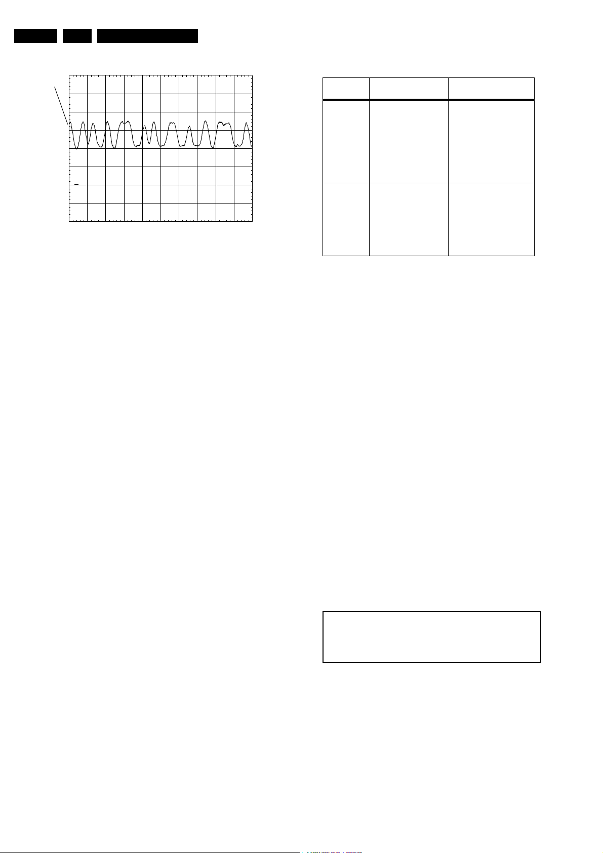
CVBS F820 Refer to Figure CVBS_VID
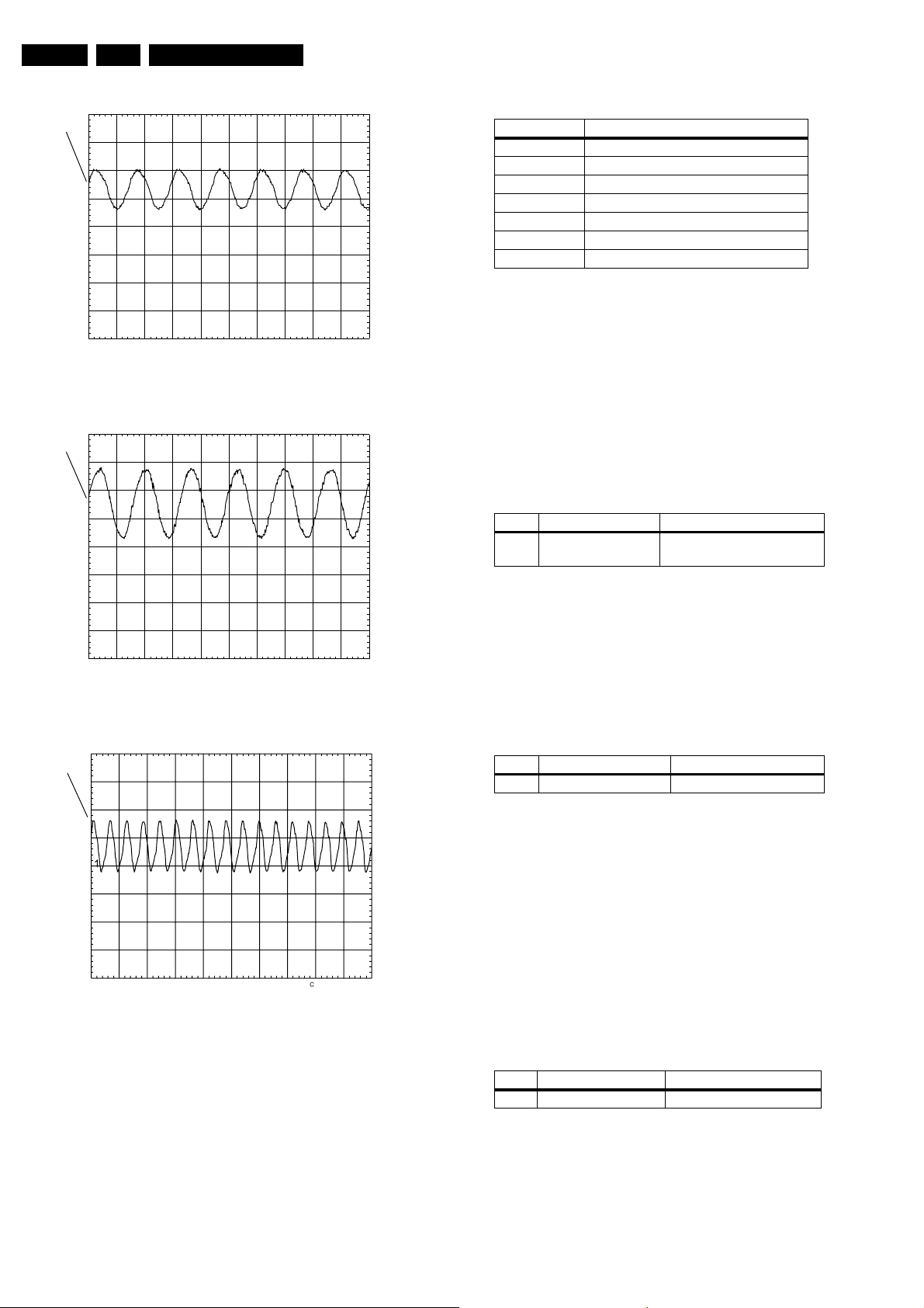
PM3380B
ch1
PM3380B
ch1
1-
CH1 500mV= MTB 20.0us ch1+
Figure 5-17 B_U with video out at RGB
PM3380B
ch1
CL 36532043_050.eps
030603
1
CH1 500nV= MTB 20.0us ch1+
Figure 5-15 R_V with video out at RGB
PM3380B
ch1
1
CH1 500mV= MTB 20.0us ch1+
STOP
Figure 5-16 G_Y with video out at RGB
CL 36532043_069.eps
030603
CL 36532043_062.eps
030603
1
CH1 500mV= MTB 20.0us ch1+
Figure 5-18 CVBS_VID
PM3380B
ch1
1
CH1 500mV= MTB 20.0us ch1+
Figure 5-19 C VIDEO
CL 36532043_053.eps
030603
CL 36532043_052.eps
030603
Page 16
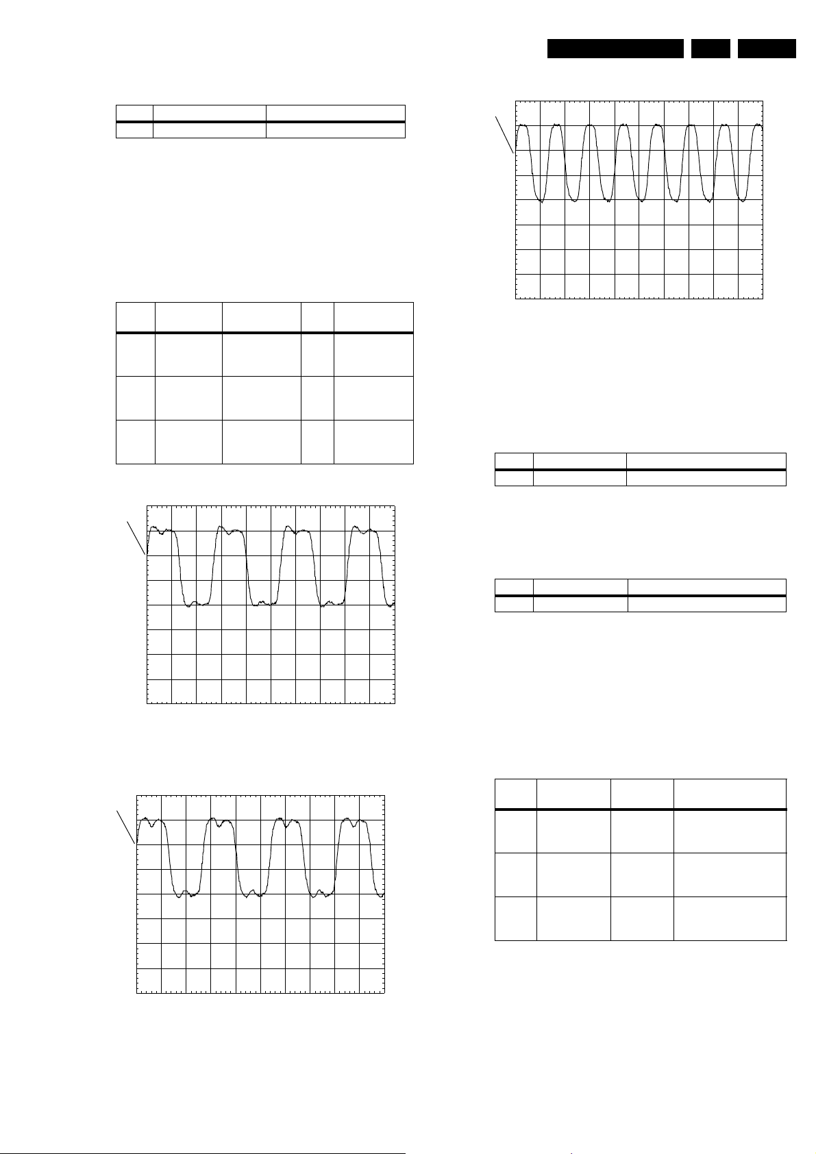
EN 16 SD-5.31SL5.
Test Instructions Mono Board SD5.31SL
PM3380B
ch1
1
CH1 500mV= MTB 20.0us ch1+
Figure 5-20 G_Y with video out at YUV
PM3380B
ch1
CL 36532043_063.eps
030603
5.6 Servo
5.6.1 General Start-up Measurements:
Reset the Basic Engine part
Table 5-13 Reset basic engine command
Ref. # Command Name Remark
44 BeReset Reset the Basic Engine
Check the Servo Reset (IDERST) waveform at pin 50 / IC7200
goes from high to low after executing BeReset commands.
PM3380B
ch1
T
1
1
CH1 500mV= MTB 20.0us ch1+
Figure 5-21 R_V with video out at YUV
PM3380B
ch1
1
CH1 500mV= MTB 20.0us ch1+
CL 36532043_071.eps
030603
CL 36532043_051.eps
030603
CH1 1.00V= MTB 10.0us 4.96dv ch1+
Figure 5-23 IDERST
5.6.2 Spindle Motor check:
The tracking control circuit is checked using the following
commands:
Table 5-14 Spindle check commands
Ref. # Command Name Remark
39a BeDiscmotorOn Discmotor on
39b BeDiscmotorOff Discmotor off
Check the following signals with the discmotor switched ON
with the loader connected and with DVD Disc inserted.
CL 36532043_065.eps
030603
Figure 5-22 B_U with video out at YUV
Page 17
Test Instructions Mono Board SD5.31SL
EN 17SD-5.31SL 5.
Table 5-15 Disc motor switching
Signal
Name Testpoint Frequency
SMOTOR Pin22/IC7101 Output voltage control
SSPDON Pin23/IC7101 Power save
Motor ON - high
Motor OFF - low
VH Pin15/IC7101 HALL Bias
Motor ON - LOW
Motor OFF - HIGH
SFGIN Pin 24/IC7101 Tacho signal output
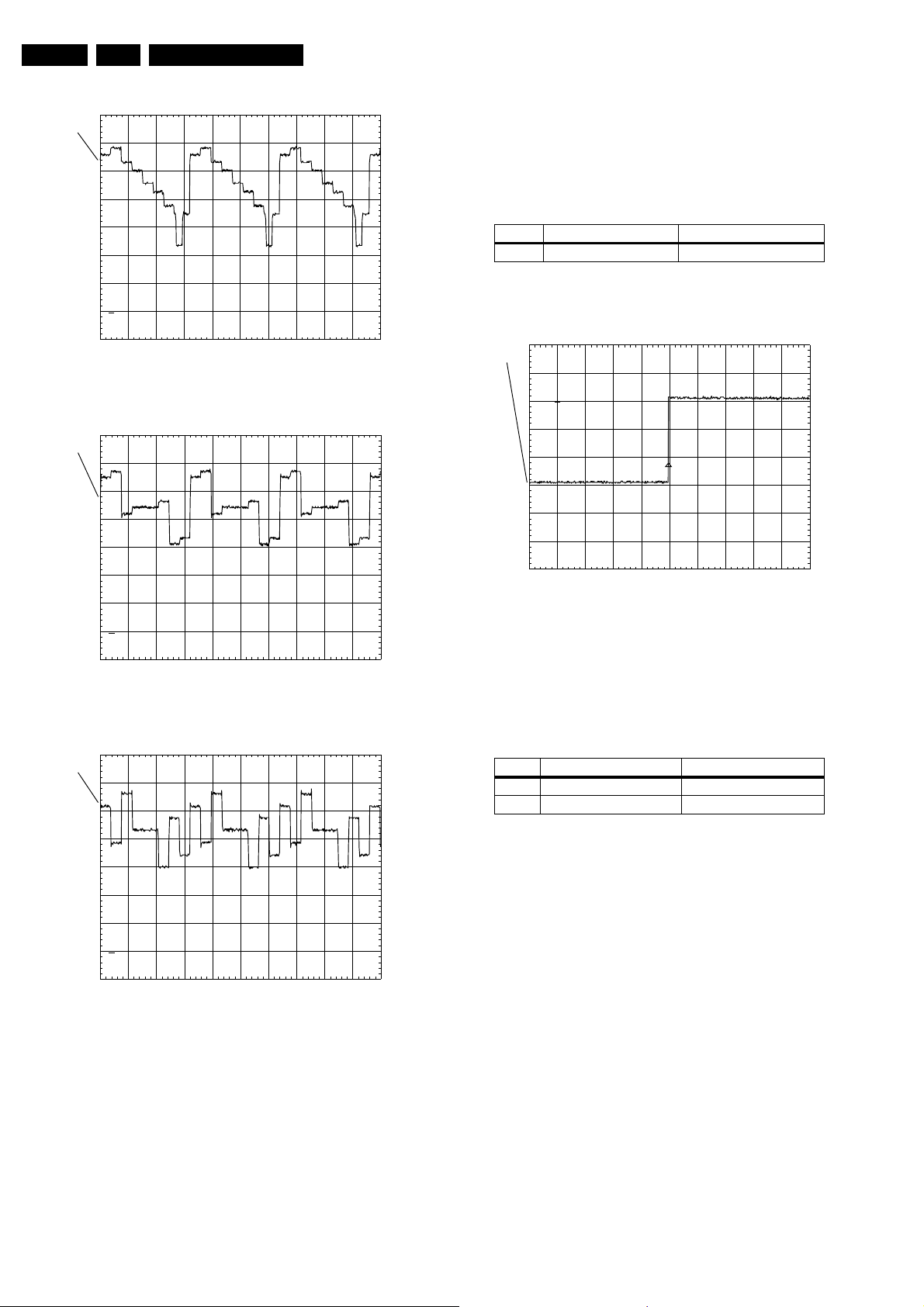
DA1 F113 Output
DA2 F114 Output
DA3 F115 Output
H1+ F112 H1+ HALL input (positive signal)
H1- F111 H1- HALL input (negative signal)
H2+ F110 H2+ HALL input (negative signal)
H2- F109 H2- HALL input (negative signal)
H3+ F108 H3+ HALL input (negative signal)
H3- F107 H3- HALL input (negative signal)
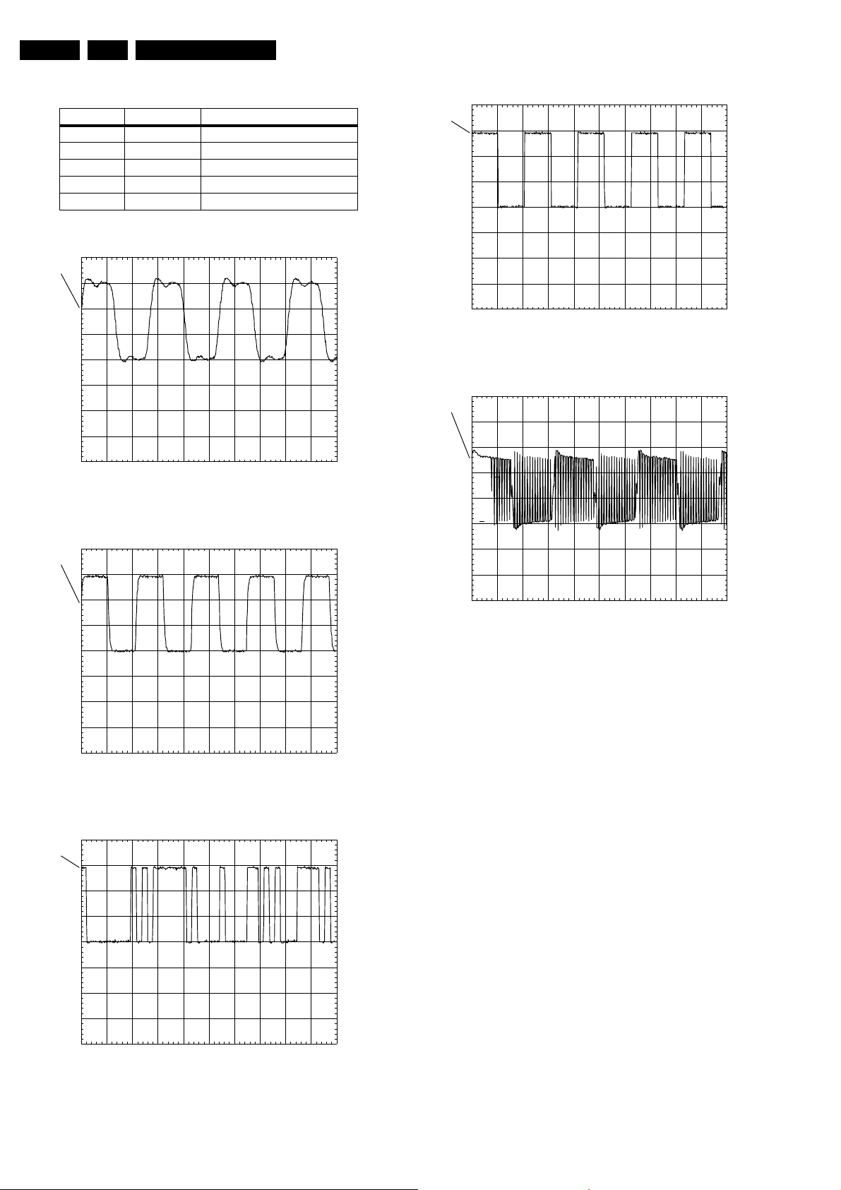
PM3380B
ch1
PM3380B
ch1
T
1
CH1 2.00V= MTB 5.00mus ch1+
STOP
Figure 5-26 DA1-DA2-DA3
PM3380B
ch1
CL 36532043_058.eps
030603
6
CH1 1.00 V= MTB2.00 s- 3.94dv ch1+
CL 36532043_048.eps
Figure 5-24 SMotor (Random during jump track)
PM3380B
ch1
1
CH1 2.00 V= MTB1.00ms ch1+
CL 36532043_049.eps
Figure 5-25 SFGIN
030603
050603
1
CH1 500mV= MTB 5.00ms ch1+
Figure 5-27 HALL input signal
When measurement is completed, switch the discmotor OFF
before executing next command
5.6.3 Tracking check
The tracking control circuit is checked using the following
commands:
Table 5-16 Tracking
Ref. # Command Name Remark
40a BeRadialOn Radial control on
40b BeRadialOff Radial control off
Visual check on the radial ,when Radial control ON, if the
radial movement is visible.
Once the check is completed,switch the Radial control OFF
before executing next command
To check the waveform of TRACK- and TRACK+,
connect a 10W / 0.25W resistor between TRACK- and
TRACK+ to serve as dummy load without connecting the
loader.
CL 36532043_064.eps
030603
Page 18
EN 18 SD-5.31SL5.
Test Instructions Mono Board SD5.31SL
Table 5-17 Trackingl
Signal
Name Testpoint Description
Track - F003 Negative drive to tracking coil
Track + F004 Positive drive to tracking coil
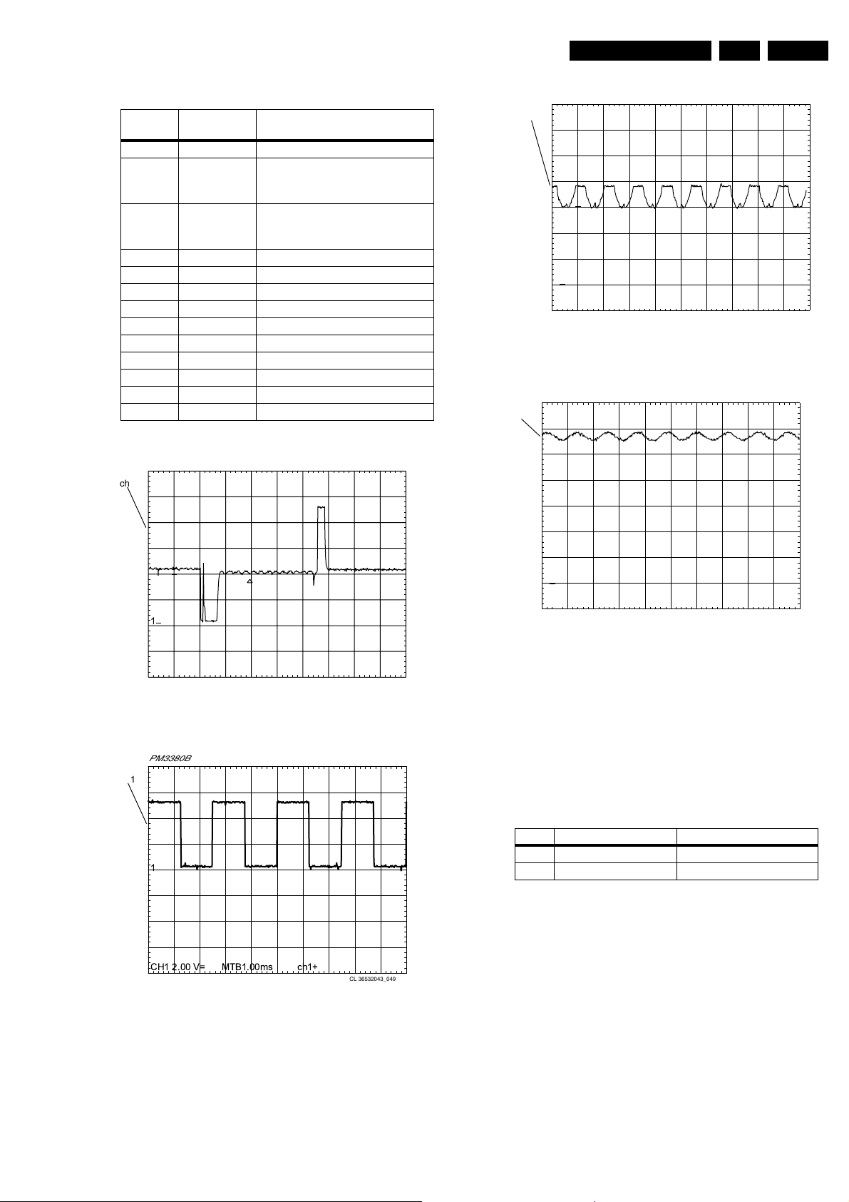
PM3380B
ch1
ch2
T
1
2
CH1 2.00V=
CH1 2.00V= MTB 1.00s 4.18dv ch1+
Figure 5-28 TRACK ON Command
5.6.4 Sledge check
The Sledge control circuit is checked using the following
commands to move the sledge:
Table 5-18 Sledge check commands
CL 36532043_080.eps
030603
PM3380B
ch1
ch2
T
1
CH1 2.00V=
CH2 2.00V= MTB 500ms 5.82dv ch1+
Figure 5-30 SLED Outwards command
5.6.5 Tray Check:
The tray control circuit is checked using the following
command:
Table 5-19 Tray command
Ref. # Command Name Remark
43a BeTrayIn Tray in
43b BeTrayOut Tray out
Measure the DC voltages and waveforms when executing
the tray closed command.
CL 36532043_078.eps
030603
Ref. # Command Name Remark
41a BeSledgeIn Sledge inwards
41b BeSledgeOut Sledge outwards
Visual check on the sledge,when Sledge control ON, if the
sledge movement is visible.
Once the check is completed,switch the Sledge control OFF
before executing next command
To check the waveform of SLEDGE- and SLEDGE+,
connect a 10W / 0.25W resistor between SLEDGE- and
SLEDGE+ to serve as dummy load without connecting the
loader.
PM3380B
ch1
ch2
T
1
CH1 2.00V=
CH2 2.00V= MTB 500ms 5.82dv ch1+
CL 36532043_077.eps
030603
Figure 5-29 SLED Inwards comand
Table 5-20 Tray in
Signal Name Testpoint Value (Tray closed)
LOAD + F116 2V5 +/- 0V2
LOAD - F117 2V5 +/- 0V2
INSW F119 0V +/- 0V2
OUTSW F121 3V +/- 0V2
PM3380B
ch1
T
ch2
1
2
CH1 2.00V=
CH1 2.00V= MTB 500ms 2.24dv ch1+
CL 36532043_081.eps
030603
Figure 5-31 Tray in command
Measure the DC voltages and waveforms when executing the
tray opening command.
Page 19
Test Instructions Mono Board SD5.31SL
EN 19SD-5.31SL 5.
Table 5-21 Tray out
Signal Name Testpoint Value (Tray closed)
LOAD + F116 2V8 ± 0V2
LOAD - F117 2V2 ± 0V2
INSW F119 3V ± 0V2
OUTSW F121 0V ± 0V2
PM3380B
ch1
T
ch2
1
2
CH1 2.00V=
CH1 2.00V= MTB 500ms 2.24dv ch1+
CL 36532043_082.eps
Figure 5-32 Tray out command
030603
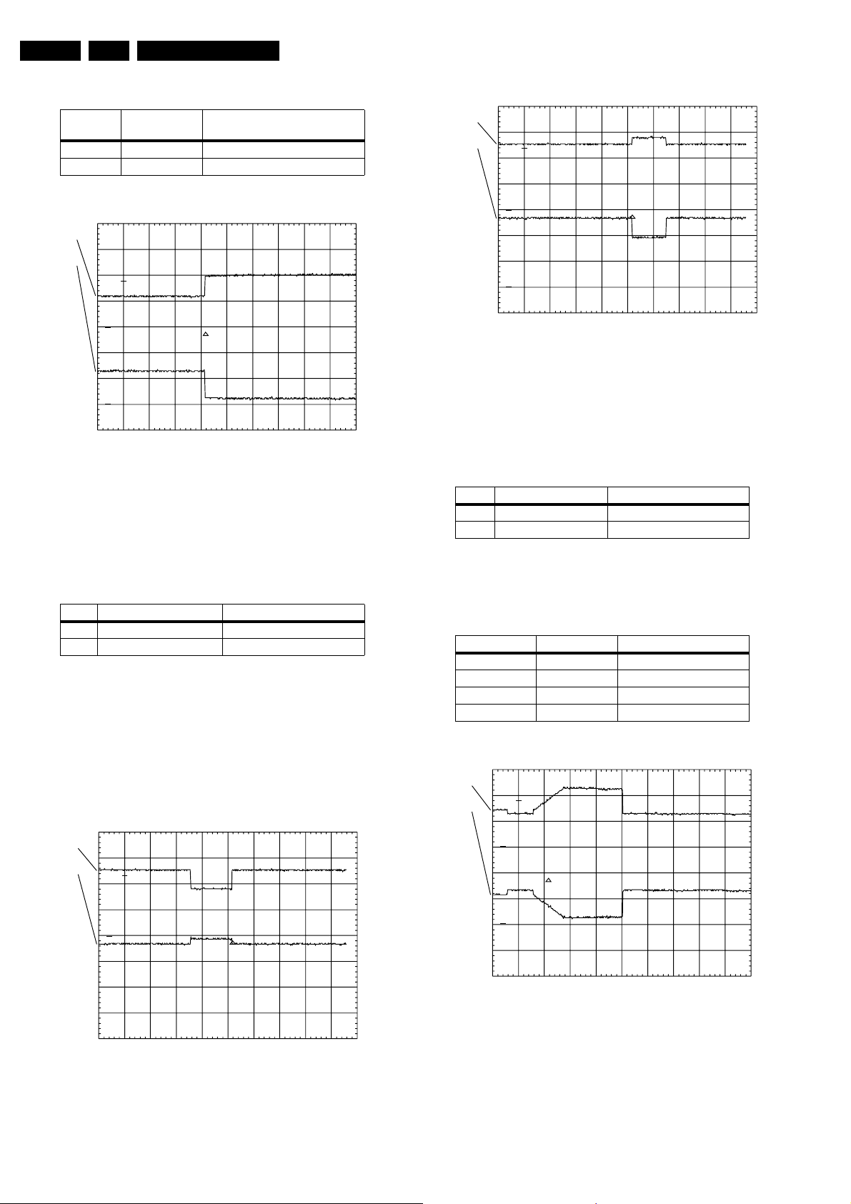
Table 5-23 Focus motor switching
Signal Name Testpoint Description
FOCUS - F005 Negative drive to focus coil
FOCUS + F006 Positive drive to focus coil
PM3380B
ch2
ch1
2
T
1
CH1 1.00V=
CH2 1.00V= MTB 500ms 4.08dv ch1+
Figure 5-33 Focus ON Command
5.6.7 Hf Path
CL 36532043_061.eps
030603
5.6.6 Focus check
Test need a DVD disc in the DVD player to operate properly.
The focus control circuit is checked using the following
commands:
Table 5-22 Focus check commands
Ref. # Command Name Remark
38a BeFocusOn Focus on
38b BefocusOff Focus off
Visual check on the laser,when Focus control ON, if the
laserlight is visible.
Once the check is completed,switch the focus control OFF
before executing next command.
To check the waveform of FOCUS- and FOCUS+,
connect a 10W / 0.25W resistor between FOCUS- and
FOCUS+ to serve as dummy load without connecting the
loader.
Play DVD Test Disc.
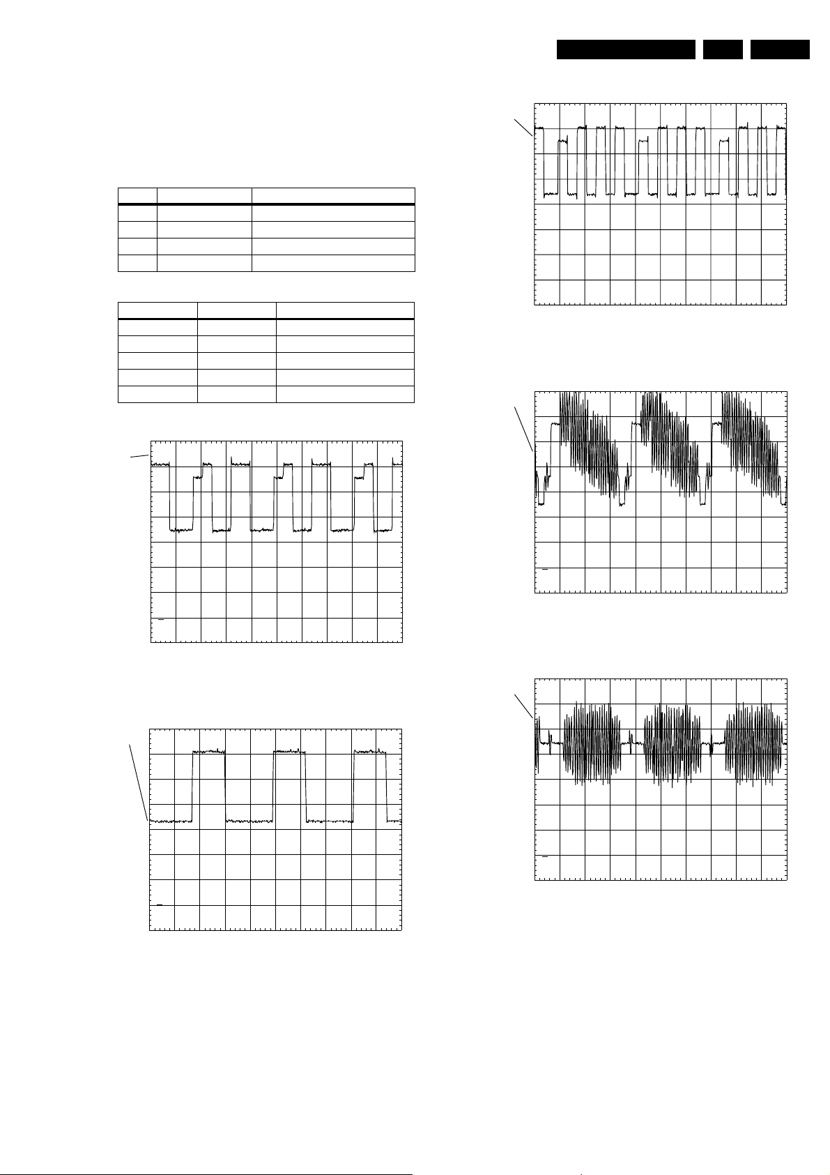
Measure outputs of diodes A, B, C, D, E, F.
Table 5-24
Signal Name Testpoint Value
A F016 2.5V +/-0.2%
B F015 2.5V +/-0.2%
C F014 2.5V +/-0.2%
D F017 2.5V +/-0.2%
E F019 2.5V +/-0.2%
F F018 2.5V +/-0.2%
At outputs of diodes A, B, C, D the following waveform can be
measured: Refer to Figure Output of diodes A, B, C, D
PM3380B
ch1
T
1
CH1 50.0mV= MTB 20.0us ch1+
CL 36532043_066.eps
030603
Figure 5-34 Output of diodes A,B,C,D
Check the HF output, RFO, at testland F219 and observe the
waveform, refer to Figure RFO.
Page 20
EN 20 SD-5.31SL5.
Test Instructions Mono Board SD5.31SL
PM3380B
ch1
1
CH1 1.00V= MTB 250ns ch1+
Figure 5-35 RFO
5.7 Diagnostic Software Description
5.7.1 Introduction
Purpose
This document describes all interfaces from the outside world
to the diagnostic software, what is needed to use these
interfaces and how to access them.
Scope
This document has been realised within the framework of the
DVD video player.
5.7.2 Definitions and Abbreviations
Definitions
Control PC Automatic test equipment, part of the
production control system in the
factory, to control the execution of
Diagnostic Nuclei in the DVD player.
Diagnostic Nucleus Part of the Diagnostic Software. Each
nucleus contains an atomic and
software independent diagnostic test,
testing a functional part of the DVD
player hardware on component level.
Script Part of the Diagnostic Software. Each
script contains a sequence of
Diagnostic Nuclei to be executed.
Service PC PC used by a service- or repair-person
to communicate with the Diagnostic
Software in the DVD player.
CL 36532043_068.eps
030603
Table 5-25 Interface overview
Logical
Interface Description
Menu
Interface
Menu-driven
activation of
individual nuclei,
used for Level 2/
Second Line
diagnostic mode.
Physical interface
components
- Service PC running a
terminal emulation
program, connected
to the RS232 port of
the DVD player.
- Test pin grounded
Users are service or
repair people
Command
Line
Interface
Used during Level 1
diagnostic mode.
Used to send
commands from the
Control PC into the
DVD hardware.
- Control PC, running a
control program (e.g.
Hyperterminal),
connected to RS232
port of the DVD
player.
- Test pin grounded
• In the next chapters the logical user interfaces are
described in more detail including the exact use of the
physical interface components.
5.9 Description of Interfaces
5.9.1 Menu Interface
The menu interface is part of the Level 2 / Second Line
diagnostic mode. Via the menu interface it is possible to control
the execution of the Diagnostic Nuclei.
Set-up Physical Interface Components
Hardware required:
• Service PC
• one free COM port on the Service PC
• special cable to connect DVD player to Service PC
The service PC must have a terminal emulation program (e.g.
OS2 WarpTerminal or Procomm /Windows Hyperterminal)
installed and must have a free COM port (e.g. COM1). Activate
the terminal emulation program and check that the port settings
for the free COM port are: 19200 bps, 8 data bits, no parity, 1
stop bit and no flow control. The free COM port must be
connected via a special cable to the RS232 port of the DVD
player. This special cable will also connect the test pin, which
is available on the connector, to ground (i.e. activate test pin).
Activation
Switch the player on and the following text will appear on the
screen of the terminal (program):
Abbreviations
FDS Full Diagnostic Software
5.8 Overview of Interfaces
The table below shows an overview of the user interfaces of the
Diagnostic Software. The table is based on logical interface,
interfaces as seen from user perspective. A logical interface
can use one or more physical interface components. The DVD
has only a single RS232 port, implying that all interfaces using
this port are mutually exclusive.
DVDv6 Diagnostic Software version 7.03 S
(M)enu, or (C)ommand [M]:@ m <enter>
Press ENTER to go to Main Menu
CC: >
CL 36532043_023.eps
020603
Figure 5-36
• The first line indicates that the Diagnostic software has
been activated and contains the version number of the
diagnostic; this is also an indication that the first basic
nucleus (nucleus number 1) has been executed
succesfully.
• The term "DVDv6" implies that the DSW is running in the
ZiVA5 platform (6th generation).Interpretation of the DSW
version is done as follows:
Page 21

Test Instructions Mono Board SD5.31SL
EN 21SD-5.31SL 5.
(X) Major revision number, always fixed to 7
(YY) Minor revision number, a two-digit number incremented for
every release of a DSW variant.
version X.YY Z
(Z) DSW variant ID letter, identifies the module/player where this
DSW was targeted to run:
A – SD5.11, I2C Master module-based players
B – SD5.2, I2C Master module, used in DVD760 players
C – SD5.2, I2C Master module, used in high-end SACD2003 players
D – SD5.12, I2C Slave module, used in MTV combi applications
S – SD5.31, I2C Slave module, used in MTV combi applications
CL 36532043_024.eps
220503
• The second line is the prompt asking the user to choose the
interface format. Enter ‘M’ to select Menu mode and the
main menu will appear.For the layout of the menus,
see chapter ‘Layout of Menu and Submenu’.
To switch between interfaces, the DVD player needs to be
switched off and on again.
Note: For player that has no Mechanical power switch, it can
be turned on by connecting the power-cable.
Usage
To select, type the number of the chosen menu-item at the
prompt. Each entry must be terminated with a ‘RETURN’.
Invalid selections will cause an error message by the Menu
Handler
Example:
Select > 99
Invalid menu choice, number out of range ER @
Press RETURN to continue @
CL 16532163_038.eps
230102
Result and output of an activated (and terminated) nucleus will
be sent back to the service terminal.
Example:
Select > 3
1301 OK @
Press RETURN to continue @
CL 36532043_025.eps
220503
After the user presses a key, the current menu is rebuilt on
screen.
Pressing “RETURN” at the prompt without any further input at
the terminal will always rebuild the main menu.
DVDv6 Diagnostic Software version 7.03 S
(M)enu, OR (C)ommand [M]:@ C <enter>
DD: >
CL 36532043_026.eps
220503
The first line indicates that the Diagnostic software has been
activated and contains the version number; this is also an
indication that the first basic nucleus (nucleus number 1) has
been executed succesfully. The second line lets the user
choose the interface format. Enter ‘C’ to select Command
Mode and the next three lines are the succesful result of the
two subsequent basic tests (nuclei 2, 4 and the detection of the
display type used by the panel respectively). If not all these
messages appear on the terminal screen, then the related
nucleus found an error. The last line is the prompt ("DD>"). The
diagnostic software is now ready to receive commands.
Note: For player that has no Mechanical power switch, it can
be turned on by connecting the power-cable.
Usage
The commands that can be given are the reference IDs of the
test nuclei. A command must be terminated with a <RETURN>
character from the control PC. When typing commands, the
backspace key can be used to make corrections.
In case of typing errors in the command, an error message is
returned.
Example:
DD: > CompSdarmWrR? (Nuclei name cannot be accepted)
0001 Unknown command ER @
DD: >
CL 16532163_041.eps
230102
If the command (the nucleus ID) is recognised, the nucleus is
executed. Result and output of an activated (and terminated)
nucleus will be sent back to the control PC according to the
standard layout.
Example for a command without error:
DD: > 13 <ENTER> (Execute PapAtapiEcho nuclei)
1300 OK @
DD: >
CL 36532043_027.eps
220503
Termination
The menu interface can be terminated by switching off the AC
power from the DVD player/ module.
5.9.2 Command Line Interface
The command line interface is part of level 1 diagnostic mode.
Via a command line interface the execution of Diagnostic
Nuclei can be controlled.
Set-up Physical Interface Components
Hardware required:
• Control PC
• one free COM port on the Control PC
• special cable to connect DVD player to the Control PC
The control PC must use the following port settings for the used
COM port: 19200 bps, 8 data bits, no parity, 1 stop bit and no
flow control. The control PC is connected with a special cable
to the RS232 port of the DVD player. Via the same connection
the test pin will be connected to ground.
Activation
After power on the next text will sent to the control PC
Example for a command with error:
DD: > 13 <ENTER>
1304 No response from ATAPI drive ER @
DD: >
CL 36532043_028.eps
220503
Termination
The command line interface is terminated by switching off the
AC power from the DVD player/ module.
5.10 Layout of Menu and Submenu
5.10.1 Layout Of Menus And Submenus For The Service Terminal
NOTE: a symbol “--” in the menu layouts indicates that that
specific menu choice will invoke the display of a submenu. This
symbol will also be used in the implementation of the menus
(i.e. the “--” will also appear in the user interface).
Page 22

EN 22 SD-5.31SL5.
Test Instructions Mono Board SD5.31SL
Menus
MAIN MENU
1 Audio...
2 Video...
3 Front Panel...
4 Basic Engine...
5 Processor Peripherals...
6 Error Log...
7 Miscellaneous...
First Level Submenus
MAIN > AUDIO MENU
1 Mute...
2 Pink Noise...
3 Sine Wave...
4 Digital Ports...
MAIN > VIDEO MENU
1 Colourbar...
2 Digital Port...
MAIN > FRONT PANEL MENU
1 No items available
MAIN > BASIC ENGINE MENU
1 Reset [44]
2 Version [37]
3 ATAPI...
4 Loader Mechanism...
5 Special Diagnostics...
MAIN > PROCESSOR PERIPHERALS MENU
1 Clock...
2 Flash...
3 NVRAM...
4 Processor info [5]
5 Slave IIC Loopback Test [90]
MAIN > ERROR LOG MENU
1 Read Last Errors [31]
2 Read Error Bits [32]
3 Reset Error Log [33]
MAIN > MISCELLANEOUS MENU
1 Statistics Info...
2 Read DVD Application version [46]
5 Set Video Out To RGB [61a]
6 Set Video Out To YUV [61b]
MAIN > VIDEO > DIGITAL PORT MENU
1 Video Port Out 0xAA [17a]
2 Video Port Out 0x55 [17b]
MAIN > BASIC ENGINE > ATAPI MENU
1 ATAPI Echo [13]
MAIN > BASIC ENGINE > MECHANISM MENU
1 Disc Motor...
2 Laser...
3 Tray...
4 Focus...
5 Radial...
6 Sledge...
7 Grooves...
MAIN > BASIC ENGINE > SPECIAL DIAGNOSTICS MENU
1 Read FlashID [70]
2 ROM Checksum [71]
3 Scratch Detector Test [72]
MAIN > PROCESSOR PERIPHERALS > PCM CLOCK MENU
1 PCM_CLK In CDDA Mode (11.3MHz) [8a]
2 PCM_CLK In DVD Mode (12.3MHz) [8b]
3 PCM_CLK In DVD96kHz Mode (24.6MHz) [8c]
MAIN > PROCESSOR PERIPHERALS > FLASH MENU
1 Verify FLASH Checksum [6]
2 Show FLASH Checksum [62]
3 FLASH Write Acces [10]
MAIN > PROCESSOR PERIPHERALS > NVRAM MENU
1 I2C NVRAM Acces [11]
2 NVRAM Config [34]
3 NVRAM Reset [35]
4 NVRAM Modify [36]
5 NVRAM Read/Wr Test [15]
MAIN > MISCELLANEOUS > STATISTICS INFO MENU
1 Total Nr Of Times Tray Open [47a]
2 Total Time Power On [47b]
3 Total Play-Time CDDA & VCD [47c]
4 Total Play-Time DVD [47d]
Third Level Submenus
Second Level Submenus
MAIN > AUDIO > MUTE MENU
1 Mute On [19a]
2 Mute Off [19b]
MAIN > AUDIO > PINK NOISE MENU
1 Pink Noise On [20a]
2 Pink Noise / Beep Tone Off [20b]
3 Beep Tone On [20c]
MAIN > AUDIO > SINE WAVE MENU
1 Audio Sine On [21a]
2 Audio Burst On [21b]
MAIN > AUDIO > DIGITAL PORTS MENU
1 No test available
MAIN > VIDEO > COLOURBAR MENU
1 Colourbar DENC On (PAL) [23a]
2 Colourbar DENC On (NTSC) [23c]
3 Colourbar DENC/MPEG Off [23b]
4 ProgressiveScan MPEG On [24a]
MAIN > BASIC ENGINE > MECHANISM > DISC MOTOR MENU
1 Disc Motor On [39a]
2 Disc Motor Off [39b]
MAIN > BASIC ENGINE > MECHANISM > LASER MENU
1 CD Laser On [58a]
2 CD Laser Off [58b]
3 DVD Laser On [58c]
4 DVD Laser Off [58d]
MAIN > BASIC ENGINE > MECHANISM > TRAY MENU
1 Tray Open [43b]
2 Tray Close [43a]
MAIN > BASIC ENGINE > MECHANISM > FOCUS MENU
1 Focus On [38a] (load DVD first)
2 Focus Off [38b]
MAIN > BASIC ENGINE > MECHANISM > RADIAL MENU
1 Radial Control On [40a] (load DVD first)
2 Radial Control Off [40b]
Page 23

Test Instructions Mono Board SD5.31SL
MAIN > BASIC ENGINE > MECHANISM > SLEDGE MENU
1 Sledge Inwards [41a]
2 Sledge Outwards [41b]
MAIN > BASIC ENGINE > MECHANISM > GROOVES (Uses DVD) MENU
1 Jump To Inside Grooves [42a]
2 Jump To Middle Grooves [42b]
3 Jump To Outside Grooves [42c]
1. 0001 Unknown command ER @
2. 3100 OK @
3. 0901 Data line X is not connected to the DRAM ER @
4. Device ID: 0x01
Manufac ID: 0xC2
7000 OK @
5.11 Diagnostic Nuclei
EN 23SD-5.31SL 5.
CL 16532163_045.eps
230102
Screen Layout With Menus
When menus are used, no specific screen layout can be given:
menu information will not be in a special format, except for the
layout as mentioned in the previous paragraphs.
A typical menu session can look as follows:
DVDv6 Diagnostic Software version 7.03 S
(M)enu, or (C)ommand [M]:@ <enter>
Press ENTER to go to main menu
CC: > <enter>
MAIN MENU
1. Audio ...
2. Video ...
3. Front Panel ...
4. Basic Engine ...
5. Processor Peripherals ...
6. Error Log ...
7. Miscellaneous ...
Select > 4 <enter>
MAIN > BASIC ENGINE MENU
1. Reset [44]
2. Version [37]
3. S2B
4. Loader Mechanism ...
5. Special Diagnostics ...
Press Enter to go to Main Menu
Select > 5 <enter>
MAIN > BASIC ENGINE > SPECIAL DIAGNOSTIC MENU
1. Read flashID [70]
2. ROM checksum [71]
3. Scratsh detector test [72]
Press Enter to go to Main Menu
CL 36532043_029.eps
020603
Each nucleus contains an atomic and independent diagnostic
test, testing a functional part of the DVD player hardware on
component level. Each Nucleus returns a result message to its
caller. Some tests (e.g. generating a colour bar) can only return
an "OK" result. Internal communication will be done via a
uniform interface between the diagnostic Engine, Scripts and
the Diagnostic Nuclei.
The diagnostic Engine can only operate if a certain (minimal)
set of hardware is functioning properly. To test this set of
hardware, a set of basic diagnostic nuclei is embedded in the
DVD player. Each basic diagnostic nucleus will only test that
part of the hardware which is required for execution of the
diagnostic Engine, e.g. a RAM test will only test that part of
RAM that is used by the diagnostic engine. After the Diagnostic
Engine is operational it is possible to do a full RAM diagnostic.
All basic diagnostic nuclei start with prefix 'Basic'.
In the overview each Diagnostic Nucleus consists of a
reference number, a reference name and remarks. Reference
number and name are coupled and one of them is enough for
unique identification.
Figure 5-37
Depending on the height of the screen, the text will start
scrolling off the top of the screen.
Layout Of Results Diagnostic Nuclei On Control/service Pc
Results returned from a Diagnostic Nucleus to the control/
service PC will have a maximum length of 300 characters and
are terminated by a CR character (included in the string length)
The result has the following layout
< number >< string > [OK l ER] @< CR >
The use of the "@" enables the Asterix system on the Control
PC to parse the output string of each nucleus into a database.
< number > is a 4-digit decimal number padded with leading
zeros if its value is less than 4 digits. The first two digits identify
the generating nucleus (or goup of nuclei), the latter two digits
indicate the error number.
< string > is a text string containing information about the result
of the Diagnostic Nucleus.
< number > and < string > are defined in [SDD_DN] in the
output sections of each Nucleus.
Examples:
Page 24

EN 24 SD-5.31SL5.
Test Instructions Mono Board SD5.31SL
Table 5-26 Basic diagnostic nuclei
Ref. # Reference Name Remark
1 BasicSpAcc Serial port Access test/
initialization
5 CompProcInfo Display processor specific
Table 5-27 Processor and peripherals
Ref. # Reference Name Remark
6 PapChksFl Calculate and Verify
7a PapUclkAclkCdda External uClock A_CLK in
7b PapUclkAclkDvd External uClock A_CLK in
7c PapUclkAclkDvd96 External uClock A_CLK in
8a PapSgsAclkCdda Internal PLL CLK in CD-DA
8b PapSgsAclkDvd Internal PLL CLK in DVD
8c PapSgsAclkDvd96 Internal PLL CLK in DVD
10 PapFlashWrAcc Tests Backend flash Write
11 PapI2cNvram I2C NVRAM access
12 PapI2cDisp I2C/Sio Bus-Display PWB
13 PapUdeEcho/
PapATAPIEcho
14 PapUdePass Enter UDE Pass-through
15 PapNvramWrR NVRAM Write Read
62 PapChksSum Show checksums stored in
info (LOR register,
Chip Revision)
Checksum FLASH
CD-DA mode (SD5.2only)
DVD mode (SD5.2 only)
DVD (96kHz)
mode (SD5.2 only)
mode
mode
mode
Access function
communication check
UDE Echo(SD5.2) / ATAPI
echo (SD5.12/SD5.31)
(SD5.2 only)
flash
19a AudioMuteOn Audio Mute On
67b DAC_ClockExternal Uses external clock for
68a DAC_AudioPreMuteOn Enable Audio Pre-mute
68b DAC_AudioPreMuteOff Disable Audio Pre-mute
69a DAC_CenterOn Enable Center on pin
69b DAC_CenterOff Disable Center on pin
79 DAC_Reset Resets DAC
80a DAC_ModeCDDA Sets DAC to CDDA
80b DAC_ModeDVD48 Sets DAC to DVD mode
80c DAC_ModeDVD96 Sets DAC to DVD mode
80d DAC_ModeDSD Sets DAC to DSD mode
81a DAC_LowPowerStandbyOnEnable Low Power
81b DAC_LowPowerStandby
Off
82a DAC_UpsamplingFreq192kSets Upsampling fre-
82b DAC_UpsamplingFreq96kSets Upsampling fre-
82c DAC_UpsamplingOn Enable upsampling
82d DAC_UpsamplingOff Disable upsampling
DAC (384fs)
pin
pin
mode
(48kHz)
(96kHz)
Standby
Disable Low Power
Standby
quency to 192kHz
quency to 96kHz
Table 5-28 Audio
Ref. # Reference Name Remark
19a AudioMuteOn Audio Mute On
19b AudioMuteOff Audio Mute Off
20a AudioPinkNoiseOn Audio Pinknoise On
20b AudioPinkNoiseOff Aud io Pinknoise (or beep
tone) Off
20c AudioBeepToneOn Audio Beep Tone On
21a AudioSineOn Audio Sine signal On/Off
21b AudioSineBurst Audio Sine signal Burst
Table 5-29 Audio DAC related (SD5.2 only)
19a AudioMuteOn Audio Mute On
65 DAC_I2C Resets DAC and check
66a DAC_I2CEnable Enable I2C communica-
66b DAC_I2CDisable Disable I2C communica-
67a DAC_ClockInternal Uses internal clock from
I2C communication with
DAC
tion to AV board
tion to AV board
monoboard for DAC
(256fs)
Page 25

Test Instructions Mono Board SD5.31SL
EN 25SD-5.31SL 5.
Table 5-30 Video
Ref. # Reference Name Remark
17a VidPortOutAA Output the value 0XAA at
the Digital Video Interface
Port (SD5.2 only)
17b VidPortOut55 Output the value 0X55 at the
Digital Video Interface Port
(SD5.2 only)
23a VideoColDencOnPAL Colourbar (PAL) DENC On
23b VideoColDencOff Colourbar DENC / Digital
Video Off
23c VideoColDencOnNTSCColourbar (NTSC) DENC
On
24a VideoProgMPEGon Progressive - DigitalVideo
Colour Bar ON
(SD5.2 only)
24b VideoYuvMPEGon Enhanced YUV-
DigitalVideo Colour Bar
25a VideoScartLo Scart Low (SD5.2 only)
25b VideoScartMi Scart Medium (SD5.2 only)
25c VideoScartHi Scart High (SD5.2 only)
54 VideoScartSwComm Scart Switch communication
(SD5.2 only)
55a VideoScartSwDvd Scart Switch Dvd
(SD5.2 only)
55b VideoScartSwPass Scart Switch Pass-through
(SD5.2 only)
57a VideoScartPinLo PIO-pins used for Scart-
switching
57b VideoScartPinMi PIO-pins used for Scart-
switching
57c VideoScartPinHi PIO-pins used for Scart-
switching
61a VideoColOutRGB Enable Video Output to
RGB
61b VideoColOutYUV Enable Video Output to
YUV
Ref. # Reference Name Remark
46 MiscApplVer Read version of
application software
47a MiscTrayOpenNr Read the number of
times the tray opened
47b MiscPowerOnTime Read the total time the
player's power has been
on
47c MiscPlayTimeCddaVcd Read the Playtime of
CDDA and VCD discs
47d MiscPlayTimeDvd Read the Playtime of
DVD discs
Table 5-31 Display (slave processor) (SD5.2 only)
Ref. # Reference Name Remark
26 DispVer Version number
27 DispKeyb Keyboard
28 DispRc Remote Control
29 DispLed LEDs
30a DispDisplay VFT Display test
30b DispLCDisplay LCD Display test
30c DispLCDBkLight LCD Backlight test
60 DispP50 P50 loopback test
Table 5-32 Log (Error logging in Nvram)
Ref. # Reference Name Remark
31 LogReadErr Read last Errors
32 LogReadBits Read errors Bits
33 LogReset Reset
Table 5-33 Miscellaneous
Ref. # Reference Name Remark
34 MiscReadConfig Read Configuration area
35 MiscNvramReset NVRAM Reset
36 MiscNvramMod Modify NVRAM contents
from NVRAM
Page 26

EN 26 SD-5.31SL5.
Test Instructions Mono Board SD5.31SL
Table 5-34 Basic engine
Ref. # Reference Name Remark
37 BeVer Version number
38a BeFocusOn Focus On
38b BeFocusOff Focus Off
39a BeDiscmotorOn Discmotor On
39b BeDiscmotorOff Discmotor Off
40a BeRadialOn Radial control On
40b BeRadialOff Radial control Off
41a BeSledgeIn Sledge Inwards
41b BeSledgeOut Sledge Outwards
42a BeGroovesIn jump Grooves to Inside
42b BeGroovesMid jump Grooves to Middle
42c BeGroovesOut jump Grooves to Outside
43a BeTrayIn Tray In
43b BeTrayOut Tray Out
44 BeReset Reset Basic Engine
58a LaserCdOn CD Laser on
58b LaserCdOff CD Laser off
58c LaserDvdOn DVD Laser on
58d LaserDvdOff DVD Laser off
70 BedReadFlashID Read flash memory manufac-
turer and device ID
71 BedCalcRomChk-
sum
72 BedScratchTest Test scratch detection circuit
Table 5-35 Furore IC (SD5.2 only)
Ref. # Reference Name Remark
62 Furore_SdramWrR Furore SDRAM Write Read
63 Furore_SdramWrR
Fast
64 Furore_Id Furore version ID check
83 Furore_Reset Furore reset
84a Furore_High Sets Furore output pins
84b Furore_Low Sets Furore output pins
Table 5-36 Karaoke (not available)
Ref. # Reference Name Remark
48a KaraokeModeOff Switch Karaoke mode off
48b KaraokeModeOn Switch Karaoke mode on
49 KaraokeMicInput Check path from the
50a KaraokeKeyOn Set Karaoke Key to the
50b KaraokeKeyOff Set Karaoke Key to flat octave
51a KaraokeEchoOn Set Echo Control fuction on
51b KaraokeEchoOff Set Echo Control function off
Calculate ROM checksum
test
Furore SDRAM interconnec-
tion test
DSD_PCM0-9 to high
DSD_PCM0-9 to low
microphone input to audio
output
maximum level (1200 cent)
(0 cent)
5.12 Nuclei Error Codes
In the following tables the error description of the error codes
will be described.
5.12.1 Audio Nuclei
Error
code
1800 Audio Deemp On OK
1820 Audio Deemp Off OK
1880 Audio Deemp Tri OK
1900 Audio mute On OK
1920 Audio mute Off OK
1940 Audio Front LR mute On OK
1960 Audio Front LR mute Off OK
2000 Audio Pinknosie On OK
2001 Audio Pinknoise On DAC fail
2020 Audio Pinknoise Off OK
2040 Audio Beep tone On OK
2041 Audio Beep tone On DAC fail
2100 Audio Sine On OK
2101 Audio Sine On DAC fail
2120 Audio Sine Burst OK
2121 Audio Sine Burst DAC fail
6600 DAC I2C OK
6601 DAC I2C Bus busy
6602 DAC I2C expander
6603 DAC I2C DAC 4362
6620 DAC I2C enable OK
6640 DAC I2C disable OK
6700 DAC Clk internal OK
6701 DAC Clk internal I2C bus busy
6702 DAC Clk internal I2C failed
6720 DAC Clk external OK
6721 DAC Clk external I2Cbus busy
6722 DAC Clk external I2C failed
6800 DAC Audio pre-mute On OK
6801 DAC Audio pre-mute On I2C bus busy
6802 DAC Audio pre-mute On I2C failed
6820 DAC Audio pre-mute Off OK
6821 DAC Audio pre-mute Off I2C bus busy
6822 DAC Audio pre-mute Off I2C failed
6900 DAC Center On OK
6901 DAC Center On I2C bus busy
6902 DAC Center On I2C failed
6920 DAC Center Off OK
6921 DAC Center Off I2C bus busy
6922 DAC Center Off I2C failed
7900 DAC Reset OK
7901 DAC Reset I2C bus busy
7902 DAC Reset I2C expander
8000 DAC Mode CDDA OK
8001 DAC Mode CDDA I2C bus busy
8002 DAC Mode CDDA I2C failed
8020 DAC Mode DVD48 OK
8021 DAC Mode DVD48 I2C bus busy
8022 DAC Mode DVD48 I2C failed
8040 DAC Mode DVD96 OK
8041 DAC Mode DVD96 I2C bus busy
8042 DAC Mode DVD96 I2C failed
8060 DAC Mode DSD OK
8061 DAC Mode DSD I2C bus busy
8062 DAC Mode DSD I2C failed
8100 DAC Low Power Standby On OK
8101 DAC Low Power Standby On I2C bus busy
8102 DAC Low Power Standby On I2C failed
Error text
Page 27

Test Instructions Mono Board SD5.31SL
EN 27SD-5.31SL 5.
Error
code
8120 DAC Low Power Standby Off OK
8121 DAC Low Power Standby Off I2C bus busy
8122 DAC Low Power Standby Off I2C failed
8200 DAC Upsample 192k OK
8201 DAC Upsample 192k I2C bus busy
8202 DAC Upsample 192k I2C failed
8220 DAC Upsample 96k OK
8221 DAC Upsample 96k I2C bus busy
8222 DAC Upsample 96k I2C failed
8240 DAC UpSample On OK
8241 DAC UpSample On bus busy
8242 DAC UpSample On I2C failed
8260 DAC UpSample Off OK
8261 DAC UpSample Off bus busy
8262 DAC UpSample Off I2C failed
5.12.2 Basic Engine Nuclei
Error
code Error text
3900 Test successful
3901 “Parity error from Basic Engine to Serial”
3902 “Unexpected response from Basic Engine”
3903 “Communication time-out error”
3904 “Basic Engine returned error number 0xXX”
3921 “Parity error from Basic Engine to Serial”
3922 “Unexpected response from Basic Engine”
3923 “Communication time-out error”
3924 “Basic Engine returned error number 0xXX”
3800 Test successful
3801 “Parity error from Basic Engine to Serial”
3802 “Unexpected response from Basic Engine”
3803 “Communication time-out error”
3804 “Basic Engine returned error number 0xXX”
3805 “Focus loop could not be closed”
3820 Test successful
3821 “Parity error from Basic Engine to Serial”
3822 “Unexpected response from Basic Engine”
3823 “Communication time-out error”
3824 “Basic Engine returned error number 0xXX”
4200 Test successful
4201 “Parity error from Basic Engine to Serial”
4202 “Unexpected response from Basic Engine”
4203 “Communication time-out error”
4204 “Basic Engine returned error number 0xXX”
4205 “Sledge could not be moved to home
4206 “Focus loop could not be closed”
4207 “Motor not on speed within time-out”
4208 “Radial loop could not be closed”
4209 “PLL could not lock in accessing or tracking
4210 “Subcode or sector information could not be
4211 “Requested subcode item could not be
4212 “TOC could not be read in time”
4213 “Seek could not be performed”
4220 Test successful
Error text
position”
state”
read”
found”
Error
code Error text
4221 “Parity error from Basic Engine to Serial”
4222 “Unexpected response from Basic Engine”
4223 “Communication time-out error”
4224 “Basic Engine returned error number 0xXX”
4225 “Sledge could not be moved to home
position”
4226 “Focus loop could not be closed”
4227 “Motor not on speed within time-out”
4228 “Radial loop could not be closed”
4229 “PLL could not lock in accessing or tracking
state”
4230 “Subcode or sector information could not be
read”
4231 “Requested subcode item could not be
found”
4232 “TOC could not be read in time”
4233 “Seek could not be performed”
4240 Test successful
4241 “Parity error from Basic Engine to Serial”
4242 “Unexpected response from Basic Engine”
4243 “Communication time-out error”
4244 “Basic Engine returned error number 0xXX”
4245 “Sledge could not be moved to home
position”
4246 “Focus loop could not be closed”
4247 “Motor not on speed within time-out”
4248 “Radial loop could not be closed”
4249 “PLL could not lock in accessing or tracking
state”
4250 “Subcode or sector information could not be
read”
4251 “Requested subcode item could not be
found”
4252 “TOC could not be read in time”
4253 “Seek could not be performed”
4000 Test successful
4001 “Parity error from Basic Engine to Serial”
4002 “Unexpected response from Basic Engine”
4003 “Communication time-out error”
4004 “Basic Engine returned error number 0xXX”
4005 “Radial loop could not be closed”
4020 Test successful
4021 “Parity error from Basic Engine to Serial”
4022 “Unexpected response from Basic Engine”
4023 “Communication time-out error”
4024 “Basic Engine returned error number 0xXX”
4400 Test successful
4401 Test successful
4100 Test successful
4101 “Parity error from Basic Engine to Serial”
4102 “Unexpected response from Basic Engine”
4103 “Communication time-out error”
4104 “Basic Engine returned error number XX”
4120 Test successful
4121 “Parity error from Basic Engine to Serial”
4122 “Unexpected response from Basic Engine”
4123 “Communication time-out error”
4124 “Basic Engine returned error number XX”
Page 28

EN 28 SD-5.31SL5.
Test Instructions Mono Board SD5.31SL
Error
code Error text
4300 Test successful
4301 “Parity error from Basic Engine to Serial”
4302 “Unexpected response from Basic Engine”
4303 “Communication time-out error”
4304 “Basic Engine returned error number 0xXX”
4320 Test successful
4321 “Parity error from Basic Engine to Serial”
4322 “Unexpected response from Basic Engine”
4323 “Communication time-out error”
4324 “Basic Engine returned error number 0xXX”
3700 “Version: X.Y.Z”
3701 “Parity error from Basic Engine to Serial”
3702 “Unexpected response from Basic Engine”
3703 “Communication time-out error”
3704 “Basic Engine returned error number 0xXX”
5800 Test successful
5820 Test successful
5840 Test successful
5860 Test successful
5801 "Unexpected response from Basic Engine"
7000 "Manuf. ID: <XX>" "Device ID: <YY>"
7001 "Comm Test Failed"
7002 "Load Cmd Failed"
7003 "Load Dat Failed"
7004 "Run Cmd Failed"
7100 "ROM Checksum: XXXX"
7101 "Comm Test Failed"
7102 "Load Cmd Failed"
7103 "Load Dat Failed"
7104 "Run Cmd Failed"
7201 "Comm Test Failed"
7200 "Test successful"
7202 "Load Cmd Failed"
7203 "Load Dat Failed"
7204 "Run Cmd Failed"
7205 "Scratch circuit not OK"
5.12.3 Display PWB Nuclei
Error
code Error text
3000 “Test successful”
3001 “Disp not responding”
3002 “Disp key no response”
3003 “One or more patterns not correct”
3004 “Disp type invalid”
3020 “Test successful”
3021 “Disp not responding”
3022 “Disp key no response”
3023 “One or more patterns not correct”
3040 “Test successful”
3041 “Disp not responding”
3042 “Disp key no response”
3043 “One or more patterns not correct”
2700 “Model name in wich the test is running”
2701 “Disp key no response”
2702 “Disp not responding”
Error
code Error text
2707 “Stop key not pressed”
2708 “Pause key not pressed”
2709 “Play key not pressed”
2710 “Open/close key not pressed”
2713 “Previous key not pressed”
2714 “Next key not pressed”
2715 “More than one key not pressed”
2716 " Audio key not pressed"
2900 “Test successful”
2901 “Slave not responding”
2902 “Slave keyboard not responding”
2903 “Standby led not working”
2800 “Test successful”
2801 “Slave display controller not responding”
2802 “Slave keyboard not responding”
2803 “No key press received from remote control”
2600 “The ROM version of the slave processor =
0xXX, and the internal ID = 0xYY”
2601 “I2c bus busy”
2602 “I2c bus not working“
6000 P50 test
6001 “No readback on P50”
6002 “Disp not responding “
6003 “P50 readback error”
5.12.4 Processor & Peripherals Nuclei
Error
code Error text
700 Test successful
720 Test successful
740 Test successful
600 "All checksums are correct"
601 “Following checksum is faulty: BootCode1
Checksum is 0xY2 and is not correct (must be
0xZ2)”
601 “This test is not available when stand-alone
compiled”
6200 "Checksums = 0xA1, 0xB1, 0xC1, 0xD1"
6201 “This test is not available when stand-alone
compiled”
1000 Test successful
1001 Test successful
1020 Test successful
1021 Test successful
1100 Test successful
1104 “NVRAM reply time-out”
1200 Test successful
1202 “Slave bus not working”
1203 “Slave controller not responding”
1204 “Slave response is not correct”
5900 Test successful
Page 29

Test Instructions Mono Board SD5.31SL
EN 29SD-5.31SL 5.
Error
code Error text
5901 “I2c bus busy”
5902 “I2c bus not working“
5904 “DTS chip response not correct”
1300 Test successful
1301 “Parity error from basic engine to serial”
1302 “Parity error from serial to basic engine”
1303 “No communication between serial and basic
engine”
1304 “Communication time-out error”
1600 Test successful
1601 “The DVD SDRAM is faulty”
5.12.5 Log Nuclei
Error
code Error text
3100 "Show error log"
3101 "Error log is invalid"
3102 "Error log could not be read from NVRAM"
3103 "I2C bus busy before start"
3200 "Show error bit"
3201 "Error log is invalid"
3202 "I2C bus busy before start"
3203 "Error log could not be read from NVRAM"
3300 "Error log is cleared"
3301 "Error log could not be cleared"
3302 "I2C bus busy before start"
5.12.6 Miscellaneous Nuclei
Error
code Error text
3400 Test successful
3401 “The configuration data could not be read
from NVRAM”
3402 “I2C bus busy before start”
3500 “NVRAM is cleared”
3501 “The NVRAM could not be reset.”
3502 “I2C bus busy before start”
Error
code Error text
5403 “Scart switch controller not responding”
5404 “Scart switch controller response not correct”
5500 Test successful
5501 “I2c bus busy”
5502 “I2c bus not working“
5520 Test successful
5521 “I2c bus busy”
5522 “I2c bus not working“
5523 “Scart switch controller not responding”
5200 Test successful
5201 “I2c bus busy”
5202 “I2c bus not working“
5300 Test successful
5301 “I2c bus busy”
5302 “I2c bus not working“
5320 Test successful
5321 “I2c bus busy”
5322 “I2c bus not working“
4700 “Number of times Tray went Open : XX”
4701 The total number of times tray went open
could not be read from NVRAM.
4702 I2C bus busy before start
4720 “Total Power On time (minutes) : XX”
4721 The total power-on time could not be read
from NVRAM.
4722 I2C bus busy before start
4740 “Total CDDA & VCD disks Play-time
(minutes) : XX”
4741 The playtime of CDDA & VCD disks could not
be read from NVRAM.
4742 I2C bus busy before start
4760 “Total DVD disks Play-time (minutes) : XX”
4761 The playtime of DVD disks could not be read
from NVRAM.
4762 I2C bus busy before start
4600 “Version of Application Software : XX”
4601 “The application version could not be read
from NVRAM.”
4602 “I2C bus busy before start”
3600 “NVRAM contents updated.”
“NVRAM contents and configuration
checksum updated.”
3601 “NVRAM contents could not be updated.”
3602 “I2C bus busy before start”
3603 “NVRAM contents could not be read”
3604 “NVRAM not accessible.”
3605 “NVRAM checksum could not be updated.”
1500 Test successful
1502 “NVRAM access time-out”
1504 “NVRAM fails”
5400 Test successful
5401 “I2c bus busy”
5402 “I2c bus not working“
5.12.7 Video Nuclei
Error
code
1700 Video digital port OK
1701 Video digital port failed
1720 Pscan IO exp OK
1721 Pscan IO exp com failed
2300 Video colourbar On OK
2301 Color Denc On transmit error
2302 I2C Color Denc On bus busy
2320 Video colourbar Off OK
2340 Video colourbar On NTSC OK
2400 ADV7300 com OK
2401 I2C ADV7300 com bus busy
2402 ADV7300 com transit error
Error text
Page 30

EN 30 SD-5.31SL5.
Test Instructions Mono Board SD5.31SL
Error
code
2403 No ack from ADV7300 com
2404 ADV7300 com response error
2420 FLI2200 com OK
2421 I2C FLI2200 com bus busy
2422 FLI2200 com transmit error
2423 No ack from FLI2200 com
2424 FLI2200 com response error
2460 Proscan com OK
2440 ADV7190 com OK
2441 I2C ADV7190 com bus busy
2442 ADV7190 com transmit error
2443 No ack from ADV7190 com
2444 ADV7190 com response response
2500 Video scart Low OK
2501 I2C Scart Low bus busy
2502 Scart Low transmit error
2520 Video scart Mid OK
2521 I2C Scart Mid bua busy
2522 Scart Mid transmit error
2540 Video scart High OK
2541 I2C Scart High bus busy
2542 Scart High transmit error
6100 Video colour RGB OK
6120 Video colour YUV OK
Error text
5.12.8 Furore Nuclei
Error
code
6300 Furore Sdram WRR_L OK
6301 Furore Sdram WRR_L DB fail
6302 Furore Sdram WRR_L AB fail
6303 Furore Sdram WRR_L DVC fail
6320 Furore Sdram WRR_H OK
6321 Furore Sdram WRR_H DB fail
6322 Furore Sdram WRR_H AB fail
6323 Furore Sdram WRR_H DVC fail
6400 Furore Sdram WRR_F_L OK
6401 Furore Sdram WRR_F_L DB fail
6402 Furore Sdram WRR_F_L AB fail
6403 Furore Sdram WRR_F_L DVC fail
6420 Furore Sdram WRR_F_H OK
6421 Furore Sdram WRR_F_H DB fail
6422 Furore Sdram WRR_F_H AB fail
6423 Furore Sdram WRR_F_H DVC fail
6500 Furore ID OK
6501 Furore ID invalid
8300 Furore reset OK
8301 Furore reset ID NOK
8400 Furore High OK
8420 Furore Low OK
Error text
Page 31

Block Diagram and Testpoint Overview Bare Board
T
[
]
[
]
3
[
]
[
]
]
Q
Q
]
p
h
7
3
3
3
3
K
Q
[
]
[
]
p
gDig
K
K
[
K
)
[
]
K
(
)
g
y
t
H
p
R
K
N
R
G
R
T
A
O
O
A
(
)
31SD-5.31SL 6.
6. Block Diagram and Testpoint Overview Bare Board
Block Diagram
SD5.31 BLOCK DIAGRAM
OUTSW
INSW HOMESW
connector Motor connector
Tra
1 LD- 1 SL2 LD+ Slo
3 OUTSW connector connector 3 GND
4 GND 4 HOMESW
5 INSW 5H+
LD+ SL + H2+ A2 10 H2+
LD- SL- H2- A3 11 H1-
TR+
TR- Servo driver S
FO+ BA5954FP BA6849FP
FO-
OPU connector
1 TR- MVREF2
2 TR+
3 FO4 FO+ SFOCUS SMOTO
5 PDDVD STRAC
6 VCC TRAYSW SFGI
7V
8 GND VC21 DRVSB
9 LDDVD VC25
10 LDCD
11 V
12 GND MEVO
13 PDCD
14 GND Laser control CEI
15 RFOU
16 C TEI
17 B TEXI MA[0:15] A16
18
19 D
20 F SEFGC MPSEN
21 E MIRR MWR
22 VCC SLDC
23 VS SP-3721
24 GND DVDMDI SCS
OPU
connector
DVDLD DVDLD
CDLD CDLD
VC21
CDMDI SDATA
A RD[0:15]
B RRAS
C RFO RCAS
D RWE
E ROE
F
RFOUT
MC34072
PIN
PI
RFRP SSLE
FEI
SDFCT MD[0:7]
SBAD MFSCS
SCLK
Power-on
Reset
ATAPI connector
for PCMCIA interface
From Back-end Host
Motor 2 SL+
H1+ 8 H3+
H1- A1 9 H2-
H3+ V
H3- 13 A1
indle motor driver
SSPDON
SB
ALi
M5705
UPA[1:3]
UPD[0:15]
HDMARQ
LDS
UDS
HDTACKn
HDMACK
ATAPIINTn
IDECS0n
IDECS1n
ATAPIRSTn
Clock
circuit
6H7H3-
12 H1+
14 A2
15 A3
RA[0:11]
Flash / ROM
M29F002BT
EDO DRAM
256K x 16
SOJ40
KAS161622D
Two SDRAM configuration option
2x TSOP54 SDRAM
2pcs x 1M x 16 x 4 = 128Mbits
Ext I2S Input
Digital
audio SPDIF - I2S
SPDIF conv.
Input
Module interface bus
1M x 16 M29W160
Flash / ROM
2M Bytes
TSOP48
UPA
1:22
UPD
0:15
SYSRSTn D D3 11 12 DD12 connector UPA2 7 8 UPA
UDS DD2 13 14 DD13 UPA15 9 10 UPA1
FLASHCSn DD1 15 16 DD14 UPA13 11 12 UPD14
Trans
arent latc
74HCT57
74HCT57
74HCT57
1:3
UPA
0:15
UPD
ALE
MA[0:11]
BA[0:1]
MD[0:31]
MCS0n
MRASn Clock
MCASn SDRAM interface circuit
MWEn
MCLK
MDQM[0:3]
MCS1n
Audio I2S input
XCLK
BCLK
LRCLK
Host interface ATAPI
MUX
GPIO I2C I2C Analo
(misc) Master Slave video audio BC L
GPIO MSCL SCL VD AC
MSDA SDA ADATA
MSCL
MSDA
64kbits
NVRAM
ATAPI connector
1 2 GND
RESE
DD7 3 4 DD8 ZK5 E-LINK connector
DD6 5 6 DD9
DD5 7 8 DD10 MEDUSACSn 3 4 +5V
DD4 9 10 DD11 ZK5 E-LINK ALE 5 6 SYSRSTn
DD0 17 18 DD15 UPA
GND 19 20 NC UPD
DMAR
21 22 GND HDMAR
DIOWn 23 24 GND LDS ALE UPD6 19 20 UPD
DIORn 25 26 GND UDS SYSRSTn U PD421 22 UPD5
IORDYn 27 28 NC HDTACKn HDTACKn UPD2 23 24 UPD
DMACK29 30 GND HDMAC
31 32 NC ATAPIINTn UDS MEDUSAINTn 27 28 DTACKn
INTR
DA1 33 34 NC IDECS0n LDS LDS 29 30 UDS
DA0 35 36 DA2 IDECS1n RWn RWn 31 32 GND
CS0n 37 38 CS1n ATAPIRSTn MEDUSACSn
NC 39 40 GND
ATAPI connector
1:3
0:15
UPA[1:3
UPD[0:15
MEDUSAINTn UPD0 25 26 UPD1
E-LINK
LSI Logic
Ziva5+
ut Microphone
Audio I2S out
ital XCL
I2C TXD1 TMS
INT. CTS1 TC
0:4]SPDIFLRCL
DAC
2/6 Ch
Analo
Service and JTAG bus Digital Input
diagnostic port TRSTvideo
RTS1 TDOVDATA(0:7
0:3
RXD1 TDI ITUT-656
Audio Out
GND 1 2 + 5V
UPA11 13 14 UPD12
UPA9 15 16 UPD10
UPD8 17 18 GND
SYSRSTn Reset
I2S KOK
circuit
A-D
Front-End Engine
Front-End Engine
CL 36532043_043.eps
030603
Page 32

Block Diagram and Testpoint Overview Bare Board
Testpoint Overview Bare Board
32SD-5.31SL 6.
3139 243 3063.4
CL 36532043_034.eps
020603
F001 B3
F002 A3
F003 C3
F004 C2
F005 D3
F006 C2
F007 B3
F008 C3
F009 C3
F010 A3
F011 B2
F012 C3
F013 B3
F014 B3
F015 B3
F016 B3
F017 B3
F018 C3
F019 C3
F020 A2
F021 B3
F022 B2
F023 C3
F024 B2
F101 D2
F102 D2
F103 D2
F104 D2
F105 D2
F106 D3
F107 D3
F108 D3
F109 D3
F110 D3
F111 D2
F112 D2
F113 D2
F114 D2
F115 D2
F116 A2
F117 A2
F118 A1
F119 A1
F120 A2
F121 A2
F122 A2
F123 B3
F124 D4
F201 C3
F203 D1
F204 C1
F205 B2
F206 C2
F209 C2
F211 B2
F212 B2
F213 B1
F217 C2
F218 C2
F219 B2
F220 C1
F401 B3
F402 C1
F413 A2
F414 A2
F415 A2
F416 A2
F417 A2
F418 A1
F419 C3
F420 D4
F421 B4
F422 B1
F424 B2
F425 B2
F431 D4
F432 D4
F434 B3
F501 C1
F502 D2
F503 D3
F601 B3
F602 B4
F603 C4
F604 B3
F605 B3
F606 B4
F607 B4
F608 B4
F609 B4
F611 B4
F612 B4
F613 A4
F614 A4
F615 A4
F617 B2
F618 B3
F619 C3
F621 B4
F622 B4
F623 B4
F706 A3
F707 A2
F708 A2
F709 C2
F710 A2
F801 C4
F802 C3
F803 C3
F804 C3
F805 C3
F806 C3
F807 C4
F808 C4
F809 C4
F810 C4
F811 C4
F812 A4
F813 C4
F814 B3
F815 C4
F816 C4
F817 C4
F818 C4
F819 C4
F820 C4
F821 C4
F822 C4
F823 B4
F824 B4
F825 B4
F826 A4
F827 B4
F828 B2
F829 A4
F830 D3
F831 D4
F832 C4
Page 33

Electrical Diagrams and PWB’s
7. Electrical Diagrams and PWB’s
Bare Board: DVD Analog Front-end
12
34567891011
DVD analog Front-end
A
22R
3000
3002
2SB1132
7000
B
C
22R
3004
3015
2SB1132
7001
D
E
F
G
H
*RESERVE
V
I
DC vtg measured in STOP-mode
1001
F003
1
F004
2
F005
3
F006
4
F007
5
F008
6
F009
7
8
F010
9
F011
10
F023
11
12
F012
13
14
F013
15
F014
16
F015
17
F016
18
F017
19
TO/FROM SLOT LOADER OPU
F018
20
F019
21
22
F020
23
F021
24
GND
5VRF
22R
5V
16V
2002
22u
3001
5V
1n0
BAS316
GND
5K1
2005
5000
10u
6000
5VRF
22R
2009
5V
100u 16V
1n0
2015
6001
BAS316
GND
TRACK-
TRACK+
FOCUS-
FOCUS+
DVDMDI
DVDLD
CDLD
CDMDI
PUHRF
VCI25
1u0
2035
10V
GND
C
D
3005
1K0
B
A
F
E
5001
10u
2004
2026
10V1u0
GND
M2
M2
M2
M2
M1
100n
M1
M1
M1
M1
M1
M1
M1
M1
M1
M1
M1
5V
3011
1K2
3014
470R
GND
F001
F002
5VRF
2025
GND
CDLDO
CDLD
DVDLDO
DVDLD
16V
100u
33SD-5.31SL 7.
12
5VRF
16V100u
100n
3V
56
BYP
2032
2007
0V6
55
RX
MEVO35MIN
34
2001
GND
3003
3V4
GND
8K2
54
DIN
2011
100n
2012
100n
5VRF
100n
2022
GND
4n7
47n
1n0
2027
GND
3020
4K7
4n7
GND
3016
470K
10K
3017
2018
5VRF
2043
470n
2017
33p
GND
2019
33p
2023
33p
M3
SCSJ
M3
SDATA
M3
SCLK
M3
SAE
M3
FEI
TEI
M3
MEI
M1
TEI
MEI
SDFCT
SBAD
RFRP
F022
M1
M1
M3
M3
M3
4000
+5V_1
2034
7003-B
5
8
1V8
1V8
MC34072
7
2036
2V
4
GND
56K3018
33p
6
SDEN
SD ATA
SCLK
5VRF
FNN
MEV
PI
36
DIP
FNP
NC5
NC4
NC3
NC2
LCP
LCN
MEI
TPH
53
3V4
52
2V3
51
2V3
50
49
32
31
48
47
46
45
44
43
CE
42
FE
41
TE
40
39
38
DFT
37
GND
5V
2V4
0V
0V
3V
2024
4V
4V
2V
2V
2V
2V3
2V5
2029
2V7
100n
3V5
2V2
F024
2041
MEI
M1
M1
MVREF2
M1
M1
M1
M1
M3
M1
M1
M1
M1
M1
M1
M1
M1
M1,M2
RFO
PUHRF
D
C
B
A
F
E
VCI25
MVREF2
GND
MC34072
2042
VPB
28
100n
GND
3V4
6061
AIP
5V
58
VPA
MRR
30MP29
2V53V1V8
2040
2V8
57
SIGO
150p
2033
1n0
5VRF
100n
MLPF
33
680p
10K
3019
1
2V1
100n
2028
7003-A
7002
SP3721A
2008
2010
680p
100n
GND
2013
2014
680p
2016
680p
680p
2020
680p
3006
1K2
3007
1K2
3008
10K
+5V
+5V_1
5002
8
4
GND
GND
8K2
100n2030
3012
3
2
3013
2V1
2V1
1K5
3009
10K
2037
2021
100p
16V100u
GND
100n
GND
2038
3V4
3V4
2V5
3V4
3V4
3V4
3V4
3V4
3V4
2V5
2V5
2V5
2V5
2V5
2V5
4V2
2V5
0V
1
2
3
4
5
6
7
8
9
10
11
12
13
14
15
16
17
18
19
20
21
DVDMDI
M1
DVDRFP
DVDRFN
PD1
PD2
A2
B2
C2
D3
CP
CN
D
C
B
A
F
E
CDTE
VCI2
NC
VNB
DVDPD
DVDLD
22
DVDLDO
M1
CDPD
23
0V5V5V
CDMDI
M1
3V4
64
CDRDDC
CDLD
24
3V
SLDC
CDLDO
M1
M3
CDRF
LDON
2003
100n
2006
100n
3V4
3V6
3V6
62
63
25
ATO P
26VC27
2V5
59
AIN
ATO N
VCI
2V1
5VRF
2039
100u 16V
1001 E1
2001 A10
2002 A3
2003 B9
2004 H3
2005 B3
2006 B9
2007 B9
2008 C7
2009 C3
A
2010 C7
2011 C11
2012 C11
2013 D7
2014 D6
2015 D3
2016 D7
2017 D11
2018 D11
2019 D11
2020 D6
2021 D7
B
2022 D11
2023 D11
2024 E10
2025 F4
2026 F3
2027 F11
2028 F6
2029 F10
2030 F6
2032 G9
2033 H9
2034 H11
C
2035 H3
2036 H12
2037 G7
2038 G7
2039 I8
2040 I9
2041 A9
2042 A6
2043 G11
3000 A2
3001 B3
D
3002 A2
3003 B10
3004 C2
3005 D3
3006 E6
3007 E6
3008 E6
3009 E7
3011 F2
3012 F6
3013 F6
3014 F2
E
3015 C2
3016 H11
3017 H11
3018 H12
3019 B5
3020 G11
4000 F12
5000 B3
5001 D3
5002 F6
6000 B3
6001 D3
F
7000 B2
7001 D2
7002 C8
7003-A F6
7003-B H12
F001 B4
F002 D4
F003 E2
F004 E2
F005 E2
F006 E2
G
F007 F2
F008 F2
F009 F2
F010 F2
F011 F2
F012 G2
F013 G2
F014 G2
F015 G2
F016 G2
F017 H2
F018 H2
H
F019 H2
F020 H2
F021 H2
F022 H12
F023 F2
F024 H10
I
BARE BOARD : 3139 243 3063.4
123456789101112
CL 36532043_035.eps
270503
Page 34

Electrical Diagrams and PWB’s
Bare Board: Spindle/Servo Motor Driver
12
Spindle / Servo motor driver
A
B
C
D
E
F
G
H
SFW-15R
1100
F101
1
F102
2
F103
3
F104
4
5
F106
6
F107
7
F108
8
F109
9
F110
10
F111
11
F112
PH-S
12
MOTOR
1101
2120
F113
13
F114
14
F115
15
F116
1
F117
2
1n0
1n0
2121
SPINDLE / SLEDGE
TO / FROM LOADER
TO LOADER
GND
1102
PH-S
F118
1
F119
2
3
F120
4
TO LOADER
1n0
1n0
2116
2115
GND
1103
PH-S
TO LOADER
1
2
3
2118
F121
F122
1n0
2119
GND
3125
220R
5101
5102
5103
5104
2117
1n0
GND
5106
5107
GND
F105
3100
1n0
GND
HOMESW
M5V
+3.3V
68R
3106
220R
5105
+5VSTBY
47K
47K
3116
SLOT_IN_DET
SLED-
SLED+
LOAD+
LOAD-
+5VSTBY
3105
+3.3V
3117
OUTSW
VH
H3-
H3+
H2-
H2+
H1-
H1+
DA1
DA2
DA3
68R
INSW
34SD-5.31SL 7.
3456789
M2
M2
M3
M2
M2
M2
M2
M2
M2
M8,M3
M2
M2
M2
M2
M2
M2
DA3
M2
M3
M3
DA2
M2
DA1
M2
H1+
M2
M2
M2
M2
M2
M2
H1-
H2+
H2-
H3+
H3-
2100 100n
100n2110
2112
100n
GND
7101
BA6849FP
RINF
28
A3
2
1V
A2
4
1V
A1
7
1V
GND
8
H1+
9
5V
H1-
10
5V
H2+
11
5V
H2-
12
5V
H3+
13
5V
H3-
14
5V
NC1
NC23NC3
NC416NC5
NC6
MT129MT2
56
19
301
VM1
VM2
VCC
ECR
CINF
11V
27
11V
26
11V
25
5V
FG
24
5V
23
PS
0V
EC
22
2V1
21
2V1
FR
20
GND
SB
18
17
0V
15
VH
5V
F124
2111
100n
100n
GND
2114
+5V
3118
33R
100K
3102
1R0
3104
1R0
3107
1R0
3124
M5V
F123
4105
SSPDON
SMOTOR
MVREF2
3121
220R
5100
SFGIN
GND
1u0
GND
VH
M9V
2106
M5V
4102
4107
4n7
6100
3101
33K
0R
2107
100p
3109
12K
3K3
3113
2108
2109
100p
4108
0R
3120
33K
3123
22K
BAS316
SFOCUS
M3
3108
MVREF2
M1
M3
M2
M3
M2
M3
M3
M3
M1
M3
M2
GND
M3
SSLEG
FOCUS-
TRACK-
TRAYSW
STRACK
DRVSB
2113
100n
M5V
33R
3111
10K
3122
33K
10 11 12 13
2102
PGND1
PreGND
22
M5V
8
VCC
GND
100n
2103
GND
GND
921
PVCC2
PVCC1
MT130MT2
29
2104
16V10u
100n
VOSL-
VOSL+
VOFC-
VOFC+
VOTK+
VOTK-
VOLD+
VOLD-
2105
11
5V2
12
5V2
13
2V5
14
2V5
15
2V5
16
2V5
17
2V5
18
2V5
1R03110
3112 1R0
3114 1R0
3115
1R0
7100
BA5954FP
2V1
2V5
2V5
2V1
2V1
2V1
2V5
20
2V5
2V1
24
2V5
25
2V5
26
2V1
27
2V1
28
2V5
23
1
2
3
4
5
6
7
VINFC
CFCerr1
CFCerr2
VINSL+
VINSL-
VOSL
VNFFC
VNFTK
VINLD
CTKerr2
CTKerr1
VINTK
BIAS
STBY
2101
GND
M9V_1
100n
10u 16V
PGND
10 19
SLED-
SLED+
FOCUS-
FOCUS+
TRACK+
TRACK-
LOAD+
LOAD-
M1,M2
M1,M2
1100 A1
1101 D1
1102 E1
1103 F1
2100 F4
2101 D10
2102 D11
2103 D11
2104 D12
2105 D12
2106 D8
2107 E10
2108 E9
A
2109 F10
2110 F4
2111 F7
2112 G4
2113 G9
2114 H7
2115 F1
2116 F2
2117 F2
2118 G1
2119 G2
2120 D1
B
2121 D2
3100 E2
3101 D10
3102 D7
3104 D7
3105 E2
3106 E2
3107 E7
3108 E9
3109 E10
3110 E13
C
3111 E9
3112 E13
3113 E10
3114 F13
3115 F13
3116 F2
3117 F2
3118 F7
3120 G10
3121 G7
3122 G9
3123 G10
D
3124 H7
3125 B2
4102 F9
4105 G7
M2
M2
M1
M1
M2
M2
4107 D9
4108 F10
5100 C8
5101 D2
5102 D2
5103 E2
5104 E2
5105 E2
E
5106 F2
5107 F2
6100 G9
7100 D10
7101 D5
F101 A2
F102 A2
F103 B2
F104 B2
F105 B2
F106 B2
F
F107 B2
F108 B2
F109 B2
F110 C2
F111 C2
F112 C2
F113 C2
F114 C2
F115 C2
F116 D2
F117 D2
F118 E2
G
F119 E2
F120 E2
F121 F2
F122 F2
F123 F7
F124 H6
H
*RESERVE
V
DC vtg measured in STOP-mode
BARE BOARD : 3139 243 3063.4
1234567
CL 36532043_036.eps
89101112
270503
13
Page 35

Electrical Diagrams and PWB’s
Bare Board: DVD Front-end Processor
123 7891011 12 13
DVD Front-end Processor
A
B
5202
F203
+5V
2211
C
M1
RFO
2225
3200
20K
GND
47n
470p
470p
2227
2226
GND
M2
D
E
F
TRAYSW
SFOCUS
M2
STRACK
M2
SSLEG
M2
SMOTOR
M2
47n
RFRP
M1
MVREF2
M1
TEXI
M1
TEI
M1
FEI
M1
G
H
I
*RESERVE
V
DC vtg measured in STOP-mode
BARE BOARD : 3139 243 3063.4
123
16V100u
6n8
2228
1u0 50V
6202
100n
+5V
2224
2237
BAS316
5VRF
2212
3240
22K
100n
GND
3220
5VPLL
5200
16V100u
2200
GND
+3.3V
F201
2213
100n
2214
F205
51K
3224
3K3
3225
3K3
3226
3K3
3227
10K
3233
33R
3235
1K5
3236
4K7
1n0
2233
GND
+5V
3238
7203
4V
BC847B
0V
22K
3242
GND
100n
1n0
4K7
2203
5203
100n
GND
2234
6201
50V1u0
1n0
3.3V_ALI
2215
47K
2230
2235
BAS316
2238
GND
3239
1K0
3229
35SD-5.31SL 7.
456
+5V
VCC5_FEM
5201
RAM ADDR LINES AND M5705 HARDWARE SETTING
7201
6
16
17
18
19
22
23
24
25
26
14
29
28
13
27
11
12
15
3243
A0
A1
A2
A3
A4
A5
A6
A7
A8
RAS_
LCAS_
UCAS_
WE_
OE_
NC1
NC2
NC3
M29F002BT
12
1V5
11
1V7
10
1V7
1V7
1V7
1V5
1V9
2V3
27
2V3
26
0V2
23
1V9
25
2V1
2V1
28
1V9
29
1V7
0V7
2V5
30
10K
10K
3247
1
VCC2
VCC3
VSS135VSS240VSS3
21
GND
DATA LINES
+5V
7202
A0
A1
A2
9
A3
8
A4
7
A5
6
A6
5
A7
A8
A9
A10
A11
4
RP_NC
A12
A13
A14
3
A15
2
A16
A17
GND
MSM514265E
RA(8)
0V
0V
3V
3V
0V5
0V5
0V5
0V5
0V5
0V5
0V5
0V5
0V5
0V5
0V5
0V5
0V5
0V5
0V5
0V5
0V
0V
0V
0V
0V
0V
0V
0V
0V
0V
0V
0V
0V
0V
0V
0V
0V
3V
3V
3V
2V3
0V
0V5
0V
3.3V_ALI
2223
1n0
GND
GND
3.3V_ALI
GND
RA(9)
3.3V_ALI
GND
XHD(10)
XHD(11)
XHD(12)
XHD(13)
XHD(14)
XHD(15)
HDACKJ
HCS16J
HPDIAGJ
GND
XHD(7)
XHD(8)
XHD(6)
XHD(9)
XHD(5)
XHD(4)
XHD(3)
XHD(2)
XHD(1)
XHD(0)
HDRQ
IOWJ
IORJ
IORDY
HINTJ
HA1
HA0
HA2
HCS1J
HCS3J
HDASPJ
3245
2K2
3218-133R
3218-2
3218-4
33R
33R3218-3
33R
RD(7)
RD(8)
RD(6)
RD(9)
RD(5)
RD(10)
RD(4)
RD(11)
RD(3)
RD(12)
RD(2)
RD(13)
RD(1)
RD(14)
RD(0)
RD(15)
MWRJ
2205
100n
100n
2206
100n
2217
100n
2219
100n
2218
2220
F219
100n
100n
100n
2216
100u 16V
F204
2221
2222
GND
1n0
4203
GND
5VRF
3.3V_ALI
5VRF
GND
100n
2232
F206
M1
M1
M1
M1
M1
M1
M2
M2
M2
M2
M2
M2
M2
M3
M1
M7
M3
M3
GND
SAE
SBAD
GND
SDFCT
SCSJ
SCLK
SD ATA
DRVSB
SFGIN
SSPDON
SLOT_IN_DET
HOMESW
OUTSW
INSW
MFSCSJ
SLDC
IDERST
MPSENJ
A16
2239
22p
2241
22p
GND
3234
3228 33R
3231
3232
+5V
3.3V_ALI
33M8688
CX-11F
5K1
33R
33R
F220
1205
GND
10K3248
100K
5VRF
3244
4K7
EJECT
100n
2V1
2V1
2V1
2V1
2V
2V1
2V1
2V
2V
2V
2V1
2V2
3V5
0V
3V
0V
3V
5V
0V
2V4
2V4
3V
0V
0V
3V
3V
3V7
1V6
2V5
1V5
47p
5K1
2207
2208
3204
1V6
7200
3216
M5705
1
AVSS_DS
2
2V1
XSRFIN
XSIPIN
AVDD5_DS
XSDSSLV
XSRSLINT
VDD
XSAWRC
XSRFGC
XSEFGC
XSFOCUS
XSTRACK
XSSLEG
AVDD5_DA
XSMOTOR
AVSS_DA
XSRFRPLP
XSTELP
XSVREF2
XSRFRP
XSTEXI
AVSS_AD
XSTEI
XSFEI
XSAEI
AVDAVDD5_AD
XSSBAD
GND
XSDFCT
XSCSJ
XSCLK
XS DATA
XSLDC
XSFGIN
XSSPDON
XSFLAG3
XSFLAG2
XSFLAG1
XSFLAG0
XMP1_7
XMP1_6
GND1
NC
XMP1_4
XMP1_3
XMFSCSJ
XMP1_2
XGFIO2
XMP1_1
XHRSTJ
XGPIO1
XGPIO0
XCRSTJ
XMPSENJ
VDD1
XMALE
XMP1_0
VDD2
XOSC1
XOSC2
1V5
GND
XSAWRCVCO
XMD0
GND2
60
62
61
1V
1V31V0V6
MD(0)
MD(1)
3
0V
4
5
0V
6
2V1
7
8
1V6
9
2V1
10
11
12
13
14
15
16
17
18
19
20
21
22
23
24
25
26
27
28
29
30
31
32
33
34
35
36
37
38
39
40
41
42
43
44
45
46
47
48
49
50
51
52
53
54
55
56
57
58
59
F209
47n
10K
560p
2209
3205
1V8
2V1
2V1
2V1
175
173
172
174
176
XSVREFO
XSFTROPI
XSVR_PLL
XSPDOFTR2
XMD164XMD265XMD366XMD467XMD568XMD669XMD7
63
1V4
1V8
1V52V3V
MD(2)
MD(3)
MD(4)
MD(5)
MD(6)
MD(7)
1V8
XSFDO
456
GND
3203
100K
2210
56K
3207
1K2
3209
F213
F212
5VPLL
171
XMCSJ
70
F217
GND
1V5
170
AVSS_PL
XSPLLFTR2
XMRDJ72XMWRJ
71
F218
169
2V1
168
XSFDIREF
AVDD5_PL
XMA11
XMINT1J
73
2V
MA(11)
GND
2V1
166
167
XSPDIREF
XMA10
75
74
1V9
MA(10)
0V5
164
165
GND8
XTSLRF
VDD3
76
0V3
3.3V_ALI
MA(9)
3.3V_ALI
0V5
163
VDD8
XTPLCK
2V3
2V3
MA(8)
MA(7)
F211
0V
0V0V0V0V0V0V0V
XRA0
1V7
MA(3)
158
XRA4
XMA283XMA382XMA481XMA580XMA679XMA778XMA877XMA9
1V7
MA(2)
157
84
XRA5
1V7
MA(1)
156
XRA6
XMA085XMA1
1V5
MA(0)
155
86
MA(12)
GND
154
153
XRA7
GND7
XMA1289XMA1390XMA1491XMA15
GND3
87
88
1V9
1V7
0V7
GND
MA(13)
MA(14)
MA(15)
XRA10
0V7
XHDASPJ
152
151
XRA11
150
VDD7
149
XRA8
148
XRA9
147
XROEJ
146
VDD6
145
XRCASJ
144
XRRASJ
143
XRSDCLK
142
XRWEJ
141
XRD7
140
XRD8
139
XRD6
138
GND6
137
XRD9
136
XRD5
135
XRD10
134
XRD4
133
XRD11
132
XRD3
131
XRD12
130
GND5
129
XRD2
128
XRD13
127
SRD1
126
XRD14
125
XRD0
124
XRD15
123
XHD7
122
XHD8
121
XHD6
120
XHD9
119
XHD5
118
XHD10
117
XHD4
116
XHD11
115
VDD4
114
XHD3
113
XHD12
112
XHD2
111
XHD13
110
GND4
109
XHD1
108
XHD14
107
XHD0
106
XHD15
105
XHDRQ
104
XHIOWJ
103
XHIORJ
102
XHIORDY
101
XHDACKJ
100
XHINT
99
XHCS16J
98
XHA1
XHPDIAGJ
XHA2
XHCS1J93XHCS3J
XHA0
92
97
94
96
95
2V4
2V3
3V
3V
0V
ADDR BUS
DATA BUS
162
160
161
159
XRA2
XRA3
XRA1
1V9
1V5
1V7
MA(6)
MA(5)
MA(4)
78910
RA(7)
RA(6)
RA(5)
RA(4)
RA(0)
RA(1)
RA(2)
RA(3)
RA(0)
RA(1)
RA(2)
RA(3)
RA(4)
RA(5)
RA(6)
RA(7)
RA(8)
M3
M3
11 12 13
MA(0)
MA(1)
MA(2)
MA(3)
MA(4)
MA(5)
MA(6)
MA(7)
MA(8)
MA(9)
MA(10)
MA(11)
MA(12)
MA(13)
MA(14)
MA(15)
A16
0V
0V
0V
0V
0V
0V
0V
0V
0V
3V
3V
3V
0V
3241
1R0
GND
32
VCC
DQ0
DQ1
DQ2
DQ3
DQ4
DQ5
DQ6
DQ7
VSS
16
20
VCC1
5204
G_
E_
W_
2
DQ1
3
DQ2
4
DQ3
5
DQ4
7
DQ5
8
DQ6
9
DQ7
10
DQ8
31
DQ9
32
DQ10
33
DQ11
34
DQ12
36
DQ13
37
DQ14
38
DQ15
39
DQ16
30
NC4
VCC5_FEF
100n
2231
13
14
15
17
18
19
1V8
20
1V5
21
2V3
1
24
22
31
2201
100n
2202
100n
2204
100n
1V
1V3
1V
0V6
1V2
1V6
0V
3V
GND
RD(0)
0V5
RD(1)
0V5
RD(2)
0V5
RD(3)
0V5
RD(4)
0V5
RD(5)
0V5
RD(6)
0V5
RD(7)
0V5
RD(8)
0V5
RD(9)
0V5
RD(10)
0V5
RD(11)
0V5
RD(12)
0V5
RD(13)
0V5
RD(14)
0V5
RD(15)
0V5
GND
MD(0)
MD(1)
MD(2)
MD(3)
MD(4)
MD(5)
MD(6)
MD(7)
VCC5_FEF
MPSENJ
M3
MFSCSJ
M3
M3
MWRJ
CL 36532043_037.eps
020603
1205 I5
2200 A2
2201 A13
2202 A13
2203 A3
2204 A13
2205 B5
2206 B5
2207 B6
2208 B6
2209 B7
2210 B7
A
2211 C1
2212 C2
2213 C2
2214 C2
2215 B3
2216 B3
2217 B4
2218 B4
2219 B4
2220 B4
2221 B4
2222 D5
B
2223 D9
2224 D2
2225 F1
2226 F1
2227 F1
2228 F2
2230 F3
2231 F12
2232 E5
2233 G2
2234 G3
2235 G3
C
2237 H2
2238 H3
2239 I5
2241 I5
3200 D1
3203 B7
3204 B6
3205 B6
3207 B7
3209 B7
3216 C6
D
3218-1 D10
3218-2 D10
3218-3 D10
3218-4 D10
3220 D2
3224 E2
3225 E2
3226 E2
3227 E2
3228 F5
3229 F3
3231 F5
E
3232 F5
3233 F2
3234 F5
3235 G2
3236 G2
3238 H2
3239 H3
3240 H2
3241 H11
3242 I2
3243 I11
3244 I5
F
3245 B10
3247 I12
3248 G5
4203 C5
5200 A2
5201 A12
5202 C1
5203 B3
5204 F12
6201 H3
6202 I2
G
7200 C6
7201 B12
7202 F12
7203 H2
F201 B3
F203 C1
F204 C3
F205 C2
F206 H3
F209 I6
F211 C8
F212 B7
H
F213 B7
F217 I7
F218 I7
F219 D4
F220 H5
I
Page 36

Electrical Diagrams and PWB’s
Bare Board: DVD Back-end Processor
12
DVD Back-end Processor
M4
M4
16V47u
2404
GND
M_I2C_CL
M_I2C_DA
74HCT573
Vcc
GND
74HCT573
Vcc
GND
74HCT573
Vcc
GND
GND
4V3
7401
EN
C1
1D
7403
EN
C1
1D
7404
EN
C1
1D
VDAC_VDD
2405100n
100n 2406
7400
M24C32
1
E0
2
E1
3
E2
6
SCL
7
WC_
1
11
0V
219
0V
318
0V
417
0V
5
615
714
813
912
1
11
0V
219
0V
318
0V
4
0V
516
0V
615
0V
714
0V
813
0V
912
3V6
1
11
0V
219
0V
318
0V
417
0V
516
0V
615
0V
714
0V
813
0V
912
0V
2438100n
UPA(1)
UPA(2)
UPA(3)
GND
TO BACKEND FLASH
GND
UPD(8)
UPD(9)
UPD(10)
UPD(11)
UPD(12)
UPD(13)
UPD(14)
UPD(15)
GND
UPD(0)
UPD(1)
UPD(2)
UPD(3)
UPD(4)
UPD(5)
UPD(6)
UPD(7)
REF_VDD
A
5400
100n2400
GND
F431
+5V
3400 4K7
B
3420
C
D
F432
M_I2C_CL
4K7
M_I2C_DA
M4
M4
+3.3V
F420
100n
5403
GND
20
10
0V
0V
0V
2419
GND
UPA(20)
UPA(21)
UPA(22)
16
E
100n
2424
F
GND
UPA(12)
TO BACKEND FLASH (7501) ADDR
UPA(13)
UPA(14)
UPA(15)
UPA(16)
UPA(17)
UPA(18)
G
H
UPA(19)
100n
2428
GND
UPA(4)
UPA(5)
UPA(6)
UPA(7)
UPA(8)
UPA(9)
I
UPA(10)
UPA(11)
*RESERVE
V
DC vtg measured in STOP-mode
GND
GND
20
3V
10
0V
0V
17
0V
0V
0V
0V
0V
0V
20
3V
10
3V
3V
0V
0V
3V
0V
0V
0V
BARE BOARD : 3139 243 3063.4
12345
36SD-5.31SL 7.
345678
241422p
22p 2413
S_I2C_CL
S_I2C_DA
IDE_RST
TXD_SER
SERVICE
F413
F414
F415
F416
F417
F418
GND
ALE
22p 2415
3479
GND
5401
2401
100n
10K
+3.3V
M6
TO
M8
4K7
DA_XCK
F421
3419
33R
33R3439
+3.3V_Z
+3.3V_Z
+3.3V_Z
F425
GND
GND
+1.8V
GND
+5V
F424
GND
F434
4K7
3411
GND
3413
GND
157
0V
DAI_DATA
158
0V
DAI_BCK
159
0V
DAI_LRCK
160
1V3
IDC_CL
161
2V4
IDC_DA
162
3V
RTS1
163
2V3
RXD1
164
3V
TXD1
165
CTS1
166
GNDP4
167
VDD33_5
168
SD DATA 7
169
SD DATA 6
170
SD DATA 5
171
0V
SD DATA 4
172
GND3
173
VDD3
174
SD DATA 3
175
SD DATA 2
176
SD ATAT1
177
SD DATA 0
178
SDREQ
179
0V
SDEN
180
GNDP5
181
VDD33_6
182
0V
SDERROR
183
0V
SDCLK
184
0V
VSYNC
185
4V3
RTS2
186
0V
RXD2
187
4V8
TXD2
188
2V
CTS2
189
VNW
190
0V
ALE
191
3V
HCS4
192
3V
HCS3
193
3V
HCS2
194
3V
HCS1
195
3V
HCS0
196
VDD3_6
197
3V
TRST
198
2V2
TDO
199
4V8
TDI
200
3V
TMS
201
3V
TCK
202
2V6
RESET
203
1V5
BUSCLK
204
GND4
205
VDD4
206
0V
HA3
207
0V
HA2
208
GNDP6
+3.3V_Z
GND
DA _ DATA 2
DA _ DATA 3
DA _ DATA 0
DA _ DATA 1
DA_BCK
3422
3424
33R
33R
4406
3432 68R
39K
3401
3433
39K
3402
6400
BAS316
3440
33R
100n
GND
33R
3443
33R
3445
33R
2426
DA_LRCK
3421
33R
68R
GND
+1.8V
IEC_958
3425
M8
M8
M7
M7
M7
M6
M7
M7
M7
M7
M4,M6
M6
M4,M6
M4,M7
M4,M5
M4,M5
M4,M5
M6
M7
M7
M7
M5
M5
3428
33R
SCART1
SCART0
IDE_RST
RXD_SER
TXD_SER
VID_SEL
LRCLK2
SD ATA 2
SCLK2
HIRQ1
M_I2C_CL
96_48
M_I2C_DA
I2C_INT
ALE
IDE_CS1
IDE_CS0
MEDUSA_CS
FLASH_CS
SYS_RST
UPA(3)
UPA(2)
UPA(1)
BSN20
7406
BSN20
7407
4410
4411
3427
33R
33R
3448
241622p
22p 2417
M8
M8
M4
S_I2C_CL
+5V
M4
S_I2C_DA
+5V
M7
M7
M7
+5V
M4
GND
GND
12p
4K7
3414
+3.3V_Z
33R
3417
2407
3480
1M0
14M31818
DSX840GA
1401
12p
2408
GND
F401
GND
PLL_VDD
156
1
GND
155
IEC958
VDD33
2
0V
0V0V1V6
154
153
AD ATA2
AD ATA3
HA1
3V60V0V
33R
33R
3464-4
3464-3
UPD(14)
UPD(15)
0V
152
GNDP3
VDD33_4
33R
3464-2
UPD(13)
0V0V1V3
151
0V0V0V
33R3464-1
UPD(12)
150
149
BCK
AD ATA0
AD ATA1
HD107HD116HD125HD134HD143HD15
8
33R
3465-4 33R
3465-3
UPD(10)
UPD(11)
1V6
1V6
147
148
LRCK
0V
0V
33R
33R
3465-1
3465-2
UPD(8)
UPD(9)
146
XCK
GND2
HD710HD89HD9
11
0V
33R
3466-4
UPD(7)
+1.8V
145
144
VDD2
VDD33_1
12
13
GND
+3.3V_Z
AVSS1
GNDP
140
143
142
141
AVSS2
AVDD1
AVDD2
0V0V0V0V0V
33R3466-3
33R
3466-2 33R
3467-4 33R
3466-1
UPD(6)
UPD(5)
UPD(4)
UPD(3)
1V4
139
XVDD
18
33R
3467-3
UPD(2)
XIN
HD217HD316HD415HD514HD6
VCC
+5V
5408
VSS
GND
+3.3V
PLL_VDD
GND
2409
100n
8
GND
SDA
5
4V8
241022p
241222p
22p 2411
4
+5V
3423 4K7
+3.3V
4K7 3426
4K7
F422
3431
JTAG
PH-S
TRST
TDO
TDI
TMS
4K7
3436
GND
1402
1
2
3
4
5
TCK
6
GND
7
NC
M4
M4
M4
ZIVA HOST
6 7 8 9 10 11 12 13 14
91011121314
1V4
138
137
XVSS
XOUT
VDD33_2
HD1
20
19
0V
GND
4K73451
3467-2 33R
UPD(1)
DVD D
3478
180R
1K0
DVDD
REF_VDD
3415
GND
1V3
3V
3V
136
133
135
134
VDAC_REF
VDAC_DVDD
VSS_REFVSS
VDAC_REFVDD
HIRQ026HLDS27HREAD
HD0
HDTACK
GNDP1
24
22
23
21
0V3V3V3V3V3V3V
+3.3V_Z
33R3468-4
33R
3468-3 33R
3467-1
UPD(0)
DTACK
MEDUSA_INT
M7
M7
M8
VID_COMP
3V
0V6
132
130
131
VDAC_0
VDAC_DVSS
HUDS
25
33R3468-2
33R3473
3468-1 33R
LDS
UDS
R_W
M7M7M6
M7
2402
100n
M8
VID_C
VDAC_VDD
0V6
129
128
VDAC_0B
VDAC_VDD0
IRRX1
29
28
4405
MUTE
GND
VDAC_2
GND
127
VDAC_VDD2
VDD
30
GND
+1.8V
126
31
M8
VID_Y
0V6
125
VDAC_2B
GND25
32
5402
124
VDAC_3
VDAC_VDD3
VDD25
0V3
+3.3V_Z
3470-4 33R
MADDR(9)
M8
VID_U
0V7
123
122
120
121
VDAC_4
VDAC_3B
VDAC_VDD4
0V3
0V5
0V5
0V5
33R3470-1
33R3470-3
3471-4 33R
3470-2 33R
MADDR(8)
MADDR(7)
MADDR(6)
MADDR(5)
+3.3V
M8
VID_V
0V5
119
117
118
VDAC_5
VDAC_4B
VDAC_VDD5
MA338MA437MA536MA635MA734MA833MA9
40
39
0V5
0V5
0V3
33R3471-3
33R3471-2
33R
3471-1
MADDR(2)
MADDR(3)
MADDR(4)
M6
DAC_RST
4409
GND
F419
3V
116
115
114
HSYNC
VD ATA0
VDAC_5B
MA041MA145MA1046MA11
MA2
43
42
0V3
0V3
33R3472-3
3472-4 33R
MADDR(1)
MADDR(0)
GND
113
112
GNDP2
VD ATA2
VD ATA1
GND25_1
VDD25_1
44
1V6
GND
+3.3V_Z
3472-2 33R
MADDR(10)
+3.3V_Z
111
110
109
108
VD ATA3
VD ATA4
VD ATA5
VDD33_3
MCS050MCS1
BA047BA1
49
48
0V3
1V4
1V4
3V
33R3472-1
MADDR(11)
ZiVA-5
7402
107
106
105
VCLK
VD ATA6
VD ATA7
VDD25_7
104
51
MRAS
GND25_7
VDD25_6
GND25_6
VDD25_5
GND25_5
VDD25_4
GND25_4
VDD25_3
GND25_3
VDD25_2
GND25_2
MCAS
52
MD31
MD30
MD29
MD28
MDQM3
MD27
MD26
MD25
MD24
MD23
MD22
MD21
MD20
MDQM2
MD19
MD18
MD17
MD16
VDD1
GND1
MD15
MD14
MD13
MD12
MDQM1
MD11
MD10
MDQM0
MCLK
2V8
2V8
MWE
103
0V8
102
0V5
101
0V5
100
0V8
99
98
0V2
97
96
0V6
95
0V6
94
0V8
93
0V8
92
0V8
91
0V5
90
0V8
89
0V8
88
87
0V2
86
85
0V8
84
0V8
83
0V8
82
0V8
81
80
79
0V8
78
1V2
77
1V2
76
0V8
75
74
0V2
73
72
0V8
71
0V8
70
0V8
MD9
69
0V8
MD8
68
0V
MD7
67
0V8
MD6
66
1V2
MD5
65
0V8
MD4
64
63
0V2
62
61
0V8
MD3
60
0V8
MD2
59
0V8
ND1
58
0V8
ND0
57
1V6
56
55
54
3V
53
GND
+3.3V_Z
GND
+3.3V_Z
GND
+1.8V
GND
+3.3V_Z
GND
+3.3V_Z
GND
3475 100R
+3.3V_Z
GND
3477 33R
33R3474-4
3474-3 33R
3474-2
3474-1 33R
33R3476
33R
MDATA(31)
MDATA(30)
MDATA(29)
MDATA(28)
MDQM3
MDATA(27)
MDATA(26)
MDATA(25)
MDATA(24)
MDATA(23)
MDATA(22)
MDATA(21)
MDATA(20)
MDQM2
MDATA(19)
MDATA(18)
MDATA(17)
MDATA(16)
MDATA(15)
MDATA(14)
MDATA(13)
MDATA(12)
MDQM1
MDATA(11)
MDATA(10)
MDATA(9)
MDATA(8)
MDATA(7)
MDATA(6)
MDATA(5)
MDATA(4)
MDQM0
MDATA(3)
MDATA(2)
MDATA(1)
MDATA(0)
SD_CLK
MWE
MCAS
MRAS
MCS0
BA0
BA1
GND
GND
GND
2425
2420
2421
2422
2423
2439
2429
2430
2431
2432
2433
2434
2435
2436
2437
2427
100n
100n
100n
100n
100n
100n
100n
100n
100n
100n
100n
100n
100n
100n
100n
+3.3V
47u
+1.8V
+5V
F402
5409
+3.3V_Z
TO
ZIVA SDRAM
CL 36532043_038.eps
020603
1401 B8
1402 F4
2400 A2
2401 A5
2402 A9
2404 A2
2405 A2
2406 A3
2407 A8
2408 A9
2409 A3
2410 B4
A
2411 B4
2412 B4
2413 B4
2414 B5
2415 B5
2416 B5
2417 B5
2419 C1
2420 D14
2421 D14
2422 D14
2423 D14
2424 F1
B
2425 E14
2426 G6
2427 F14
2428 H1
2429 F14
2430 F14
2431 F14
2432 F14
2433 F14
2434 G14
2435 G14
C
2436 G14
2437 G14
2438 A3
2439 E14
3400 B1
3401 C6
3402 D6
3411 B7
3413 B7
3414 B7
3415 B9
3417 B8
D
3419 B6
3420 B1
3421 B6
3422 B6
3423 C4
3424 B6
3425 B6
3426 C4
3427 B6
3428 B6
3431 D4
3432 C6
E
3433 C6
3436 E4
3439 E6
3440 F6
3443 G6
3445 G6
3448 H6
3451 H9
3464-1 I8
3464-2 I8
3464-3 I8
F
3464-4 I8
3465-1 I8
3465-2 I8
3465-3 I8
3465-4 I8
3466-1 I9
3466-2 I8
3466-3 I8
3466-4 I8
3467-1 I9
3467-2 I9
3467-3 I9
G
3467-4 I9
3468-1 I9
3468-2 I9
3468-3 I9
3468-4 I9
3470-1 I10
3470-2 I10
3470-3 I10
3470-4 I10
3471-1 I10
3471-2 I10
3471-3 I10
H
3471-4 I10
3472-1 I11
3472-2 I11
3472-3 I10
3472-4 I10
3473 I9
3474-1 H12
3474-2 H12
3474-3 G12
3474-4 G12
3475 G12
I
3476 G12
3477 G12
3478 B9
3479 F5
3480 A8
4405 I9
4406 C6
4409 B10
4410 C6
4411 C6
Page 37

Bare Board: Back-end Memory
1 2 3 4 5 6 7 8 9 10 11 12 13
Back-end Memory
A
B
C
D
E
MDATA(0)
MDATA(1)
MDATA(2)
MDATA(3)
MDATA(4)
F
MDATA(5)
MDATA(6)
MDATA(7)
MDATA(8)
MDATA(9)
MDATA(10)
G
MDATA(11)
MDATA(12)
MDATA(13)
MDATA(14)
MDATA(15)
H
I
*RESERVE
V
DC vtg measured in STOP-mode
BARE BOARD : 3139 243 3063.4
1 2 3 4 5 6 7 8 9 10 11 12 13
2 DQ0
0V8
4 DQ1
0V8
5 DQ2
0V8
7 DQ3
0V8
8 DQ4
0V8
10 DQ5
1V2
11 DQ6
0V8
13 DQ7
0V5
0V8
0V8
0V8
0V8
0V8
1V2
1V2
0V8
36
LDQM
DQ842
DQ944
DQ1045
OUTPUT BUFFER
DQ1147
DQ1248
DQ1350
DQ1451
DQ1553
NC
NC|RFU40
GND
LWE
I/O CONTROL
1M x 16
1M x 16
1M x 16
1M x 16
SENSE AMP
COLUMN
DECODER
LATENCY &
BURST LENGTH
PROGRAMMING
REGISTER
LWCBR
Electrical Diagrams and PWB’s
+5V
VCC3_BEM
2519100n
2517100n
100n 2518
100n 2520
BA1 21
A0 23
A1 24
A2 25
A3 26
A4 29
A5 30
A6 31
A7 32
A8 33
A9 34
A11 35
CLK 38
CS_ 19
20BA0
1V4
1V4
0V3
0V3
0V3
0V5
0V5
0V5
0V5
0V5
0V3
0V3
22A10|AP
1V6
0V3
1V6
VCC3_BEM
3V
18RAS_
2V8
17CAS_
2V8
16WE_
3V
39UDQM
0V2
0V2
GND
7502
K4S641632F
ADDRESS REGISTER
CKE 37
TIMING REGISTER
LDQM 15
VDDVDDQ
DATA INPUT
REGISTER
ROW DECODER
LQDM
VSSVSSQ
2841546124652
2515100n
100n 2514
100n 2516
11427394349
BANK
SELECT
ROW BUFFER
REFRESH COUNTER
LRAS
LCBR
LCKE
COL. BUFFER
LRAS
LCBR
LCAS
LWE
7500
NCP303
2
INP
OUTP
4
NC
CD
53
2504100n
GND
BA0
BA1
MADDR(0)
MADDR(1)
MADDR(2)
MADDR(3)
MADDR(4)
MADDR(5)
MADDR(6)
MADDR(7)
MADDR(8)
MADDR(9)
MADDR(10)
MADDR(11)
SD_CLK
3508
MCS0
1R0
MCS0#
MRAS
MCAS
MWE
MDQM1
MDQM0
RESET
GND
37SD-5.31SL 7.
2500 D5
2502 B11
2503 D6
2504 D5
2505 D10
2506 D11
2507 D11
2508 D11
2509 D11
2510 D11
2511 D11
2512 D11
2513 D6
A
2514 E3
2515 E3
2516 E3
2517 E4
2518 E4
2519 E4
2520 E4
2521 G13
2522 H13
3500 D5
3501 C8
3502 D7
B
3503 D6
3504 D8
3505 D9
3506 D7
3507 G13
3508 H4
3510 H13
5500 A11
5501 D10
5502 D6
7500 D5
C
7501 A7
7502 E4
7503 E11
F501 D5
F502 G13
F503 D11
D
E
F
G
H
LWE
LDQM
OUTPUT BUFFER
DECODER
LATENCY &
BURST LENGTH
PROGRAMMING
REGISTER
LWCBR
TO
ZIVA HOST
VCC3_BEM
DATA INPUT
REGISTER
I/O CONTROL
1M x 16
1M x 16
1M x 16
1M x 16
SENSE AMP
COLUMN
VSSVSSQ
+3.3V
100n
+3.3V
F503
5501
2505
47u 16V
GND
1427394349
1
VDDVDDQ
ROW DECODER
COL. BUFFER
LQDM
LCAS
5500
VCC3_BEF
2502
GND
2506100n
2508100n
100n 2507
100n 2509
BANK
SELECT
ROW BUFFER
ADDRESS REGISTER
REFRESH COUNTER
A10|AP 22
LRAS
LCBR
LCKE
LRAS
LCBR
LWE
RAS_ 18
CAS_ 17
TIMING REGISTER
UDQM 39
VCC3_BEM
2510100n
100n 2511
7503
K4S641632F
BA0 20
21BA1
23A0
24A1
25A2
26A3
29A4
30A5
31A6
32A7
33A8
34A9
35A11
38CLK
37CKE
19CS_
WE_ 16
15LDQM
2512100n
1V4
1V4
0V3
0V3
0V3
0V5
0V5
0V5
0V5
0V5
0V3
0V3
1V6
0V3
1V6
VCC3_BEM
3V
2V8
2V8
3V
0V2
0V2
BA0
BA1
MADDR(0)
MADDR(1)
MADDR(2)
MADDR(3)
MADDR(4)
MADDR(5)
MADDR(6)
MADDR(7)
MADDR(8)
MADDR(9)
MADDR(10)
MADDR(11)
SD_CLK
MCS0#
MRAS
MCAS
MWE
MDQM3
MDQM2
SD_CLK
MCS0#
F502
100R
10p
100R
10p
3507
2521
GND
3510
2522
GND
VCC3_BEF
7501
980020-48-02
UPA(1)
UPA(2)
UPA(3)
UPA(4)
UPA(5)
UPA(6)
UPA(7)
UPA(8)
UPA(9)
UPA(10)
UPA(11)
UPA(12)
UPA(13)
UPA(14)
UPA(15)
UPA(16)
UPA(17)
+3.3V
4.7K
3500
F501
1
2V6
2500
4u7 35V
UPA(18)
UPA(19)
UPA(22)
UPA(20)
SYS_RST
2503
100n
GND
+5V
3503
M4,M5,M7
5502
100n
3502
1R0
1R0
M4
FLASH_CS
M4
R_W
M4
UDS
M5
SYS_RST
1R0
2513
3506
25
0V
A0
24
0V
A1
23
0V
A2
22
3V
A3
21
3V
A4
20
0V
A5
19
0V
A6
18
3V
A7
8
0V
A8
7
0V
A9
6
0V
A10
5
0V
A11
4
0V
A12
3
0V
A13
2
0V
A14
1
0V
A15
48
0V
A16
17
0V
A17
16
0V
A18
9
0V
A19
26
3V
CE_
28
3V
OE_
11
3V
WE_
12
2V6
RESET_
47
BYTE_
GND
VCC3_BEF
37
VCC
DQ10
DQ11
DQ12
DQ13
DQ14
DQ15|A-1
RY|BY_
VSS127VSS2
GND
DQ0
DQ1
DQ2
DQ3
DQ4
DQ5
DQ6
DQ7
DQ8
DQ9
NC2
NC3
NC4
29
0V
31
0V
33
0V
35
0V
38
0V
40
0V
42
0V
44
0V
30
0V
32
0V
34
0V
36
0V
39
0V
41
0V
43
0V
45
3V5
3501
15
2V3
1R0
10
0V
4K7
3504
13
14
3505
UPD(0)
UPD(1)
UPD(2)
UPD(3)
UPD(4)
UPD(5)
UPD(6)
UPD(7)
UPD(8)
UPD(9)
UPD(10)
UPD(11)
UPD(12)
UPD(13)
UPD(14)
UPD(15)
UPA(20)
UPA(21)
VCC3_BEF
4K7
GND
46
MDATA(16)
MDATA(17)
MDATA(18)
MDATA(19)
MDATA(20)
MDATA(21)
MDATA(22)
MDATA(23)
MDATA(24)
MDATA(25)
MDATA(26)
MDATA(27)
MDATA(28)
MDATA(29)
MDATA(30)
MDATA(31)
0V8
0V8
0V8
0V8
0V8
0V8
0V5
0V8
0V8
0V8
0V6
0V6
0V9
0V5
0V5
0V9
DQ02
DQ14
DQ25
DQ37
DQ48
DQ510
DQ611
DQ713
42 DQ8
44 DQ9
45 DQ10
47 DQ11
48 DQ12
50 DQ13
51 DQ14
53 DQ15
36
NC
40 NC|RFU
2841546124652
I
TO
ZIVA SDRAM INTERFACE
GND
CL 36532043_039.eps
270503
Page 38

Bare Board: Audio
12345678
Audio
A
DA_XCK
M4
96_48
M4
B
DA_LRCK
M4
DA_BCK
M4
DA_DATA0
M4
C
M4
M5
GND
+5DAC_D
MUTE
SYS_RST
D
MUTE
M4
E
F
G
5605
+5V
GND
2629
5607
47u 16V
H
I
+5DAC_D
*RESERVE
V
DC vtg measured in STOP-mode
BARE BOARD : 3139 243 3063.4
12
3636
10K
1V6
0V
GND
1V6
1V3
0V
3V
2V6
GND
2642
2628
GND_LRT
27
7600
AD1852
NC6
MCLK2
192|48_7
96|48_10
CLATCH3
CCLK4
CD ATA5
L|RCLK25
BCLK26
SD ATA
IDPM120
IDPM021
MUTE23
PD_|RST24
DEEMP9
16V
100n
22u
16V47u
Electrical Diagrams and PWB’s
+5DAC_D +5DAC_A
100n
2601
GND
18
28
AVDD
DVDD
AUTO
CLOCK
DIVIDE
CIRC
SER.
CONTR.
INTERF.
SER.
DATA
INTERF.
ATT. /
MUTE
ATT. /
MUTE
8X INTERP.
DAC
DELTA MOD
MULTIBIT SIGMA-
DELTA MOD
MULTIBIT SIGMA-
8X INTERP.
AGND
DGND
11 15
1
+9V_LRT
7614-A
3
8
LM833DT
F623
+9V_LRT
10K
10K
2643
GND_LRT
+5DAC_A
1
2
4
GND_LRT
2638
GND_LRT
8
4
5603
100n
7614-B
LM833DT
4V
2669
GND_LRT
GND_LRT
7
F602
47u 16V
3665
5
6
3671
+9V
VREF1_4V
VREF2_4V
F601
+9V_LRT
3 4 5 6 7 8 9 10 11 12 13
100n
2600
OUTP.
BUFFER
OUTP.
BUFFERDAC
VOLT.
REF.
GND_LRT
GND_LRT
OUTL+ 17
OUTL- 16
ZEROL 22
OUTR+ 12
OUTR- 13
ZEROR 8
FILTR 14
FILTB 19
4616
3V3
2617
GND
2V5
2V5
5V
2V5
2V5
5V
2V4
16V10u
2618
GND_LRT
38SD-5.31SL 7.
910111213
2K2
3621
GND_LRT
2K2
3632
GND_LRT
2K2
3624
2K2
3639
820p 2649
2653820p
VREF1_4V
2652
820p
VREF2_4V
2656
820p
3620 2K2
3625 1K0
2K23631
3633 1K0
6605
BAS316
6606
BAS316
4605
4606
2611
+9V_LRT
100n
LM833DT
7602-A
1
GND_LRT
4V
M8
LT
2610
100R
3623
47u
16V
F621
3626
0V
0V7
7601
BC817-25
10K
680p
2603
2K2
3627
2650
330p
3
8
3V2
1K03622
2
3V2
4
GND_LRT
3629
GND_LRT
2K2
0V
0V7
7603
BC817-25
10K
680p
2609
3630
M8
RT
GND_LRT
220p
2651
1K03628
+9V_LRT
2654
330p
5
8
LM833DT
3V2
6
7602-B
3V2
1K03640
4
2615
7
4V
16V 47u
100R
3637
F622
GND_LRT
220p
2655
3644 1K0
+5VSTBY
0V7
GND_LRT
0V
10K
BAS316
6604
3673
2K2
3643
2K2
3678
4V3
10K
3674
BC857B
100u
2614
7608
4V3
BC857B
68R
3675
100u
3V6
BC857B
7607
10K
3677
3V6
BC857B
7609
2613
7615
2K2
3676
5V
2K2
3679
5V
4V3
GND
+5VSTBY
22K
3672
10K
3635
+5DAC_D
3642
22K
3641
2K2
10K
5V
BC857B
7605
7606
BC847B
10K
3638
3645
6603
BAS316
3V
GND_LRT
GND_LRT
BASIC AV OUTPUT
1600
1
2
3
4
5
6
7
8
9
10
11
12
13
14
15
16
17
F611
F619
18
19
20
21
22
23
24
25
26
27
28
29
F606
F607
F608
F609
F612
F613
F614
F615
F617
F618
5612
2670
22p
5611
2671
22p
22p2672
5613
4619
22p 2674
22p
22p
5616
22p 2677
22p 2679
22p 2680
2675
2676
5614
5615
GND
GND
GND
GND
GND
GND
GND
GND
GND
DA_DATA3
DA _ DATA 2
DA_DATA1
+3.3V
VID_SEL
M_I2C_CL
M_I2C_DA
DA_DATA0
I2C_INT
DAC_RST
M4
M4
M4
M4
M4
M4
M4
M4
M4
30
GND
CL 36532043_040.eps
270503
GND_LRT
GND_LRT
100n
2619
10u 16V
F603
F604
F605
1600 E12
2600 A4
2601 A3
2603 B12
2609 B12
2610 A8
2611 A7
2613 H9
2614 H10
2615 C8
2617 D5
2618 D5
A
2619 D5
2628 H2
2629 H1
2638 F3
2642 F2
2643 F2
2649 A6
2650 A7
2651 B7
2652 B6
2653 C6
2654 C7
B
2655 D7
2656 D6
2669 H3
2670 E12
2671 F12
2672 F12
2674 G12
2675 H12
2676 H12
2677 H12
2679 H12
C
2680 I12
3620 A6
3621 A6
3622 A7
3623 A8
3624 B6
3625 B7
3626 A11
3627 B12
3628 B7
3629 B11
3630 B12
D
3631 C6
3632 C6
3633 C7
3635 F8
3636 C2
3637 C8
3638 F8
3639 C6
3640 C7
3641 G7
3642 F7
3643 E9
E
3644 D7
3645 F8
3665 F2
3671 F2
3672 E7
3673 E8
3674 E9
3675 G10
3676 E10
3677 F9
3678 F9
F
3679 F10
4605 B7
4606 D7
4616 H4
4619 G12
5603 H3
5605 G1
5607 H1
5611 F12
5612 E12
5613 G12
5614 H12
G
5615 H12
5616 H12
6603 F8
6604 E9
6605 F7
6606 G7
7600 A2
7601 B11
7602-A B7
7602-B C7
7603 B11
7605 G8
H
7606 F8
7607 F9
7608 E10
7609 G9
7614-A E3
7614-B F3
7615 F10
F601 F3
F602 H3
F603 E6
F604 F6
I
F605 G6
F606 E12
F607 F12
F608 F12
F609 G12
F611 G11
F612 G12
F613 H12
F614 H12
F615 H12
F617 H12
F618 I12
F619 I11
F621 A10
F622 B10
F623 E3
Page 39

Bare Board: Services and Debug
1
23456789101112
Services and Debug
A
TO 7402
IDE_RST IDERST
B
C
D
E
F
UPD(9)
UPD(6)
UPD(8)
UPD(7)
UPD(11)
UPD(4)
UPD(10)
UPD(5)
UPD(13)
UPD(2)
UPD(12)
UPD(3)
UPD(0)
UPD(14)
UPD(1)
LDS
UDS
DTACK
HIRQ1
UPA(2)
UPA(1)
UPA(3)
IDE_CS0
IDE_CS1
G
H
I
*RESERVE
V
DC vtg measured in STOP-mode
BARE BOARD : 3139 243 3063.4
3731-D 0R
3731-B 0R
3727-C 0R
3727-A 0R
3728-D 0R
3728-B 0R
3732-C 0R
3732-A 0R
3729-D
3729-C 0R
3729-A 0R
3730-D 0R
3730-B 0R
Electrical Diagrams and PWB’s
TO 7200
M4
M4
M5
M4
M4
IDERST
XHD(7)
XHD(8)
XHD(6)
XHD(9)
XHD(5)
XHD(10)
XHD(4)
XHD(11)
XHD(3)
XHD(12)
XHD(2)
XHD(13)
XHD(1)
XHD(14)
XHD(0)
XHD(15)
HDRQ
IOWJ
IORJ
IORDY
HDACKJ
HINTJ
HCS16J
HA1
HPDIAGJ
HA0
HA2
HCS1J
HCS3J
HDASPJ
MEDUSA_CS
ALE
SYS_RST
MEDUSA_INT
R_W
4712
4713
0R
XHD(1)
0R3731-C
XHD(14)
XHD(0)
0R3731-A
XHD(15)
0R3727-D
XHD(3)
XHD(12)
0R3727-B
XHD(2)
XHD(13)
XHD(5)
0R3728-C
XHD(10)
XHD(4)
0R3728-A
XHD(11)
0R3732-D
XHD(7)UPD(15)
XHD(8)
0R3732-B
XHD(6)
XHD(9)
0R
0R3729-B
0R3730-C
0R3730-A
4K73733
+3.3V
IOWJ
IORJ
IORDY
HINTJ
HA1
HA0
HA2
HCS1J
HCS3J
4K73734
+5V
3735
39SD-5.31SL 7.
13
10K
+5V
GND
GND
GND
GND
GND
*
1300
1
2
3
4
5
6
7
8
9
10
11
12
13
14
15
16
17
18
19
20
21
22
23
24
10
11
12
13
14
15
16
17
18
19
20
21
22
23
24
E-LINK / ATAPI-1
*
1301
1
2
3
4
5
6
7
8
9
E-LINK / ATAPI-2
SERVICE
1702
TXD_SER
1
SERVICE
2
3
RXD_SER
4
5
6
7
F709
F710
5704
F706
GND
2708
F707
F708
1n5
GND
3711
100R
+5V
0V
7702-B
BC847BS
GND
3716
GND
+5V
1K
3710
3
4
3714
10K
6K8
3712
4K7
3700
5
0V7
4K7
+5V
10K
3713
2V3
6
2
3717
7702-A
BC847BS
1
10K
GND
0V
TXD_SER
SERVICE
RXD_SER
M4
M4
M4
CL 36532043_041.eps
020603
1300 B5
1301 E5
1702 E8
2708 E10
3700 E11
3710 E11
3711 E10
3712 E11
3713 F11
3714 F10
3716 F10
A
3717 F11
3727-A C2
3727-B C2
3727-C C2
3727-D C2
3728-A D2
3728-B D2
3728-C C2
3728-D C2
3729-A E2
3729-B E2
B
3729-C E2
3729-D E2
3730-A F2
3730-B F2
3730-C E2
3730-D E2
3731-A B2
3731-B B2
3731-C B2
3731-D B2
3732-A D2
3732-B D2
C
3732-C D2
3732-D D2
3733 G2
3734 G3
3735 A4
4712 B2
4713 F2
5704 F9
7702-A F11
7702-B E10
F706 E10
F707 E10
D
F708 F10
F709 F9
F710 F9
E
F
G
H
I
1
2345678
9 10111213
Page 40

Bare Board: Video and Power
123456
Video and Power
A
VID_C
VID_Y
VID_U
VID_V
F802
F803
F804
F805
F806
3848
GND
3849
GND
3850
GND
3851
GND
3852
GND
75R
75R
75R
75R
75R
B
VID_COMP
M4
C
M4
D
E
M4
F
M4
G
H
I
V
M4
*RESERVE
DC vtg measured in STOP-mode
BARE BOARD : 3139 243 3063.4
123456
390p
GND
390p
GND
390p
GND
390p
GND
390p
GND
Electrical Diagrams and PWB’s
2802
2806
2814
4820
2843
2853
10p
5801
2u2
2810
10p
5803
2u2
2822
10p
5805
2u2
2835
10p
2u2
2848
10p
5810
2u2
820p
820p
820p
820p
820p
2803
10p
5802
2u2
2807
2811
10p
5804
2u2
2815
2823
10p
5806
2u2
2828
2836
10p
58085807
2u2
2844
2849
10p
5811
2u2
2854
390p
390p
390p
390p
390p
2808
2816
2829
2845
2855
3806
3815
3826
3835
3845
75R
75R
75R
75R
75R
2804
2805
2u2
2812
2813
2u2
2824
2826
2u2
2837
2840
2u2
2850
2852
2u2
+9V_VID
3801
100n
1V6
3807
+9V_VID
3809
100n
1V6
3816
+9V_VID
100n
3820
1V6
3827
+9V_VID
3829
100n
1V6
3836
+9V_VID
3839
100n
1V6
3846
56K
3802
7V4 7V4
6
2
7800-A
BC847BPN
1
1V3
15K
3808
220R
56K
3810
7V4
6
2
7803-A
BC847BPN
1
15K
3817
220R
56K
3821
7V4
6
2
7806-A
BC847BPN
1
1V3
15K
3828
220R
56K
3830
7V4 7V4
6
2
7809-A
BC847BPN
1
1V3 2V3
15K
3837
220R
56K
3840
7V4 7V4
6
2
7812-A
BC847BPN
1
1V3 2V3
15K
3847
220R
470R
470R
470R
470R
470R
3803
100R
3804
220R
3811
100R
3813
220R
3822
100R
3824
220R
3831
100R
3833
220R
3841
100R
3843
220R
40SD-5.31SL 7.
7
4
7800-B
BC847BPN
5
3
3805
2V3
68R
4
7V4
7V4
7803-B
BC847BPN
5
3
3814
2V31V3
68R
4
7806-B
BC847BPN
5
3
3825
2V3
68R
4
7809-B
BC847BPN
5
3
3834
68R
4
7812-B
BC847BPN
5
3
3844
68R
8 9 10 11 12 13
ADVANCED AV OUTPUT
M4
M4
M4
M4
M4
M4
M4
M2
M4
M8
M4
M4
M6
M4
M6
M4
M4
M8
M4
M_I2C_CL
S_I2C_CL
M_I2C_DA
S_I2C_DA
I2C_INT
SCART1
GND
SCART0
SLOT_IN_DET
4817
MUTE
SPDIF
DA_BCK
DA_DATA0
LT
DA_XCK
RT
DA_LRCK
MUTE
SPDIF
3838
22R
22p
2851
*
GND
IEC_958
GND
GND
4806
2846
100n
4819
5812
5813
5814
5815
4818
4804
4805
2865
F807
22p
1800
1
F808
2
F809
3
F814
4
5
F815
6
7
F816
8
4816
F817
9
10
11
F818
12
13
F819
14
15
F820
4807
16
17
18
4815
5817
F821
19
20
5818
F822
21
22
23
5819
4811
GND_LRT
5820
4813
5821
4814
5816
5809
5
4
2
7810
3
74HCT1G125
1
F823
F824
F825
24
25
26
27
28
29
30
F827
+5V
GND
6810
PDZ6.8-B
6812
PDZ6.8-B
PDZ6.8-B
PDZ6.8-B
2856
2866
2858
2859 22p
2860
2861
2862
F826
6811
6813
GND
GND
22p
+9V
GND
22p
5800
100n
F801
+9V_VID
2801
GND
+3.3V
2819
F811
F812
2R2
3855
+12VSTBY
2R2
16V100u
2832
GND
GND
100n
100n
2833
100u 16V
7814
L78L05ACD
1802
F810
GND
22p
F813
22p
3861
3856
2R2
22p
22p
GND
7804
LD1117
2820
1803
VIN8VOUT
GND
2367
GND
+12V
6806
S1D
6803
S1D
7807
LF80C
1
IN3OUT
GND
1
1
6807
S1D
6804
S1D
IN3OUT
GND
2
GND
2830
2863
100u 16V
GND
16V22u
GND
6805
S1D
2
2818 100n
GND
+5V
2831
100n
F829
2864
100n
F830
6808
S1D
16V47u
2841
GND
1801
47u2817
+5VSTBY
M9V_1
F831
F832
2842
100n
CL 36532043_042.eps
F828
M9V
+9V
270503
+1.8V
5823
1800 C9
1801 D13
1802 E10
1803 E11
2801 C12
2802 B3
2803 B3
2804 B4
2805 B4
2806 B2
A
2807 B3
2808 B3
2810 C3
2811 C3
2812 C4
2813 C4
2814 D2
2815 D3
2816 D3
2817 E12
2818 E12
B
2819 D11
2820 D11
2822 E3
2823 E3
2824 E4
2826 E4
2827 E2
2828 E3
2829 E3
2830 E12
2831 E12
2832 G11
C
2833 G11
2835 F3
2836 F3
2837 F4
2840 G4
2841 H12
2842 H13
2843 G2
2844 G3
2845 G3
2846 G8
2848 H3
D
2849 H3
2850 H4
2851 H8
2852 H4
2853 H2
2854 H3
2855 H3
2856 C10
2858 F10
2859 F10
2860 F10
E
2861 F10
2862 F10
2863 F12
2864 F12
2865 B9
2866 C10
3801 B4
3802 B5
3803 B5
3804 B5
3805 B6
3806 B3
F
3807 B4
3808 B4
3809 C4
3810 C5
3811 C5
3813 D5
3814 D6
3815 D3
3816 D4
3817 D4
3820 E4
3821 E5
G
3822 E5
3824 E5
3825 E6
3826 E3
3827 E4
3828 E4
3829 F4
3830 F5
3831 F5
3833 G5
3834 G6
H
3835 G3
3836 G4
3837 G4
3838 H8
3839 H4
3840 H5
3841 H5
3843 H5
3844 H6
3845 H3
3846 H4
3847 H4
I
3848 B2
3849 D2
3850 E2
3851 G2
3852 H2
3855 F11
3856 F10
3861 G10
4804 C9
4805 C9
4806 D8
4807 E8
4811 F9
4813 F9
4814 G9
4815 E9
4816 D8
4817 D8
4818 C9
4819 C9
5800 C12
5801 B3
5802 B3
5803 C3
5804 C3
5805 E3
5806 E3
5807 G3
5808 G3
5809 G9
5810 H3
5811 H3
5812 B9
5813 B9
5814 C9
5815 C9
5816 G9
5817 E9
5818 F9
5819 F9
5820 F9
5821 G9
5823 D13
6803 G11
6804 G12
6805 G12
6806 G11
6807 G12
6808 G12
6810 B10
6811 B10
6812 B10
6813 B10
7800-A B5
7800-B B6
7803-A D5
7803-B C6
7804 D12
7806-A E5
7806-B E6
7807 H12
7809-A G5
7809-B F6
7810 H9
7812-A H5
7812-B H6
7814 F11
F801 C12
F802 B2
F803 C2
F804 E2
F805 G2
F806 H2
F807 B9
F808 C9
F809 C9
F810 E10
F811 E11
F812 F11
F813 F10
F814 C9
F815 C9
F816 D9
F817 D9
F818 D9
F819 D9
F820 E9
F821 E9
F822 F9
F823 F9
F824 F9
F825 F9
F826 G10
F827 G9
F828 D13
F829 F12
F830 G12
F831 G13
F832 H13
78910111213
Page 41

Electrical Diagrams and PWB’s
Layout Bare Board (Overview Top Side)
41SD-5.31SL 7.
3139 243 3063.4
Part 1
CL 36532043_32a.eps
CL 36532043_32b.eps
Part 2
CL 36532043_032.eps
030603
1001 C2
1101 A3
1102 A4
1103 A3
1205 C3
2001 A2
2003 B2
2004 C2
2005 A2
2006 B2
2007 A2
2008 B2
2010 B2
2011 B2
2012 A2
2013 B2
2014 B2
2015 A2
2016 B2
2017 B3
2018 B2
2019 B3
2020 B2
2021 B2
2022 B2
2023 B3
2024 B2
2026 C2
2027 B3
2028 A3
2029 B3
2030 A3
2032 B3
2033 B2
2034 A3
2035 C2
2036 A3
2038 B2
2040 B2
2042 B2
2043 B2
2100 D2
2101 D2
2102 D2
2103 D3
2104 C2
2106 C1
2107 D2
2108 D2
2109 C2
2110 D2
2111 C2
2112 D2
2113 C2
2114 C2
2115 A4
2116 A4
2117 A3
2118 A3
2119 A3
2120 A3
2121 A3
2201 A4
2202 A3
2203 B3
2204 A3
2205 B3
2206 B3
2207 B3
2208 B3
2209 B3
2210 B3
2212 B3
2213 B3
2214 C3
2215 D3
2216 B3
2217 B3
2218 C4
2219 B4
2220 B4
2221 C3
2222 B3
2224 B3
2225 C3
2226 C3
2227 C3
2228 C3
2230 B3
2231 D3
2232 B3
2233 C3
2234 C3
2235 B3
2239 C3
2241 C3
2401 B2
2402 C2
2423 B2
2638 B2
2643 B2
2801 C1
2802 C2
2803 C1
2804 C1
2806 C2
2807 C1
2808 C1
2810 C1
2811 C1
2812 C1
2814 C1
2815 C1
2816 C1
2822 C1
2823 C1
2824 C1
2827 C1
2828 C1
2829 C1
2832 D1
2833 D1
2835 C1
2836 C1
2837 C1
2843 C1
2844 C1
2845 C1
2846 B1
2848 C1
2849 C1
2850 C1
2851 B1
2853 C1
2854 C1
2855 C1
2863 A2
2864 A2
3000 A2
3001 A2
3002 A2
3003 B2
3004 A2
3005 A2
3006 B2
3007 B2
3008 B2
3009 B2
3011 C2
3012 A3
3013 A3
3014 C2
3015 A2
3016 A3
3017 A3
3018 A3
3019 B2
3020 B2
3100 A4
3101 C3
3102 C1
3104 C1
3105 A3
3106 A4
3107 C1
3108 C2
3109 C2
3110 D3
3111 C3
3112 D3
3113 D2
3114 C3
3115 C3
3116 A3
3117 A3
3118 C2
3120 C3
3121 D2
3122 C2
3123 C2
3124 C2
3200 B3
3203 B3
3204 B3
3205 B3
3207 B3
3209 B3
3216 B3
3218 B4
3220 B3
3224 B3
3225 B3
3226 B3
3227 B3
3228 B3
3229 C3
3231 B2
3232 B2
3233 C2
3234 B2
3235 C3
3236 B3
3238 C3
3239 C3
3240 C3
3241 C3
3242 C3
3243 C3
3244 C3
3245 B3
3247 D3
3431 C3
3635 B1
3638 B1
3641 B2
3642 B2
3643 B1
3645 B2
3665 B2
3671 B2
3672 B1
3673 B1
3674 B1
3675 B1
3676 B1
3677 B1
3678 B1
3679 B1
3727 B4
3728 B4
3731 B4
3732 B4
3735 B4
3801 C1
3802 C1
3803 C1
3804 C1
3805 C1
3806 C1
3807 C1
3808 C1
3809 C1
3810 C1
3811 C1
3813 C1
3814 C1
3815 C1
3816 C1
3817 C1
3820 C1
3821 C1
3822 C1
3824 C1
3825 C1
3826 C1
3827 C1
3828 C1
3829 C1
3830 C1
3831 C1
3833 C1
3834 C1
3835 C1
3836 C1
3837 C1
3838 B1
3839 C1
3840 C1
3841 C1
3843 C1
3844 C1
3845 C1
3846 C1
3847 C1
3848 C2
3849 C2
3850 C1
3851 C1
3852 C1
3855 A1
3856 C1
4000 C3
4102 C2
4105 C2
4107 D2
4108 C2
4203 B3
4406 B2
4712 C3
4806 C1
4807 C1
4816 C1
4817 C1
4819 B2
5000 A2
5001 A2
5002 A3
5100 C2
5101 A3
5102 A3
5103 A4
5104 A4
5105 A3
5106 A3
5107 A3
5200 B3
5201 A3
5202 B3
5203 C3
5204 D3
5401 B2
5614 A1
5615 A1
5801 C1
5802 C1
5803 C1
5804 C1
5805 C1
5806 C1
5807 C1
5808 C1
5809 B1
5810 C1
5811 C1
6000 A2
6001 A2
6100 C2
6201 C3
6202 C3
6603 B1
6604 B1
6605 B2
6606 B2
6803 D1
6804 D1
6805 D1
6806 D2
6807 D2
6808 D1
7000 A2
7001 A2
7002 B2
7003 A3
7100 C2
7101 D2
7200 C3
7201 A3
7202 D3
7203 C3
7605 B1
7606 B1
7607 B1
7608 B1
7609 B1
7614 B2
7615 B1
7800 C1
7803 C1
7806 C1
7809 C1
7810 B1
7812 C1
7814 A1
Page 42

Electrical Diagrams and PWB’s
Layout Bare Board (Part 1 Top Side)
42SD-5.31SL 7.
CL 36532043_32a.eps
030603
Page 43

Electrical Diagrams and PWB’s
Layout Bare Board (Part 2 Top Side)
43SD-5.31SL 7.
CL 36532043_32b.eps
030603
Page 44

Electrical Diagrams and PWB’s
Layout Bare Board (Overview Bottom Side)
44SD-5.31SL 7.
3139 243 3063.4
Part 1
CL 36532043_33a.eps
Part 2
CL 36532043_33b.eps
CL 36532043_033.eps
030603
1100 D2
1300 B1
1301 C1
1401 B3
1402 A2
1600 B4
1702 A3
1800 C4
1801 C3
1802 C4
1803 C4
2002 A3
2009 A3
2025 C3
2037 B3
2039 B3
2041 B3
2105 D2
2200 B2
2211 B2
2223 B1
2237 D1
2238 D2
2400 B3
2404 C3
2405 C3
2406 C3
2407 B3
2408 B3
2409 B2
2410 B3
2411 B3
2412 B3
2413 B3
2414 B3
2415 B3
2416 B4
2417 B3
2419 B1
2420 B2
2421 C2
2422 C2
2424 B1
2425 B2
2426 B1
2427 C3
2428 C1
2429 B2
2430 C2
2431 C3
2432 C2
2433 C3
2434 C2
2435 B2
2436 B2
2437 B2
2438 C3
2439 B2
2500 A1
2502 C1
2503 B1
2504 B1
2505 D3
2506 C2
2507 C2
2508 C2
2509 D2
2510 C3
2511 D3
2512 C3
2513 C1
2514 C2
2515 C2
2516 C2
2517 D2
2518 C2
2519 D2
2520 C2
2521 C2
2522 D1
2600 B3
2601 B3
2603 B4
2609 B4
2610 B4
2611 B4
2613 B4
2614 A4
2615 B4
2617 B3
2618 B3
2619 B4
2628 B3
2629 C3
2642 B4
2649 B4
2650 B4
2651 B4
2652 B4
2653 B4
2654 B4
2655 B4
2656 B4
2669 C4
2670 B4
2671 B4
2672 B4
2674 B4
2675 A4
2676 A4
2677 A4
2679 A4
2680 A4
2708 A3
2805 C4
2813 C4
2817 D3
2818 C3
2819 D4
2820 D4
2826 C4
2830 C4
2831 C4
2840 C4
2841 C4
2842 C4
2852 C4
2856 C4
2858 B4
2859 C4
2860 B4
2861 B4
2862 B4
2865 C4
2866 C4
3125 D2
3248 C1
3400 B2
3401 B3
3402 B2
3411 B3
3413 B3
3414 B3
3415 C3
3417 B3
3419 B3
3420 B2
3421 B3
3422 B3
3423 B3
3424 B3
3425 B3
3426 B3
3427 B3
3428 B3
3432 B3
3433 B3
3436 A3
3439 B1
3440 B1
3443 B2
3445 B2
3448 B2
3451 C2
3464 B2
3465 B2
3466 B2
3467 B2
3468 C2
3470 D3
3471 D2
3472 D2
3473 C1
3474 C2
3475 C2
3476 C2
3477 C2
3478 B3
3479 A2
3480 B3
3500 B1
3501 B1
3502 B1
3503 B1
3504 B1
3505 B1
3506 C1
3507 C2
3508 D1
3510 D1
3620 B4
3621 B4
3622 B4
3623 B4
3624 B4
3625 B4
3626 B4
3627 B4
3628 B4
3629 B4
3630 B4
3631 B4
3632 B4
3633 B4
3636 B3
3637 B4
3639 B3
3640 B4
3644 B4
3700 A3
3710 A2
3711 A3
3712 A2
3713 A3
3714 A2
3716 A2
3717 A2
3729 C2
3730 C1
3733 C1
3734 C1
3861 C4
4405 C3
4409 C3
4410 B3
4411 B3
4605 B4
4606 B4
4616 B3
4619 B4
4713 C1
4804 C4
4805 C4
4811 B4
4813 B4
4814 B4
4815 B4
4818 C4
5400 C3
5402 C3
5403 B1
5408 C3
5409 C3
5500 C1
5501 D3
5502 C1
5603 C3
5605 B3
5607 C3
5611 B4
5612 B4
5613 B4
5616 B4
5704 A2
5800 C4
5812 C4
5813 C4
5814 C4
5815 C4
5816 B4
5817 C4
5818 C4
5819 B4
5820 B4
5821 B4
5823 C3
6400 B3
6810 C4
6811 C4
6812 C4
6813 C4
7400 A2
7401 B1
7402 C2
7403 B1
7404 B1
7406 B3
7407 B2
7500 B1
7501 C1
7502 D2
7503 D3
7600 B3
7601 B4
7602 B4
7603 B4
7702 A2
7804 D3
7807 C4
Page 45

Electrical Diagrams and PWB’s
Layout Bare Board (Part 1 Bottom Side)
45SD-5.31SL 7.
CL 36532043_33a.eps
030603
Page 46

Electrical Diagrams and PWB’s
Layout Bare Board (Part 2 Bottom Side)
46SD-5.31SL 7.
CL 36532043_33b.eps
030603
Page 47

Alignments
EN 47SD-5.31SL 8.
8. Alignments
Not applicable.
9. Circuit Descriptions, List of Abbreviations, and IC Data Sheets
Index of this chapter:
1. Introduction
2. Loader
3. Mono Board
4. Abbreviations
5. IC Data
Notes:
• For a good understanding of the following circuit
descriptions, please also check the diagrams in chapter 6
and 7.
9.1 Introduction
The DVD-SD5.31 is the fifth generation DVD Standard Design
Module (ATAPI based) from Philips Video Systems.
The SD5.31 module consists of:
• Tohei TD_S202 Slot-in loader
• ALi M5705/SP3721 front-end processor
• ATAPI bus interconnection between front-end and back-
end
• LSI Logic ZiVA-5 back-end DVD decoder / host processor
• Front-end (engine) and back-end software.
yellow
green
blue
black
+5 VStby +5V_stby
1103
1102
org
1
red
2
light br
3
Disc Eject Led
1
2
3
Disc In Led
4
47k
Disc Eject Sensor
(OUTSW)
Disc In Sensor
( Slot-In-Detect )
+3V3 +5 VStby
47k
Figure 9-1 Loader sensor
Disc Down sw
( In Sw )
10k
+3V3_stby+3 V3
GPIO_STBY
GPIO_OPEN
47
7200
ALI
49
CL 36532043_005.eps
150503
44
40
45
conn 1800
pin3
9.2 Loader
The Tohei slot-in loader has an optical unit consisting of two
lasers, one for CD with a wavelength of 780 nm, and one for
DVD with a wavelength of 650 nm. The SP3721A front-end
chip (item 7002) controls the data from these lasers, and the
supply to them.
When the user slots in a disc, the block diagram below shows,
how the disc will be detected and pulled in. The +12VSTDBY
source is always present in order to keep the optocoupler
circuit functioning. Upon detection of the incoming disc, the
Front Panel will be interrupted and a "Power wake-up" signal is
send to turn on the Power module to the DVD module. The disc
will then be pulled in and reading begins (actual circuit may
differ slightly from this).
9.3 Mono Board
FRONT-END
Laser
Drivers
EDO-DRAM
512 kB
BACK-END
SDRAM
16 MB
Loader
Loader Interface
ALI
(Front-End
processor)
ATAPI
ZIVA
(Back-End
processor)
Video
Module Interface
Motor
Drivers
FLASH
2 Mb
FLASH
2 Mb
OthersAudio
CL 36532043_001.eps
050603
Figure 9-2 SD5.31 Block diagram.
9.3.1 Front-end: the Servo Part
The front-end consists of:
• The Loader Interface.
• DVD Front-End Processor.
• Program Memory.
Page 48

EN 48 SD-5.31SL9.
Circuit Descriptions, List of Abbreviations, and IC Data Sheets
OPU connector
TR-
1
TR+
2
FO-
3
FO+
4
PDDVD
5
VCC
6
VR
7
GND
8
LDDVD
9
LDCD
10
VR
11
GND
12
PDCD
13
GND
14
RFOUT
15
C
16
B
17
A
18
D
19
F
20
E
21
VCC
22
VS
23
GND
24
OPU
Connector
DVDLD
CDLD
Laser control
DVDMDI
CDMDI
A
B
C
D
E
F
RFOUT
VC21
DVDLDO
CDLDO
TL3472
MC34072
VC21
VC25
PIN
PI
MEVO
SP-3721A
TR+
TRFO+
FO-
MVREF2
CEI
FEI
TEI
TEXI
SDFCT
SBAD
SEFGC
MIRR
SLDC
SCS
SDATA
SCLK
RFO
1
2
3
4
5
Tray connector
LDLD+
OUTSW
GND
INSW
RFRP
Power-on
OUTSW
INSW
Slot
connector
LD+
LD-
Servo driver
BA5954FP
reset
SL+
SL-
SFOCUS
STRACK
TRAYSW
SSLEG
DRVSB
connector
ALi
M5705
UPA[1:3]
UPD[0:15]
LDS
UDS
HDTACKn
HDMARQ
HDMACK
ATAPIINTn
IDECS0n
IDECS1n
ATAPIRSTn
Motor
HOMESW
H1+
H1-
A1
H2+
A2
H2-
A3
H3+
VH
H3-
Spindle motor driver
BA6849FP
SMOTOR
SSPDON
SFGIN
SB
Clock
circuit
Motor connector
1
SL-
2
SL+
3
GND
4
HOMESW
5
H+
6
H-
7
H3-
8
H3+
9
H2-
10
H2+
11
H1-
12
H1+
13
A1
14
A2
15
A3
MA[0:15]
A16
MD[0:7]
MFSCS
MPSEN
MWR
RA[0:11]
RD[0:15]
RRAS
RCAS
RWE
ROE
Flash/ROM
M29F002BT-70K1-T
EDO DRAM
256K x 16
SOJ40
KAS161622D
Figure 9-3 Block diagram front-end.
Loader Interface
The SP3721A is a single chip analogue front-end IC that
contains the servo functions, RF attenuator, AGC and
programmable equalizer/filter for the CD/DVD drive system
and a dual auto laser power control (APC) circuit to support the
twin laser system.
The servo block includes mirror detection, defect detection,
dual auto laser power control, tracking zero crossing, focus
error, centre error and tracking error detection circuits.
RF Interface
The SP3721A provides the RF interface for both DVD and CD
signals. DVD signals can be AC coupled into the device
through the differential input pins DVDRFP and DVDRFN,
while the CD signal interface is single-ended through the
CDRF pin. Both inputs are coupled to the PUHRF line from the
OPU.
Servo Interface
The SP3721A also provides the voltage-input interface for
photo detector signals used in the servo block, to detect centre
errors, focusing errors, and tracking errors. These signals
include the output from the quad cell photo detectors (A, B, C,
ATAPI connector
From Back-end Host
CL 36532043_009.eps
020603
D) and CD photo detectors (E, F, PD1, PD2), which are directly
connected from the pick-up.
The servo block includes focusing error detection, tracking
error detection, centre error detection, defect detection,
tracking zero crossing output, mirror detection and dual auto
laser power control circuits.
The servo interface accommodates both single laser and twinlaser pickups.
Auto Laser Power Control (APC)
The SP3721A provides dual APC circuits for a DVD laser and
a CD laser. The DVD APC circuit has a selectable high or low
power mode of operation. The CD APC circuit is fixed at low
power or high gain mode.
Only one APC circuit can be operating at any given time. When
either or both of the APC circuits are "off", the output will be
fixed to the supply voltage.
Transistors 7000 and 7001 will function as laser drivers and are
controlled via the DVDLDO and CDLDO laser power control
lines.
Page 49

Circuit Descriptions, List of Abbreviations, and IC Data Sheets
EN 49SD-5.31SL 9.
DVD Front-End Processor
M
Motor
drivers
7101
7100
7002
RF
Amp
7200
Data
Separator
Digital
Servo
512KB DRAM
DVD-DSP
CD-DSP
RAM
Arbiter
Target
Search
7201
ATAPI
&
MPEG
I/F
C3 ECC
EDC
MCU
ROM
7202
Figure 9-4 Block diagram.
The ALI M5705 includes:
• An embedded micro controller.
• A DVD-decoder.
• A CD/CD-ROM decoder.
• A RAM buffer interface.
• An ATAPI interface.
• A data channel.
• A digital servo controller.
The M5705 can support up to 32-speed CD-ROM and 6-speed
DVD-ROM systems. It can playback not only the standard
format of DVD-ROM and DVD-R disk, but also all the various
CD-ROM disk types such as CD-DA, VCD, CDI, Photo CD,
Karaoke CD, CD-plus, Enhanced CD, CD-R, etc.
Together with the SP3721A RF signal processor, an audio
DAC, a RAM buffer, and motor drivers, the M5705 is configured
as a CD/DVD-ROM system. It also integrates MPEG-2
interface (or so-called local bus) and has an ATAPI based
interface bus.
The M5705’s digital servo implements the focus, tracking,
sledge and spindle servo loop. It also provides an autoadjustment method for adjustment-free CD/DVD systems. It
also provides a stable layer jump solution for reading data from
dual layer DVD discs. This feature makes the playback go
smoothly at the point of layer change.
The M5705 includes an embedded micro controller, which is
compatible with Intel 8032. It also supports an automatic
system firmware download function for upgrading the system
firmware directly from ATA interface or CD-R discs recorded
with new version firmware.
The ATA interface can transfers data in Programmed I/O (PIO)
mode. The local bus signals for directly connecting to an MPEG
decoder share the pins with ATA interface.
Features M5705
• Data Separator
– Built-in data slicer and data PLL for data recovery from
RF signal.
– Supports digital/analogue slice level adjustment.
– Built-in auto calibration function.
– Built-in auto wire range control function.
• DVD-DSP
– Built-in synchronous pattern/ID detection /protection/
separation.
– Built-in EFM+ (8 to 16) demodulation circuit.
– n Built-in high performance RSPC ECC circuit.
– Supports up to 6X DVD-ROM system with ECC
correcting “on the fly”.
– Built-in descrambler/EDC circuit.
• CD-DSP
– Synchronous pattern detection, protection, and
interpolation.
– Built-in EFM demodulation circuit, subcode
demodulation circuit.
• Digital Servo
MPEG
DEC.
CL 36532043_002.eps
020603
– Built-in A/D and D/A converters for servo control
signals processing.
– Built-in digital controller for focus, tracking servo
control of CD/DVD systems.
– Built-in CLV/CAV auxiliary function for spindle servo
control.
– Built-in “Seek Sensor” auxiliary circuit for seek control.
– Automatic adjustment of focus servo and tracking
servo, for loop gain, offset and balance.
– Built-in RF-gain automatic adjustment function.
– Built-in AFC circuit and APC circuit for CLV and AFC
circuit for CAV spindle servo of CD/DVD systems.
– Built-in defect and shock protection function.
• DRAM Interface
– Supports up to 16 Mb EDO DRAM and SDRAM.
– Separate buffer address pointers and automatic
address calculation that save firmware effort.
– Read-ahead cache scheme for multimedia
isochronous transfer.
– Protection logic preventing uncorrected sectors being
released to the host.
Memory
A 512 KB EDO-DRAM (item 7201) is used as a data buffer and
error correction for ATAPI.
A 2 Mb flash memory (item 7202) is used to store the front-end
software, used by the ALI M5705 front-end controller. Since
actual addressable space is 1 Mb, the MSB address pin of this
memory is jumpered to "low".
9.3.2 Interface
The interface between front-end and back-end is done via an
ATAPI interface.
First, a little about the acronyms. IDE and ATA are
synonymous. ATA is short for AT-attachment, referring to the
original IBM AT computer. IDE stands for Integrated Drive
Electronics. The ATA acronym is preferred today over IDE.
Why is it called AT-attached? The signals on the 40-pin ATA
ribbon cable follow the timings and constraints of the ISA
system bus on the IBM PC AT. ATAPI stands for AT
Attachment Packet Interface (ATAPI).
Hosts control ATAPI devices are using SCSI (Small Computer
System Interface) command packets. The SCSI command
packets are transported over the ATA interface, instead of the
parallel SCSI bus (ATA/ATAPI-6).
Different devices accept different sets of SCSI command
packets. There are some differences in command packet
format between ATAPI and SCSI. Mostly, these are
simplifications, i.e. features are missing in ATAPI that would
appear on a SCSI device. There are some areas, though,
where ATAPI defined new commands and responses.
IDE and ATA are, as mentioned earlier, one and the same
thing: a disk drive implementation designed to integrate the
controller onto the drive itself, thereby reducing interface costs,
and making firmware implementations easier.
One of the disadvantages of ATA is that it was designed for
hard disks only. That was fine back when a high end PC
shipped with just a floppy drive and a 40 MB hard disk, but
today CD-ROM and tape drives are commonplace devices that
should preferably run off a single low-cost interface. The ATA
Packet Interface (ATAPI) is a standard designed for devices
such as CD-ROMs and tape drives that plug into an ordinary
ATA (IDE) port.
9.3.3 Back-end: the Digital Part
The back-end consists of:
• DVD back-end processor
• External memory
• Audio output
• Video output
Page 50

EN 50 SD-5.31SL9.
• Miscellaneous
1M x 16 M29W160
Circuit Descriptions, List of Abbreviations, and IC Data Sheets
Flash/
ROM
2M Bytes
TSOP48
UPA[1:22]
UPD[0:15]
SYSRSTn
UDS
FLASHCSn
Transparent Latch
74LVC573
74LVC573
74LVC573
UPA[1:3]
UPD[0:15]
ALE
(*byte swapped)
ATAPI connector
1
2
RESET
3
4
DD7
5
6
DD6
7
8
DD5
9
10
DD4
11
12
DD3
13
14
DD2
15
16
DD1
17
18
DD0
19
20
GND
21
22
DMARQ
23
24
DIOWn
25
26
DIORn
27
28
IORDYn
29
30
DMACK
31
32
INTRQ
33
34
DA1
35
36
DA0
37
38
CS0n
39
40
NC
GND
DD8
DD9
DD10
DD11
DD12
DD13
DD14
DD15
NC
GND
GND
GND
NC
GND
NC
NC
DA2
CS1n
GND
ATAPI connector
UPA[1:3]
UPD[0:15]
HDTACKn
LDS
UDS
HDMACK
HDMARQ
ATAPIINTn
IDECS0n
IDECS1n
ATAPIRSTn
ZK5 E-LINK
connector
UPA[1:3]
UPD[0:15]
ALE
SYSRSTn
HDTACKn
MEDUSAINTn
UDS
LDS
RWn
MEDUSACSn
ZK5 E-LINK connector
MEDUSACSn
UPA15
UPA13
UPA11
MEDUSAIONT
GND
ALE
UPA2
UPA9
UPD8
UPD6
UPD4
UPD2
UPD0
LDS
RWn
+5V
1
2
+5V
3
4
SYSRSTn
5
6
UPA3
7
8
UPA1
9
10
UPD14
11
12
UPD12
13
14
UPD10
15
16
GND
17
18
UPD7
19
20
UPD5
21
22
UPD3
23
24
UPD1
25
26
DTACKn
27
28
n
UDS
29
30
GNG
31
32
Two SDRAM configuration option
2x TSOP54 SDRAM
2pcs x 1M x 16 x 4 = 128 Mbits
Audio I2S Input
Ext I2S input
Digital
audio
SPDIF
input
SPDIF - I2S
conv.
Module interface bus
MA[0:11]
BA[0:1]
MD[0:31]
MCS0n
MRASn
MCASn
MWEn
MCLK
MDQM[0:3]
MCS1n
XCLK
BCLK
LRCLK
Host interface
SDRAM interface
MUX
GPIO
(misc)
GPIO
I2C
Master
MSCL
MSDA
MSCL
MSDA
64 kbits
NV RAM
I2C
INT
I2C
Slave
SCL
SDA
Analog
video
VDAC[0:4]
ATAPI
LSI Logic
ZiVA 5+
Audio I2S output
Digital
XCLK
audio
BCLK
SPDIF
LRCLCK
ADATA[0:3]
DAC
(2/6 Ch)
Analog Audio Out
Service and JTAG bus
Digagnostic port
RST1
RXD1
TXD1
CTS1
Digital
TDO
TDI
TMS
TCK
E-LINK
Digital
video
VDATA(0:7)
ITUT -656
Clock
circuit
SYSRSTn
I2S
CL 36532043_010.eps
Reset
Circuit
KOK
A-D
Microphone
input
190503
DVD Back-end Host Processor
The SD5.31 is designed for the LSI-Logic ZiVA-5 family.
SDRAM (64/128Mbits)
SDRAM Controller
DVD Drive
Parallel/Serial
IDS Stereo In
UARTs IR EIDE GPIO SPI
Track Buffer
Processor
Audio
Input Unit
Bus Interface Unit
ASYNC BUS
Decryption
Multi-Plane
ZiVA
Graphics
A/V Core
IDC
Engine
2D
32-bit SPARC
Microprocessor
+Audio DSP
13.5 MHz Crystal
NTSC/PAL/480P
Video Encoder
TrueScan
De-Interfacer
Phase
Lock
Loop
with
Figure 9-6 ZiVA-5 Block Diagram
Figure 9-5 Block diagram back-end
CCIR 656
Digital Video
Composite
Y/R
C
Video
Cr/Pr/G
DACs
Cb/Pb/B
IEC958/1937
LPCM 8-ch
Audio Out
CL36532043_013.eps
150503
Audio
Output
Unit
JTAG
Interface
Five 10-bit
Some of the DVD related features of this IC are:
• Video decoder supports MPEG1 and MPEG2
• Audio decoder supports AC-3, MPEG1, MPEG2, DTS,
PCM, S/PDIF, and MP3.
• PAL/NTSC video encoder with simultaneously Y/C, CVBS
and RGB/YUV outputs
• The video encoder supports Closed Caption and allows
MacroVision 7.0/6.1
• Full screen On Screen Display (OSD) generator
• On-chip PLLs to generate all necessary clocks (as
reference a 13.5 MHz xtal is used).
CPU
The ZiVA-5 incorporates a 32-bit SPARC host CPU for audio
processing and special features. The SPARC CPU is designed
to act as the system host processor (thus removing the
requirement for an external host CPU with associated
memory).
Page 51

Circuit Descriptions, List of Abbreviations, and IC Data Sheets
EN 51SD-5.31SL 9.
Track Buffer Processor
An integrated Track Buffer Processor parses, frames, and
performs error processing on all DVD and CD sector types.
Flexible DVD Drive Interface
The DVD drive input of ZiVA-5 supports most serial stream and
parallel stream type drives, as well as EIDE (ATAPI) drives.
Video Encoder
It incorporates a video encoder with five video DACs to provide
high-quality video. The video encoder supports PAL, NTSC,
RGB, SCART, interlaced 480i, and progressive 480p YPbPr
components, and is fully programmable for colour saturation,
contrast, brightness, and sharpness.
The video encoder is compliant with both MacroVision 7.1.L.1
for interlaced video (PAL, NTSC) and MacroVision AGC 1.03
for Progressive scan (480p). In addition to CSS, ZiVA-5
provides Copy Protection for Pre-recorded Media (CPPM),
Copy Protection for Recorded Media (CPRM), and audio
watermark detection, all of which are required for DVD-Audio.
It is fully compatible with DVD-Video, DVD-Audio, Chaoji-VCD
(CVD), SuperVCD, VCD, CD-DA, and CD-ROM formats such
as MP3.
On-chip Peripherals
On-chip peripherals include Inter-Device Communications
(IDC) master/slave interface, two standard UARTs, SPI, and a
direct multimode infrared (IR) input. All peripheral interfaces
can be configured as GPIO pins for added flexibility.
Input
Input data comes via the ATAPI-bus. The front-end interface of
the ZiVA-5 accepts DVD, CD, and CD-DA information.
Signal Processing
For video, the input data stream is decoded to the appropriate
MPEG, Sub Picture, and OSD data streams, after which they
are fed to the PAL/NTSC encoder. This cell will convert the
digital MPEG/Sub Picture/OSD stream into a standard base
band signal and into RGB components. It handles interlaced
and non-interlaced data, can perform CC/TXT encoding, and
allows MacroVision copy protection.
For audio, the processing cell is a fully compatible DTS, Dolby
Digital (AC-3), MPEG1, MPEG2, PCM decoder, capable of
decoding 5.1 and 2 channel streams.
Memory
The 2 MB flash memory (item 7501) is used to store the
application software. During normal operation, the application
is executed live from the (2 x 16 bit = 32 bit) SDRAM.
A 64 kb NVRAM (item 7400) is used to store the factory/user
settings. This memory is connected to the master I2C bus.
Audio Output
The audio interfaces available are I2S and S/PDIF for digital
audio output, and (optional) I2S karaoke microphone input.
Audio Mute
This is a global audio mute, which blocks the final analogue
stage, and affects all channels simultaneously. The main
objective of this signal is to prevent switching noise at the audio
output as the player changes its mode of operation.
Apart from this global mute, additional audio (digital) mute is
applied to all stages of the audio path where possible. For
example, the decoder should apply digital mute to the audio
stream as and when needed. Note that the global mute does
not provide adequate attenuation to normal audio signals and
should not be used as an alternative to digital mute.
The MUTE pin must be set "high" immediately upon power-up
to avoid audible "plops". We can distinguish three states:
• During normal operation. When the MUTE line is
activated (high), transistor 7600 will switch "on", biasing
7607, 7609, 7601, and 7603 to turn "on".
• During initial power-up from standby. No mute signal
available, +5VSTBY will bias transistors 7607 and 7609 to
turn "on", which in turn switch "on" transistors 7601 and
7603.
• During power off. No standby voltage available, the +5 V
across C1 and C2 will bias 7608 and 7615 to switch "on".
Video Output
Analogue video
The digital output of the PAL/NTSC decoder is converted to the
analogue domain by on-chip DACs. The ZiVA-5 is capable of
5-channel analogue video. Three channels are in RGB/YUV
format (pins 125, 122, and 120), while the other two channels
are C and CVBS (pins 128 and 131). Table below shows the
multiplexed nature of the ZiVA-5 internal video DACs and the
jumper options on the PWB to cater for the different output
configurations:
Table 9-1 Video DAC overview
Mode Name DAC1 DAC2 DAC3 DAC4 DAC5
1 SCART
RGB
2 SCART Y/C CVBS Y C
3 SCART Y/C
+ RGB
4 Non-com-
ponent
5 Component CVBS C Y Pb (U) Pr (V)
6 480p Y Pb (U) Pr (V)
Via jumpers 4807, 4806, and 4816 selection is made for the
required video output on connector 1800. DACs that are not in
use are turned "off".
A video output buffer (see diagram M8) is implemented: a filter
stage (e.g. circuit around items 5801/ 5802 for CVBS) and a
drive stage (e.g. item 7800 for CVBS).
CVBS CVBS G B R
Y C G B R
CVBS C Y
I2S audio
The ZiVa-5 is capable of 2/6-channel PCM output. These
channels can be configured to output 5.1 Dolby Digital, DTS,
etc.
• DA_DATA0 (pin 150): Down mixed left and right (LtRt).
• DA_DATA1 (pin 151): Front left and right (LoRo).
• DA_DATA2 (pin 154): Surround left and right (LsRs).
• DA_DATA3 (pin 155): Centre and subwoofer (CSw)
S/PDIF
The S/PDIF signal level (item 7402, pin 156, IEC_958) is
1Vp-p at module interface. To meet the complete S/PDIF
specifications, an external de-coupling circuit (item 7810,
diagram M8) is implemented.
Miscellaneous I/O signals
Chip Selects
Table 9-2 Chip select overview
CS nr. Device Ziva-5 Pin nr.
0 Flash memory 195
2 E-Link daughter card 193
3 IDE0 192
4 IDE1 191
Page 52

EN 52 SD-5.31SL9.
Circuit Descriptions, List of Abbreviations, and IC Data Sheets
Interrupts
Table 9-3 Interrupt overview
HIRQ nr. Device Ziva-5 Pin nr.
0 E-Link daughter card 24
1 ATAPI 184
2 N/u 116
SCART
Previously, an on-board circuit switches the 0_6_12V signal to
be 0V, 6V or 12V. This circuit is removed. Instead, the SCART0
and SCART1 signals are now directly available at the module
interface (pins 3 and 4 of connector 1800).
Miscellaneous
I2C
The SD5.31 module has two I2C buses. The slave I2C is using
hardware I2C (because of its speed) and the master uses
software I2C via GPIO ports.
The master I2C bus controls all on-board devices e.g. NVRAM,
audio DAC etc., while the slave I2C bus is used to connect to
an external processor e.g. a TV or Audio set microprocessor,
which acts as the I2C master controller.
An additional signal (I2C_INT) can be used to flag to the
external processor when data is available in the slave mode.
I2S
Two external I2S inputs can be connected to Ziva-5. However,
only one input can be used at any one time as they are
multiplexed inside the chip. On SD5.31, one input is coming
from an SPDIF-I2S converter (e.g. external source on an audio
set), while the other is from an external source (e.g. a TV
receiver audio section). The slash version of the module will
decide which input is used. Only 2-channel PCM I2S up to 96
kHz is currently supported.
Service Port Buffer
+5V
9.3.4 Motor drivers
FOCUS
3K3 33K 10K 10K
11
470p
100p
1
2
3
7
MVREF2 (2V1)
27
+
_
X2
X0.9
7K5
7K5
+5 V
21
+
Diff
_
ALi
12
RADIAL
3K3 33K
100p
470p
MVREF2 (2V1)
27
10K 10K
26
24
25
20
X0.9
+
_
7K5
7K5
X2
+5 V
21
+
Diff
_
Figure 9-8 Block diagram motor drivers
The following motor driver ICs are controlled by the Ali M5705:
• The spindle motor driver.
• The servo motor driver.
Both ICs require a reference voltage (MVREF2) of 2.1 V. This
voltage is generated with IC 7002 (pin 26 provides a reference
bias voltage of 2.5 V) and buffered with OpAmp 7003-A.
Spindle Motor Driver
The spindle motor interface provides both motor control signals
from the demodulator and, in addition, contains a tachometer
loop that accepts tachometer pulses from the (hall) motor unit.
They drive the motor IC (BA6849FP, item 7101).
BA6849FP Features:
– Three-phase, full wave, pseudo-linear drive system.
– Built-in power save and thermal shutdown functions.
– Built-in current limiter and Hall bias circuits.
– Built-in rotation direction detector.
– Built-in reverse rotation prevention circuits.
14
0.5
13
15
0.5
16
CL 36532043_017.eps
Focus+
A
Focus-
Radial+
A
Radial-
6.7 ohm
100uH
6.7 ohm
100uH
210503
1K
Out
1n5
In
100R
4K7
3V3
10K
6K8
10K
10K
4K7
TDX_SER
10K
RXD_SER
CL 36532043_011.eps
140503
Figure 9-7 Service Port Buffer
The service port (see diagram M7) is simplified to reduce cost.
The unused RTS and CTS lines are no longer connected. A
transistor buffer (item 7702) is used instead of the Schmitt
Trigger buffer.
Servo Motor Driver
The BA5954FP (item 7100) is a 4-channel motor driver with
built-in current feedback. Sensing is done via resistors 3110//
3112 for focus signals (pin 7) and resistors 3114//3115 for the
tracking signals (pin 20).
This driver controls the following motors:
• Sledge motor (SL+ and SL-).
• Loader motor (LD+ and LD-).
• Focus motor (FO+ and FO-).
• Tracking motor (TR+ and TR-).
BA5954FP Features:
– Wide dynamic range.
– Level shift circuit built-in.
– Thermal shutdown circuit built in (at 175 deg. C.).
– Stand-by mode built-in.
Page 53

Circuit Descriptions, List of Abbreviations, and IC Data Sheets
EN 53SD-5.31SL 9.
9.3.5 Power Supply (diagram M7)
1800
20
21
19
18
17
12 V STBY
+12 V
+5 V
+3.3 V
7814
+12 V
7807
+12 V
6803 6808
+12 V
7804
+3.3 V
Figure 9-9 Power Supply Block Diagram
Table 9-4 Normal operating conditions
Voltage
name
Input voltage (VDC / V ) Ripple noise volt-
Power-on Power-off Power-on Stby
Min. Typ. Max. Min. Typ. Max.
+3.3V 3.135 3.30 3.465 < 0.10 50 1.2 A 1.3 A 0
+5V 4.75 5.00 5.25 < 0.10 50 400 mA 700 mA 0
+12V 10.80 12.00 13.20 < 0.10 200 300 mA 780 mA 0
+12VStby 10.80 12.00 13.20 < 0.10 200 60 mA 65 mA 65 mA
+5 V
+9 V
+9 V
+1.8 V
+5 V STBY
+9 V
M9 V
M9 V-1
+5 V
+3.3 V
+1.8 V
To Diagram
M6
M6 + M8
M2
ALL
M3 + M4 + M5
M4
CL 36532043_015.eps
The main power supplies to the module are 3.3 V, 5 V, 12 V,
and 12VSTBY (input via connector 1800).
On-board linear regulators are used to generate the 1.8 V
(required by the ZiVa-5), the +9 V (required by the motor
drivers), and the +5VSTBY (required by the audio muting
circuitry).
The front-end section mainly uses the 5 V and 9 V, while the
back-end section mainly uses the 3.3 V and 5 V.
See table for the normal operating conditions.
210503
Current consumption (IDC / mA)
age(VPP / mV)
Power sequence timing
The module operates in "power-on", "power-off", and "standby"
modes. In the standby mode, only the disc-in detection circuit
is powered by the +5VSTBY (derived from +12VSTBY via
regulator 7814). When the user slots in a disc, it will be
automatically detected and the Front Panel controls (from the
DVD-player or TV-set) will be interrupted via the FRONT_IRQ
line from the ZiVA-pin 159. A Power wake-up signal is then sent
to turn on the Power module in order to apply power to the DVD
module. The disc will be pulled in, and reading begins.
Power wake-up
control
EJECT
SWITCH
POWER
MODULE
TV/Audio/DVD
Set
+12 V Stdby
+12 V
+5 V
+3 V3
DVD
Module
STEP DOWN
5 V Stdby
To Ali
GPIO Port
Reset Circuit
Reset of the module is done via a separate "master reset"
circuit, which senses the +5V. The output is pulled to +3V3.
+3V3
+5V
10K
NC
4
100n
27500
53
4u7
1
7402 7200
202
ZIVA
7501
12
SPDIF
7600
DAC
24
1852
162
IDE Reset
50
7203
ALI
53
Discrete
Reset
CL 36532043_004.eps
020603
Figure 9-11 Reset circuit
To ensure proper power recycling of the module, the following
timing should be observed:
Figure 9-10 Slot-in Auto Detect
Disc In
CL 36532043_003.eps
Opto-coupler
on Loader
200503
Page 54

EN 54 SD-5.31SL9.
Circuit Descriptions, List of Abbreviations, and IC Data Sheets
+12V
+12V
0V
+12VSTBY
+12V
0V
+3.3V
+3.3V
0V
+5V
+5V
0V
Internal
Reset
Modes: Power-off
HIGH
LOW
3ms min
50ms min.
Reset mode
Operational mode Standby mode
Figure 9-12 Power supply timing
9.3.6 PWB overview
The board interfaces are located on both sides of the board, as
shown below:
CL 36532043-007.eps
190503
A-Side
DIAGS JTAG
Advance AV
1702
ZIVA-5
1402
Flash
1300 1301
E-Link/ATAPI-1 E-Link/ATAPI-2
1800
MEM
1100
MEM
Spindle mot.
Z-Side
Spindle driver
BA6849
Servo driver
BA5954
Slot loader
OPU
1001
Flash
ALI
Figure 9-13 Board connections
CDLD
DVDLD
EDO DRAM
CL 36532043_008.eps
140503
1101
1103
1102
Loader Connectors
Page 55

Circuit Descriptions, List of Abbreviations, and IC Data Sheets
EN 55SD-5.31SL 9.
9.4 Abbreviation list
AC3 Older term for Dolby Digital
ADC Analogue to Digital Converter
ASD Architecture Standard Design
ATAPI AT Attachment Packet Interface
AM Amplitude Modulation
AV Audio Video
BE Basic Engine
BST Boundary Scan Testing, IC testing
method
ComPair Computer aided rePair
CD Compact Disc
CD-DA CD Digital Audio
CD-ROM CD Read Only Memory
CVBS Composite Video Blanking and Sync
CS Chip Select
DAC Digital to Analogue Converter
DAIO Digital Audio Input Output
DENC Digital Encoder
DFU Direction For Use: description for the
end user
DNR Dynamic Noise Reduction
DRAM Dynamic RAM
DSD Direct Stream Digital
DSP Digital Signal Processing
DTS Digital Theatre Sound
DVD Digital Versatile Disc
DVD back-end DVD digital (MPEG, etc.) decoder part
DVD front-end DVD servo part (previously called
Basic Engine)
EEPROM Electrically Erasable and
Programmable Read Only Memory
EIDE Enhanced IDE
EFM Eight to Fourteen bit Modulation
EMC Electro Magnetic Compatibility
EMI External Memory Interface (STi55xx)
FFC Flat Foil Cable
FLASH Flash memory
HPF High Pass Filter
HW Hardware
I2C Integrated IC bus (signals at 5V level)
I2S Integrated IC Sound bus (signals at
3.3V level)
IC Integrated Circuit
IDE Integrated Drive Electronics
IF Intermediate Frequency
IO Input Output
IRQ Interrupt Request
JTAG Joint Test Action Group, a 5-pin
interface as outlined in standard IEEE
1149.1 providing boundary scan
testing (BST)
kbit (kb) 2^10 bit
kByte (kB) 2^20 Byte (1 Byte = 8 bit)
KOK Karaoke
LFE Low Frequency Effect (sub-woofer)
LLD Loss Less Decoder
LPCM Linear Pulse Code Modulation
LRCLK Left/Right clock
LSB Least Significant Bit
LVTTL Low Voltage Transistor Transistor
Logic (3.3V logic)
MACE Mini All Compact Disc Engine
Mbit (Mb) 2^20 bit
MByte (MB) 2^20 Byte (1 Byte = 8 bit)
MLP Meridian Lossless Peaking
MPEG Motion Pictures Experts Group
MPEG1 MPEG standard used by VCD
MPEG2 MPEG standard used by DVD
MP3 Informal audio codex
MSB Most Significant Bit
NC Not Connected
NVM Non Volatile Memory: IC containing
TV related data e.g. alignments
OC Open Circuit
OPU Optical Pick-up Unit
OSD On Screen Display
PCB Printed Circuit Board (see PWB)
PCM Pulse Code Modulation
PCM_CLK Audio system clock for DAC
PCM_OUTx Audio serial output data
PS(U) Power Supply (Unit)
PWB Printed Wiring Board (see PCB)
RAM Random Access Memory
RGB Red, Green, and Blue colour space
ROM Read Only Memory
S2B Serial to Basic Engine, communication
bus between host- and servo
processor
SCL Serial Clock I2C
SCLK Audio serial bit clock
SCSI Small Computer System Interface
SDA Serial Data I2C
SDRAM Synchronous DRAM
S/PDIF Sony Philips Digital InterFace
SRAM Static RAM
STBY Standby
SVCD Super Video CD
SW Software
THD Total Harmonic Distortion
TTL Transistor Transistor Logic (5V logic)
UART Universal Asynchronous Receiver
Transmitter
uP Microprocessor
VCD Video CD
Y/C Luminance (Y) and Chrominance (C)
signal
YUV Luma and chroma video component (=
YCbCr)
Page 56

EN 56 SD-5.31SL9.
4
2
0
9
8
7
6
5
4
3
2
0
9.5 IC Data Sheets
This section shows the internal block diagrams and pin layouts
of ICs that are drawn as "black boxes" in the electrical diagrams
(with the exception of "memory" and "logic" ICs).
9.5.1 SP3721 (IC7002)
Circuit Descriptions, List of Abbreviations, and IC Data Sheets
1.2 Block Diagram
DVDRFP
DVDRFN
CDTE
DVDPD
CDRF
A
B
C
D
PD1
PD2
E
F
A2
B2
C2
D2
CDPD
MUX
DVD
LPF
LPF
LPF
LPF
VCI
12dB is added
@high gain mode
From S-port
LD H/L
2
@high gain mode
GCA
GCA
GCA
GCA
SUM
(A2+B2+C2+D2)
GCA
GCA
GCA
GCA
MUX
SEL INT ATT
INPUT IMP
SEL
FROM
S-PORT
12dB is added
3
3
APC SEL
DVD/CD
LDON*
FROM
S-PORT
S-PORT
EQ
EQ
EQ
EQ
FROM
Dual APC
ATT
4
2
ATON
ATOP
+14dB @high gain mode
VC
DVDLD
CDLD
1
Comp.
AIN
INPUT IMP
SEL
FROM
S-PORT
AGC HOLD
FROM
5
Offset
cansel
COMP
+6dB Amp
4
FROM
S-PORT
VCI2 for servo input
VCI for servo output
VPA
HOLD1
BYP
RX
+6dB Amp
FE
+6dB Amp
PI
TPH
DFT
CDRFDC
CE
LCP
LCN
CP
CN
+6dB Amp
DPD
TE
RST
DPD
Defect ON
VCI2
VC
VPB
VCI
VC
SDEN
SDATA
SCLK
VNB
VNA
OUTPUT INHIBIT
0dB@normal
8dB @high gain mode
LPF
&ATT
POLSEL
BUFF
-12dB
Comp
hys & offset
From S-port
FROM
S-PORT
MUX
Focus sel
SIGO
FAST Attackoff
AGC
CHARGE
PUMP
S-PORT
LPF
TOPHLD
DAC
2
FROM
S-PORT
Buff
3
FROM
S-PORT
CEPOL
CEFDB
SUB
AMP
MIRR
COMP
CONTROL
Signals
To each block
MIRR
Offset
GCA
cansel
2
FROM
S-PORT
SERIAL PORT
REGISTER
Internal
FDCHG
FNP
FNN
LPF
MUX
DVD
Disk det &
Mirr LPF
From S-port
BOTTOM
MP
S-PORT
Offset
cansel
4
S-PORT
PEAK/
HOLD
DIN
FULL WAVE
RECTIFIER
FROM
5
Offset
cansel
BCA DET
FROM
0 to -14dB
CP/CN
Low Imp
MB
DIP
LPF
FDCHG*
AIP
SUM
Amp.
IMPUT
BIAS
2
B + C
1
AGC
A + D
3.5dB@ normal
15.5dB @high gain mode
PHASE
DETECTOR
PHASE
DETECTOR
Sink current
From S-port
2
BOTTOM
ENVELOPE
MEI
0dB@normal
12dB@high gain
mode
Buff
TOPHOLD
TOPHOLD
MEVO
MEV
Input Imp
From S-port
2
INPUT
BUFF
PROGRAMMABLE
EQUALIZER
FILTER
DIFFERENTIATOR
GCA
4
Buff
Mirr gain
From S-port
MIN
Focus sel
2
S-PORT
MUX
FROM
MLPF
2.1 Pin Diagram
RX 5
BYP 5
25 LDON#
26 VC
DIN 5
27 VCI
DIP 5
28 VPB
FNP 5
29 MIRR
FNN 51
30 MP
VNA 5
HOLD1 49
31 MB
32 FDCHG#
SDEN 48
SDATA 47
SCLK 46
LCP 45
LCN 44
CE 43
FE 42
TE 41
MEI 40
MEV 39
TPH 38
DFT 37
PI 36
MIN 35
MEVO 34
MLPF 33
CL 36532043_019.eps
050603
AIP 5
AIN 6
VPA 5
ALi
21 DVDPD
22 DVDLD
23 CDPD
SIGO 5
24 CDLD
CDRF 63
ATOP 6
ATON 61
1
DVDRFP
2
DVDRFN
3
PD1
4
PD2
5
A2
6
B2
7
C2
8
D2
9
CP
10
CN
11
D
12
C
13
B
14
A
15
F
16
E
CDRDDC 6
17 CDTE
18 VCI2
SP3721A
19 NC
20 VNB
Figure 9-14 Internal Block Diagram and Pin Layout
Page 57

Circuit Descriptions, List of Abbreviations, and IC Data Sheets
9.5.2 BA6849FP (IC7101)
28
EN 57SD-5.31SL 9.
R
NF
A3
A2
A1
GND
1
H
DRIVER
TSD
27
V
M1
CURRENT
SENSE AMP.
2
26
V
M2
GAIN
CONTROL
4
V
CC
25
CC
V
TL
7
8
PS
24
23
FG
PS
HALL AMP
TORQUE
9
+
SENSE AMP
22
E
C
H
2
H
H
H3+
H3-
10
1
-
R
11
+
D
Q
V
CC
21
20
E
FR
CR
CK Q
12
2
-
SHORT BRAKE
13
14
HALL BIAS
18
17
15
SB
C
V
NF
H
CL 36532043_030.eps
220503
Figure 9-15 Internal Block Diagram and Pin Layout
Page 58

EN 58 SD-5.31SL9.
9.5.3 BA5954FP (IC7100)
Circuit Descriptions, List of Abbreviations, and IC Data Sheets
Figure 9-16 Internal Block Diagram and Pin Layout
CL 36532043_045.eps
030603
Page 59

Circuit Descriptions, List of Abbreviations, and IC Data Sheets
9.5.4 M5705 (IC7200)
AVSS_DS
XSRFIN
XSIPIN
AVDD5_DS
XSDSSLV
XSRSLINT
VDD
XSAWRC
XSRFGC
XSEFGC
XSFOCUS
XSTRACK
XSSLEG
AVDD5_DA
XSMOTOR
AVSS_DA
XSRFRPLP
XSVREF2
XSRFRP
AVSS_AD
AVDD5_AD
XSSBAD
XSDFCT
XSDATA
XSSPDON
XSFLAG[3]
XSFLAG[2]
XSFLAG[1]
XSFLAG[0]
XMP1_4
XSTELP
XSTEXI
XSTEI
XSFEI
XSAEI
GND
XSCSJ
XSCLK
XSLDC
XSFGIN
XMP1_7
XMP1_6
GND
NC
10
11
12
13
14
15
16
17
18
19
20
21
22
23
24
25
26
27
28
29
30
31
32
33
34
35
36
37
38
39
40
41
42
43
44
XSAWRCVCO
XSVREFO
176
175
1
2
3
4
5
6
7
8
9
45464748495051
AVSS_PL
XSFDO
XSPDOFTR2
XSFTROPI
XSVR_PLL
174
173
172
171
170
AVDD5_PL
XSFDIREF
XSPDIREF
GND
XTSLRF
XTPLCK
VDD
XRA[3]
164
163
162
XRA[2]
161
XRA[0]
XRA[5]
XRA[1]
XRA[4]
XRA[6]
160
159
158
157
156
155
Top Viwew
XRA[10]
XRA[11]
GND
XRA[7]
154
153
152
151
M5705
XSPLLFTR2
169
168
167
165
166
5354555657585960616263646566676869707172737475767778798081828384858687
52
VDD
150
XRA[8]
XRA[9]
149
148
VDD
XROEJ
147
146
XRCASJ
XRRASJ
XRSDCLK
145
144
143
XRWEJ
XRD[7]
142
141
XRD[8]
XRD[6]
140
139
GND
XRD[9]
138
137
XRD[5]
XRD[10]
136
135
XRD[4]
XRD[11]
134
133
88
132
131
130
129
128
127
126
125
124
123
122
121
120
119
118
117
116
115
114
113
112
111
110
109
108
107
106
105
104
103
102
101
100
99
98
97
96
95
94
93
92
91
90
89
XRD[3]
XRD[12]
GND
XRD[2]
XRD[13]
XRD[1]
XRD[14]
XRD[0]
XRD[15]
XHD[7]
XHD[8]
XHD[6]
XHD[9]
XHD[5]
XHD[10]
XHD[4]
XHD[11]
VDD
XHD[3]
XHD[12]
XHD[2]
XHD[13]
GND
XHD[1]
XHD[14]
XHD[0]
XHD[15]
XHDRQ
XHIOWJ
XHIORJ
XHIORDY
XHDACKJ
XHINT
XHCS16J
XHA[1]
XHPDIAGJ
XHA[0]
XHA[2]
XHCS1J
XHCS3J
XHDASPJ
XMA[15]
XMA[14]
XMA[13]
EN 59SD-5.31SL 9.
RF
Amp
Motor
drivers
XMP1_3
XMP1_2
XMFSCSJ
XMP1_1
XHRSTJ
XGPIO[2]
XGPIO[1]
XGPIO[0]
Data
Separator
Digital
Servo
VDD
XCRSTJ
XMPSENJ
XMALE
XMP1_0
VDD
GND
XOSC1
XOSC2
XMD[0]
XMD[1]
DVD-DSP
CD-DSP
XMD[2]
XMD[3]
XMD[4]
XMD[5]
XMD[6]
XMD[7]
XMCSJ
XMRDJ
XMWRJ
XMA[11]
XMINT1J
4M DRAM
RAM
Arbiter
Target
Search
VDD
XMA[9]
XMA[10]
XMA[8]
XMA[7]
XMA[6]
C3 ECC
XMA[3]
XMA[5]
XMA[4]
ATAPI
&
MPEG
I/F
EDC
MCU
ROM
GND
XMA[2]
XMA[1]
XMA[0]
XMA[12]
CL36532043_014.eps
MPEG
DEC.
150503
Figure 9-17 Internal Block Diagram and Pin Layout
Page 60

EN 60 SD-5.31SL9.
9.5.5 ZiVA-5 (IC7402)
VDD33
HA1
HD15
HD14
HD13
HD12
HD11
HD10
HD9
HD8
HD7
VDD33
GNDP
HD6
HD5
HD4
HD3
HD2
HD1
VDD33
GNDP
HD0
HDTACK
HIRQ0
HUDS
HLDS
HREAD
IRRX1
GND
VDD
GND25
VDD25
MA9
MA8
MA7
MA6
MA5
MA4
MA3
MA2
MA1
MA0
GND25
VDD25
MA10
MA11
MCS0
MCS1
MRAS
MCAS
BA1
BA0
Circuit Descriptions, List of Abbreviations, and IC Data Sheets
HXCVR_EN
GNDP
HA2
HA3
VDD
GND
BUSCLK
RESET
TCK
TMS
TDI
TDO
TRST
VDD33
HCS0
HCS1
HCS2
HCS3
HCS4
ALE
VNW
CTS2/SPI_CS
TXD2/SPI_MOSI
RXD2/SPI_MISO
RTS2/SPI_CLK
VSYNC/HIRQ1
SDCLK
SDERROR
VDD33
GNDP
SDEN
SDREQ
SDDATA0
SDDATA1
SDDATA2
SDDATA3
VDD
GND
SDDATA4
SDDATA5
SDDATA6/
208
207
206
205
204
203
202
201
200
199
198
197
196
195
194
193
192
191
190
189
188
187
186
185
184
183
182
181
180
179
178
177
176
175
174
173
172
171
170
169
1
2
3
4
5
6
7
8
9
10
11
12
13
14
15
16
17
18
19
20
21
22
23
24
25
26
27
28
29
30
31
32
33
34
35
36
37
38
39
40
41
42
43
44
45
46
47
48
49
50
51
52
ZiVA-5 Processor
Top Vie
w
5354555657585960616263646566676869707172737475767778798081828384858687888990919293949596979899
168
SDDATA7
VDD33
GNDP
167
166
CTS1
165
164
TXD1
RXD1
163
RTS1
162
IDC_DA
IDC_CL
DAI_LRCK/IEC958BP
DAI_BCK
DAI_DATA
161
160
159
158
157
100
101
102
103
104
156
155
154
153
152
151
150
149
148
147
146
145
144
143
142
141
140
139
138
137
136
135
134
133
132
131
130
129
128
127
126
125
124
123
122
121
120
119
118
117
116
115
114
113
112
111
110
109
108
107
106
105
IEC958
ADATA3
ADATA2
GNDP
VDD33
ADATA1
ADATA0
BCK
LRCK
XCK
GND
VDD
AVSS1
AVDD1
AVDD2
AVSS2
XVDD
XIN
XOUT
XVSS
VSS_REFVSS
VDAC_REF
VDAC_REFVDD
VDAC_DVDD
VDAC_DVSS
VDAC_0
VDAC_VDD0
VDAC_0B
VDAC_2
VDAC_VDD2
VDAC_2B
VDAC_3
VDAC_VDD3
VDAC_3B
VDAC_4
VDAC_VDD4
VDAC_4B
VDAC_5
VDAC_VDD5
VDAC_5B
HSYNC/HIRQ2
VDATA0
VDATA1
VDATA2
GNDP
VDD33
VDATA3
VDATA4
VDATA5
VDATA6
VDATA7
VCLK
RERR
NVERR
LR_CLK
SDATA
BIT_CLK
SUBCODE_SYNC
V4SUBCODE
IIS_ERROR
BIT_CLK
LR_CLK
SDATA
SDREQ
DAI_DATA
DAI_BCK
DAI_LRCK
BUSCLK 203
HCS[4:0] 191-195
HA[3:1]
HD[15:0]
HDTACK
HIRQ0
HUDS/HLDS
HREAD
ALE
IRRX 28
RESET 202
VDDP
VDD
GNDP
GND
VNW
MD0
MWE
MCLK
VDD25
GND25
168
169
179
182
183
170
171
174
175
176
177
178
157
158
159
206 207 2
3-11 14-19 22
23
24
25 26
27
190
12 20 111 152 167 181 196
30 80 145 173 205
13 21 112 153 166 180 208
29 79 146 172 204
189
MD1
MD2
MD3
VDD25
GND25
MDQM0
Track Buffer
Processor
Audio Input
Unit
HOST
Interface
IR
UARTs
162
163
164
RTS1
RXD1
TXD1
MD4
165
CTS1
MD5
185
RTS2
MD6
MD7
MD8
MD9
MD10
MD11
MD12
VDD25
GND25
MDQM1
MRAS
MCAS
MCS[1:0]
51
52
50 49
SDRAM Controller
Decryption
ZiVA A/V
Core
Copy
Engine
Control
Memory
IDC GPIO SPI
160
161
188
186
187
IDC_CL
IDC_DA
CTS2
RXD2
TXD2
MD13
MD14
MDQM[3:0]
97 86
73 62
VDD
GND
MD15
MA[11:0]
MD[31:0]
71-64
60-57
33-42
46 45
32-bit SPARC
Microproces
+Audio DSP
GPIO
MD16
MD17
MD18
78-75
84-81
95-88
102-99
Multi Plane
2D
Graphics
Engine
MD19
GND25
MDQM2
MWE53MCLK56BA[1:0]
47 48
sor
185
SPI_CLK
VDD25
186
187
SPI_MISO
SPI_MOSI
MD20
MD21
188
SPI_CS
MD22
MD23
MD24
MD25
NTSC/PAL/480P
Video Encoder
Video DACs
Audio Output
Phase Lock
MD26
MD27
GND25
10-bit
Unit
JTAG
Interface
Loop
MD28
VDD25
MDQM3
MD29
MD30
MD31
VDD25
GND25
32 44 55 63
VDD2574 87 98 104
31 43 54 61
GND25
72 85 96 103
HSYNC116
VCLK
105
106-110 113-115
VDATA[7:0]
VSYNC184
VDAC_[4B:0B]117 120 123 126 129
VDAC_[4:0]119 122 125 128 131
VDAC_REF135
VDD_VDAC[4:0]118 121 124 127 130
VDAC_DVDD133
VDAC_REFVDD134
VDAC_DVSS132
VDAC_REFVSS136
ADATA[3:0]150 151 154 155
BCK
149
148
LRCK
XCK
147
156
IEC958
TRST197
TDO
198
199
TDI
TMS
200
201
TCK
XOUT
138
139
XIN
XVDD
140
137
XVSS
A_VDD[2:1]
142 143
141 144
AVSS[2:1]
CL36532043_012.eps
020603
Figure 9-18 Internal Block Diagram and Pin Layout
Page 61

10. Spare Parts List
Spare Parts List
EN 61SD-5.31SL 10.
DVD M
Various
0001 3139 248 71671 LOADER DVD SLOT-IN
TOHEI-PHS
MONO PWB
Various
1001 2422 025 17871 CON BM H 24P F 0.50
1100 2422 025 17869 CON BM H 15P F 1.00
1101 2422 025 16542 CON BM H 2P M 2.00 PH
1102 2422 025 16543 Connector 4P m h 2.00
1103 2422 025 16835 Connector 3P
1205 2422 543 01338 RES XTL SM 33M8688
1300 2422 025 17599 CON BM H 24P F 1.00
1301 2422 025 17599 CON BM H 24P F 1.00
1401 2422 543 01337 RES XTL SM 13M5 12P
1402 2422 025 16703 CON H 7P M 2.00 PH
1702 2422 025 16703 CON H 7P M 2.00 PH
1800 2422 025 17451 CON BM H 30P F 1.00
1801 2422 086 11103 Fuse SM F 2A 125V
1802 2422 086 11103 Fuse SM F 2A 125V
1803 2422 086 11102 Fuse SM F 1A 125V
2001 2238 586 59812 100nF 20-80% 50V 0603
2002 5322 124 41945 22µF 20% 35V SMD
2003 2238 586 59812 100nF 20-80% 50V 0603
2004 3198 017 41050 1µF 10V 0603
2005 3198 016 31020 1nF 10% 25V 0603
2006 2238 586 59812 100nF 20-80% 50V 0603
2007 2238 586 59812 100nF 20-80% 50V 0603
2008 3198 016 36810 CER1 0603 NP0 25V
2009 4822 124 12095 100µF 20% 16V
2010 2238 586 59812 100nF 20-80% 50V 0603
2011 2238 586 59812 100nF 20-80% 50V 0603
2012 2238 586 59812 100nF 20-80% 50V 0603
2013 3198 016 36810 CER1 0603 NP0 25V
2014 3198 016 36810 CER1 0603 NP0 25V
2015 3198 016 31020 1nF 10% 25V 0603
2016 3198 016 36810 CER1 0603 NP0 25V
2017 2222 867 15339 33pF 5% 50V 0603
2018 2238 586 59812 100nF 20-80% 50V 0603
2019 2222 867 15339 33pF 5% 50V 0603
2020 3198 016 36810 CER1 0603 NP0 25V
2021 2020 552 94427 100pF 5% 50v 0603
2022 4822 126 13193 4.7nF 10% 63V
2023 2222 867 15339 33pF 5% 50V 0603
2024 3198 017 34730 47nF 16V 0603
2025 4822 124 12095 100µF 20% 16V
2026 2238 586 59812 100nF 20-80% 50V 0603
2027 3198 016 31020 1nF 10% 25V 0603
2028 2238 586 59812 100nF 20-80% 50V 0603
2029 2238 586 59812 100nF 20-80% 50V 0603
2030 2238 586 59812 100nF 20-80% 50V 0603
2032 4822 122 33753 150pF 5% 50V
2033 3198 016 31020 1nF 10% 25V 0603
2034 3198 017 44740 470nF 10V 0603
2035 3198 017 41050 1µF 10V 0603
2036 2222 867 15339 33pF 5% 50V 0603
2037 4822 124 12095 100µF 20% 16V
2038 2238 586 59812 100nF 20-80% 50V 0603
2039 4822 124 12095 100µF 20% 16V
2040 2238 586 59812 100nF 20-80% 50V 0603
2041 4822 124 12095 100µF 20% 16V
FFC 0.3 R
FFC 0.3 R
SMD R
SMD
20P CX-80 R
FFC 0.3 R
FFC 0.3 R
CX-8045G R
SMD R
SMD R
FFC 0.3 R
680P COL R
680P COL R
680P COL R
680P COL R
680P COL R
2042 3198 016 36810 CER1 0603 NP0 25V
2043 4822 126 13193 4.7nF 10% 63V
2100 2238 586 59812 100nF 20-80% 50V 0603
2101 2238 586 59812 100nF 20-80% 50V 0603
2102 4822 124 23002 10µF 20% 16V
2103 2238 586 59812 100nF 20-80% 50V 0603
2104 2238 586 59812 100nF 20-80% 50V 0603
2105 4822 124 23002 10µF 20% 16V
2106 4822 126 14043 1µF 20% 16V
2107 2020 552 94427 100pF 5% 50v 0603
2108 4822 126 13193 4.7nF 10% 63V
2109 2020 552 94427 100pF 5% 50v 0603
2110 2238 586 59812 100nF 20-80% 50V 0603
2111 2238 586 59812 100nF 20-80% 50V 0603
2112 2238 586 59812 100nF 20-80% 50V 0603
2113 2238 586 59812 100nF 20-80% 50V 0603
2114 2238 586 59812 100nF 20-80% 50V 0603
2115 5322 126 11578 1nF 10% 50V 0603
2116 5322 126 11578 1nF 10% 50V 0603
2117 5322 126 11578 1nF 10% 50V 0603
2118 5322 126 11578 1nF 10% 50V 0603
2119 5322 126 11578 1nF 10% 50V 0603
2120 5322 126 11578 1nF 10% 50V 0603
2121 5322 126 11578 1nF 10% 50V 0603
2200 4822 124 12095 100µF 20% 16V
2201 2238 586 59812 100nF 20-80% 50V 0603
2202 2238 586 59812 100nF 20-80% 50V 0603
2203 2238 586 59812 100nF 20-80% 50V 0603
2204 2238 586 59812 100nF 20-80% 50V 0603
2205 2238 586 59812 100nF 20-80% 50V 0603
2206 2238 586 59812 100nF 20-80% 50V 0603
2207 2238 586 59812 100nF 20-80% 50V 0603
2208 4822 126 11785 47pF 5% 50V 0603
2209 4822 126 14249 560pF 10% 50V 0603
2210 3198 017 34730 47nF 16V 0603
2211 4822 124 12095 100µF 20% 16V
2212 2238 586 59812 100nF 20-80% 50V 0603
2213 2238 586 59812 100nF 20-80% 50V 0603
2214 2238 586 59812 100nF 20-80% 50V 0603
2215 4822 124 12095 100µF 20% 16V
2216 2238 586 59812 100nF 20-80% 50V 0603
2217 2238 586 59812 100nF 20-80% 50V 0603
2218 2238 586 59812 100nF 20-80% 50V 0603
2219 2238 586 59812 100nF 20-80% 50V 0603
2220 2238 586 59812 100nF 20-80% 50V 0603
2221 2238 586 59812 100nF 20-80% 50V 0603
2222 3198 016 31020 1nF 10% 25V 0603
2224 5322 126 11582 6.8nF 10% 63V
2225 3198 017 34730 47nF 16V 0603
2226 3198 017 34730 47nF 16V 0603
2227 4822 126 13881 470pF 5% 50V
2228 4822 126 13881 470pF 5% 50V
2230 2238 586 59812 100nF 20-80% 50V 0603
2231 2238 586 59812 100nF 20-80% 50V 0603
2232 2238 586 59812 100nF 20-80% 50V 0603
2233 3198 016 31020 1nF 10% 25V 0603
2234 3198 016 31020 1nF 10% 25V 0603
2235 3198 016 31020 1nF 10% 25V 0603
2237 4822 124 12084 1µF 20% 50V SMD
2238 4822 124 12084 1µF 20% 50V SMD
2239 4822 122 33761 22pF 5% 50V
2241 4822 122 33761 22pF 5% 50V
2400 2238 586 59812 100nF 20-80% 50V 0603
2401 2238 586 59812 100nF 20-80% 50V 0603
2402 2238 586 59812 100nF 20-80% 50V 0603
2404 4822 124 80151 47µF 20% 16V
2405 2238 586 59812 100nF 20-80% 50V 0603
2406 2238 586 59812 100nF 20-80% 50V 0603
2407 4822 126 11663 12pF 5% 50V 0603
2408 4822 126 11663 12pF 5% 50V 0603
2409 2238 586 59812 100nF 20-80% 50V 0603
2410 4822 122 33761 22pF 5% 50V
2411 4822 122 33761 22pF 5% 50V
2412 4822 122 33761 22pF 5% 50V
2413 4822 122 33761 22pF 5% 50V
2414 4822 122 33761 22pF 5% 50V
2415 4822 122 33761 22pF 5% 50V
2416 4822 122 33761 22pF 5% 50V
2417 4822 122 33761 22pF 5% 50V
2419 2238 586 59812 100nF 20-80% 50V 0603
2420 2238 586 59812 100nF 20-80% 50V 0603
2421 2238 586 59812 100nF 20-80% 50V 0603
2422 2238 586 59812 100nF 20-80% 50V 0603
2423 2238 586 59812 100nF 20-80% 50V 0603
2424 2238 586 59812 100nF 20-80% 50V 0603
2425 2238 586 59812 100nF 20-80% 50V 0603
2426 2238 586 59812 100nF 20-80% 50V 0603
2427 4822 124 80151 47µF 20% 16V
680P COL R
2428 2238 586 59812 100nF 20-80% 50V 0603
2429 2238 586 59812 100nF 20-80% 50V 0603
2430 2238 586 59812 100nF 20-80% 50V 0603
2431 2238 586 59812 100nF 20-80% 50V 0603
2432 2238 586 59812 100nF 20-80% 50V 0603
2433 2238 586 59812 100nF 20-80% 50V 0603
2434 2238 586 59812 100nF 20-80% 50V 0603
2435 2238 586 59812 100nF 20-80% 50V 0603
2436 2238 586 59812 100nF 20-80% 50V 0603
2437 2238 586 59812 100nF 20-80% 50V 0603
2438 2238 586 59812 100nF 20-80% 50V 0603
2439 2238 586 59812 100nF 20-80% 50V 0603
2500 2020 021 91729 4.7µF 20% 35V
2502 2238 586 59812 100nF 20-80% 50V 0603
2503 2238 586 59812 100nF 20-80% 50V 0603
2504 2238 586 59812 100nF 20-80% 50V 0603
2505 4822 124 80151 47µF 20% 16V
2506 2238 586 59812 100nF 20-80% 50V 0603
2507 2238 586 59812 100nF 20-80% 50V 0603
2508 2238 586 59812 100nF 20-80% 50V 0603
2509 2238 586 59812 100nF 20-80% 50V 0603
2510 2238 586 59812 100nF 20-80% 50V 0603
2511 2238 586 59812 100nF 20-80% 50V 0603
2512 2238 586 59812 100nF 20-80% 50V 0603
2513 2238 586 59812 100nF 20-80% 50V 0603
2514 2238 586 59812 100nF 20-80% 50V 0603
2515 2238 586 59812 100nF 20-80% 50V 0603
2516 2238 586 59812 100nF 20-80% 50V 0603
2517 2238 586 59812 100nF 20-80% 50V 0603
2518 2238 586 59812 100nF 20-80% 50V 0603
2519 2238 586 59812 100nF 20-80% 50V 0603
2520 2238 586 59812 100nF 20-80% 50V 0603
2521 4822 122 33741 10pF 10% 50V
2600 2238 586 59812 100nF 20-80% 50V 0603
2601 2238 586 59812 100nF 20-80% 50V 0603
2603 3198 016 36810 CER1 0603 NP0 25V
2609 3198 016 36810 CER1 0603 NP0 25V
2610 4822 124 80151 47µF 20% 16V
2611 2238 586 59812 100nF 20-80% 50V 0603
2613 4822 124 12095 100µF 20% 16V
2614 4822 124 12095 100µF 20% 16V
2615 4822 124 80151 47µF 20% 16V
2617 4822 124 23002 10µF 20% 16V
2618 4822 124 23002 10µF 20% 16V
2619 2238 586 59812 100nF 20-80% 50V 0603
2628 4822 124 80151 47µF 20% 16V
2629 4822 124 80151 47µF 20% 16V
2638 2238 586 59812 100nF 20-80% 50V 0603
2642 5322 124 41945 22µF 20% 35V SMD
2643 2238 586 59812 100nF 20-80% 50V 0603
2649 3198 016 38210 820pF 25V
2650 4822 126 13883 220pF 5% 50V
2651 4822 126 13883 220pF 5% 50V
2652 3198 016 38210 820pF 25V
2653 3198 016 38210 820pF 25V
2656 3198 016 38210 820pF 25V
2669 4822 124 80151 47µF 20% 16V
2670 4822 122 33761 22pF 5% 50V
2671 4822 122 33761 22pF 5% 50V
2672 4822 122 33761 22pF 5% 50V
2674 4822 122 33761 22pF 5% 50V
2675 4822 122 33761 22pF 5% 50V
2676 4822 122 33761 22pF 5% 50V
2677 4822 122 33761 22pF 5% 50V
2679 4822 122 33761 22pF 5% 50V
2680 4822 122 33761 22pF 5% 50V
2708 4822 126 14247 1.5nF 50V 0603
2801 2238 586 59812 100nF 20-80% 50V 0603
2802 4822 122 33741 10pF 10% 50V
2803 4822 122 33741 10pF 10% 50V
2804 2238 586 59812 100nF 20-80% 50V 0603
2805 3198 030 82280 2.2µF 20% 50V
2806 4822 126 14315 390pF 5% 50V 0603
2807 3198 016 38210 820pF 25V
2808 4822 126 14315 390pF 5% 50V 0603
2810 4822 122 33741 10pF 10% 50V
2811 4822 122 33741 10pF 10% 50V
2812 2238 586 59812 100nF 20-80% 50V 0603
2813 3198 030 82280 2.2µF 20% 50V
2814 4822 126 14315 390pF 5% 50V 0603
2815 3198 016 38210 820pF 25V
2816 4822 126 14315 390pF 5% 50V 0603
2817 4822 124 80151 47µF 20% 16V
2818 2238 586 59812 100nF 20-80% 50V 0603
2819 2238 586 59812 100nF 20-80% 50V 0603
2820 4822 124 12095 100µF 20% 16V
680P COL R
680P COL R
Page 62

EN 62 SD-5.31SL10.
Spare Parts List
2822 4822 122 33741 10pF 10% 50V
2823 4822 122 33741 10pF 10% 50V
2824 2238 586 59812 100nF 20-80% 50V 0603
2826 3198 030 82280 2.2µF 20% 50V
2827 4822 126 14315 390pF 5% 50V 0603
2828 3198 016 38210 820pF 25V
2829 4822 126 14315 390pF 5% 50V 0603
2830 4822 124 12095 100µF 20% 16V
2831 2238 586 59812 100nF 20-80% 50V 0603
2832 4822 124 12095 100µF 20% 16V
2833 2238 586 59812 100nF 20-80% 50V 0603
2835 4822 122 33741 10pF 10% 50V
2836 4822 122 33741 10pF 10% 50V
2837 2238 586 59812 100nF 20-80% 50V 0603
2840 3198 030 82280 2.2µF 20% 50V
2841 4822 124 80151 47µF 20% 16V
2842 2238 586 59812 100nF 20-80% 50V 0603
2843 4822 126 14315 390pF 5% 50V 0603
2844 3198 016 38210 820pF 25V
2845 4822 126 14315 390pF 5% 50V 0603
2846 2238 586 59812 100nF 20-80% 50V 0603
2848 4822 122 33741 10pF 10% 50V
2849 4822 122 33741 10pF 10% 50V
2850 2238 586 59812 100nF 20-80% 50V 0603
2851 2322 704 69109
2852 3198 030 82280 2.2µF 20% 50V
2853 4822 126 14315 390pF 5% 50V 0603
2854 3198 016 38210 820pF 25V
2855 4822 126 14315 390pF 5% 50V 0603
2856 4822 122 33761 22pF 5% 50V
2857 4822 122 33761 22pF 5% 50V
2858 4822 122 33761 22pF 5% 50V
2859 4822 122 33761 22pF 5% 50V
2860 4822 122 33761 22pF 5% 50V
2861 4822 122 33761 22pF 5% 50V
2862 4822 122 33761 22pF 5% 50V
2863 5322 124 41945 22µF 20% 35V SMD
2864 2238 586 59812 100nF 20-80% 50V 0603
2865 4822 122 33761 22pF 5% 50V
2866 4822 122 33761 22pF 5% 50V
3000 4822 051 30109 10Ω 5% 0.062W
3001 2322 704 65102 5.1kΩ 1% 0603
3003 5322 117 13056 8.2K 1% 0.063W 0603
3004 4822 051 30109 10Ω 5% 0.062W
3005 4822 051 30102 1kΩ 5% 0.062W
3006 4822 117 11817 1.2kΩ 1% 1/16W
3007 4822 117 11817 1.2kΩ 1% 1/16W
3008 4822 051 30103 10kΩ 5% 0.062W
3009 4822 051 30103 10kΩ 5% 0.062W
3011 4822 117 11817 1.2kΩ 1% 1/16W
3013 4822 051 30008 Jumper 0603
3014 4822 051 30471 470Ω 5% 0.062W
3016 4822 051 30474 470kΩ 5% 0.062W
3017 4822 051 30103 10kΩ 5% 0.062W
3018 4822 051 30563 56kΩ 5% 0.062W
3019 4822 051 30103 10kΩ 5% 0.062W
3020 4822 051 30472 4.7kΩ 5% 0.062W
3100 4822 051 30689 68Ω 5% 0.063W 0603
3101 4822 051 30333 33kΩ 5% 0.062W
3104 4822 051 20108 1Ω 5% 0.1W
3105 4822 051 30689 68Ω 5% 0.063W 0603
3106 4822 051 30221 220Ω 5% 0.062W
3107 4822 051 20108 1Ω 5% 0.1W
3108 4822 051 30339 33Ω 5% 0.062W
3109 4822 051 30123 12kΩ 5% 0.062W
3110 4822 051 20108 1Ω 5% 0.1W
3111 4822 051 30103 10kΩ 5% 0.062W
3112 4822 051 20108 1Ω 5% 0.1W
3113 4822 051 30332 3.3kΩ 5% 0.062W
3114 4822 051 20108 1Ω 5% 0.1W
3115 4822 051 20108 1Ω 5% 0.1W
3116 4822 117 12925 47kΩ 1% 0.063W 0603
3117 4822 117 12925 47kΩ 1% 0.063W 0603
3118 4822 051 30339 33Ω 5% 0.062W
3120 4822 051 30333 33kΩ 5% 0.062W
3121 4822 051 30221 220Ω 5% 0.062W
3122 4822 051 30333 33kΩ 5% 0.062W
3123 4822 051 30223 22kΩ 5% 0.062W
3124 4822 117 13632 100kΩ 1% 0603 0.62W
3125 4822 051 30221 220Ω 5% 0.062W
3200 2322 704 62003 RST SM 0603 RC22H
3203 4822 117 13632 100kΩ 1% 0603 0.62W
3204 2322 704 65102 5.1kΩ 1% 0603
3205 4822 051 30103 10kΩ 5% 0.062W
3207 4822 051 30563 56kΩ 5% 0.062W
3209 4822 117 11817 1.2kΩ 1% 1/16W
3216 4822 051 30472 4.7kΩ 5% 0.062W
3218 4822 117 13576 NETW 4 X 33R 5% 1206
20K PM1 R
3220 2322 702 60513 RST SM 0603 RC21 51K
3224 4822 051 30332 3.3kΩ 5% 0.062W
3225 4822 051 30332 3.3kΩ 5% 0.062W
3226 4822 051 30332 3.3kΩ 5% 0.062W
3227 4822 051 30103 10kΩ 5% 0.062W
3228 4822 051 30339 33Ω 5% 0.062W
3229 4822 117 12925 47kΩ 1% 0.063W 0603
3231 4822 051 30339 33Ω 5% 0.062W
3232 4822 051 30339 33Ω 5% 0.062W
3233 4822 051 30339 33Ω 5% 0.062W
3234 2322 704 65102 5.1kΩ 1% 0603
3235 4822 051 30152 1.5kΩ 5% 0.062W
3236 4822 051 30472 4.7kΩ 5% 0.062W
3238 4822 051 30472 4.7kΩ 5% 0.062W
3239 4822 051 30102 1kΩ 5% 0.062W
3240 4822 051 30223 22kΩ 5% 0.062W
3241 4822 117 12917 1Ω 5% 0.062W 0603
3242 4822 051 30223 22kΩ 5% 0.062W
3244 4822 117 13632 100kΩ 1% 0603 0.62W
3245 4822 051 30222 2.2kΩ 5% 0.062W
3247 4822 051 30103 10kΩ 5% 0.062W
3248 4822 051 30103 10kΩ 5% 0.062W
3400 4822 051 30472 4.7kΩ 5% 0.062W
3401 4822 051 30393 39kΩ 5% 0.062W
3402 4822 051 30393 39kΩ 5% 0.062W
3411 4822 051 30472 4.7kΩ 5% 0.062W
3413 4822 051 30472 4.7kΩ 5% 0.062W
3415 5322 117 13018 1kΩ 1% 0.063W 0603
3417 4822 051 30339 33Ω 5% 0.062W
3419 4822 051 30339 33Ω 5% 0.062W
3420 4822 051 30472 4.7kΩ 5% 0.062W
3421 4822 051 30339 33Ω 5% 0.062W
3422 4822 051 30339 33Ω 5% 0.062W
3424 4822 051 30339 33Ω 5% 0.062W
3425 4822 051 30339 33Ω 5% 0.062W
3427 4822 051 30339 33Ω 5% 0.062W
3428 4822 051 30339 33Ω 5% 0.062W
3431 4822 051 30472 4.7kΩ 5% 0.062W
3432 4822 051 30689 68Ω 5% 0.063W 0603
3433 4822 051 30689 68Ω 5% 0.063W 0603
3436 4822 051 30472 4.7kΩ 5% 0.062W
3439 4822 051 30339 33Ω 5% 0.062W
3440 4822 051 30339 33Ω 5% 0.062W
3443 4822 051 30339 33Ω 5% 0.062W
3445 4822 051 30339 33Ω 5% 0.062W
3448 4822 051 30339 33Ω 5% 0.062W
3451 4822 051 30472 4.7kΩ 5% 0.062W
3464 4822 117 13576 NETW 4 X 33R 5% 1206
3465 4822 117 13576 NETW 4 X 33R 5% 1206
3466 4822 117 13576 NETW 4 X 33R 5% 1206
3467 4822 117 13576 NETW 4 X 33R 5% 1206
3468 4822 117 13576 NETW 4 X 33R 5% 1206
3470 4822 117 13576 NETW 4 X 33R 5% 1206
3471 4822 117 13576 NETW 4 X 33R 5% 1206
3472 4822 117 13576 NETW 4 X 33R 5% 1206
3473 4822 051 30339 33Ω 5% 0.062W
3474 4822 117 13576 NETW 4 X 33R 5% 1206
3475 4822 051 30339 33Ω 5% 0.062W
3476 4822 051 30339 33Ω 5% 0.062W
3477 4822 051 30339 33Ω 5% 0.062W
3478 5322 117 13061 180Ω 1% 0.063W 0603
3479 4822 051 30103 10kΩ 5% 0.062W
3480 4822 051 30105 1MΩ 5% 0.062W
3500 4822 051 30472 4.7kΩ 5% 0.062W
3503 4822 117 12917 1Ω 5% 0.062W 0603
3504 4822 051 30472 4.7kΩ 5% 0.062W
3505 4822 051 30472 4.7kΩ 5% 0.062W
3506 4822 117 12917 1Ω 5% 0.062W 0603
3507 4822 051 30101 100Ω 5% 0.062W
3508 4822 117 12917 1Ω 5% 0.062W 0603
3620 4822 051 30222 2.2kΩ 5% 0.062W
3621 5322 117 13037 2.2kΩ 0.063W 0603
3622 5322 117 13018 1kΩ 1% 0.063W 0603
3623 4822 051 30101 100Ω 5% 0.062W
3624 5322 117 13037 2.2kΩ 0.063W 0603
3625 5322 117 13018 1kΩ 1% 0.063W 0603
3626 4822 051 30222 2.2kΩ 5% 0.062W
3627 4822 051 30103 10kΩ 5% 0.062W
3628 5322 117 13051 680R 1% 0.063W 0603
3629 4822 051 30222 2.2kΩ 5% 0.062W
3630 4822 051 30103 10kΩ 5% 0.062W
3631 4822 051 30222 2.2kΩ 5% 0.062W
3632 5322 117 13037 2.2kΩ 0.063W 0603
3633 5322 117 13018 1kΩ 1% 0.063W 0603
3635 4822 051 30103 10kΩ 5% 0.062W
3636 4822 051 30103 10kΩ 5% 0.062W
3637 4822 051 30101 100Ω 5% 0.062W
3638 4822 051 30103 10kΩ 5% 0.062W
3639 5322 117 13037 2.2kΩ 0.063W 0603
3640 5322 117 13018 1kΩ 1% 0.063W 0603
3641 4822 051 30222 2.2kΩ 5% 0.062W
3642 4822 051 30223 22kΩ 5% 0.062W
3643 4822 051 30222 2.2kΩ 5% 0.062W
PM5 R
3644 5322 117 13051 680R 1% 0.063W 0603
3645 4822 051 30103 10kΩ 5% 0.062W
3665 4822 051 30103 10kΩ 5% 0.062W
3671 4822 051 30103 10kΩ 5% 0.062W
3672 4822 051 30223 22kΩ 5% 0.062W
3673 4822 051 30103 10kΩ 5% 0.062W
3674 4822 051 30103 10kΩ 5% 0.062W
3675 4822 051 30689 68Ω 5% 0.063W 0603
3676 4822 051 30222 2.2kΩ 5% 0.062W
3677 4822 051 30103 10kΩ 5% 0.062W
3678 4822 051 30222 2.2kΩ 5% 0.062W
3679 4822 051 30222 2.2kΩ 5% 0.062W
3700 4822 051 30472 4.7kΩ 5% 0.062W
3710 4822 051 30102 1kΩ 5% 0.062W
3711 4822 051 30101 100Ω 5% 0.062W
3712 4822 051 30472 4.7kΩ 5% 0.062W
3713 4822 051 30103 10kΩ 5% 0.062W
3714 4822 051 30103 10kΩ 5% 0.062W
3716 4822 051 30682 6.8kΩ 5% 0.062W
3717 4822 051 30103 10kΩ 5% 0.062W
3727 2120 108 94059 RST NETW SM RAC16
3728 2120 108 94059 RST NETW SM RAC16
3729 2120 108 94059 RST NETW SM RAC16
3730 2120 108 94059 RST NETW SM RAC16
3731 2120 108 94059 RST NETW SM RAC16
3732 2120 108 94059 RST NETW SM RAC16
3733 4822 051 30472 4.7kΩ 5% 0.062W
3734 4822 051 30472 4.7kΩ 5% 0.062W
3735 4822 051 30103 10kΩ 5% 0.062W
3801 4822 051 30563 56kΩ 5% 0.062W
3802 4822 051 30471 470Ω 5% 0.062W
3803 4822 051 30101 100Ω 5% 0.062W
3804 4822 051 30221 220Ω 5% 0.062W
3805 4822 051 30689 68Ω 5% 0.063W 0603
3806 5322 117 13055 75R 1% 0.063W 0603
3807 4822 051 30153 15kΩ 5% 0.062W
3808 4822 051 30221 220Ω 5% 0.062W
3809 4822 051 30563 56kΩ 5% 0.062W
3810 4822 051 30471 470Ω 5% 0.062W
3811 4822 051 30101 100Ω 5% 0.062W
3813 4822 051 30221 220Ω 5% 0.062W
3814 4822 051 30689 68Ω 5% 0.063W 0603
3815 5322 117 13055 75R 1% 0.063W 0603
3816 4822 051 30153 15kΩ 5% 0.062W
3817 4822 051 30221 220Ω 5% 0.062W
3820 4822 051 30563 56kΩ 5% 0.062W
3821 4822 051 30471 470Ω 5% 0.062W
3822 4822 051 30101 100Ω 5% 0.062W
3824 4822 051 30221 220Ω 5% 0.062W
3825 4822 051 30689 68Ω 5% 0.063W 0603
3826 5322 117 13055 75R 1% 0.063W 0603
3827 4822 051 30153 15kΩ 5% 0.062W
3828 4822 051 30221 220Ω 5% 0.062W
3829 4822 051 30563 56kΩ 5% 0.062W
3830 4822 051 30471 470Ω 5% 0.062W
3831 4822 051 30101 100Ω 5% 0.062W
3833 4822 051 30221 220Ω 5% 0.062W
3834 4822 051 30689 68Ω 5% 0.063W 0603
3835 5322 117 13055 75R 1% 0.063W 0603
3836 4822 051 30153 15kΩ 5% 0.062W
3837 4822 051 30221 220Ω 5% 0.062W
3838 4822 051 30331 330Ω 5% 0.062W
3839 4822 051 30563 56kΩ 5% 0.062W
3840 4822 051 30471 470Ω 5% 0.062W
3841 4822 051 30101 100Ω 5% 0.062W
3843 4822 051 30221 220Ω 5% 0.062W
3844 4822 051 30689 68Ω 5% 0.063W 0603
3845 5322 117 13055 75R 1% 0.063W 0603
3846 4822 051 30153 15kΩ 5% 0.062W
3847 4822 051 30221 220Ω 5% 0.062W
3848 5322 117 13055 75R 1% 0.063W 0603
3849 5322 117 13055 75R 1% 0.063W 0603
3850 5322 117 13055 75R 1% 0.063W 0603
3851 5322 117 13055 75R 1% 0.063W 0603
3852 5322 117 13055 75R 1% 0.063W 0603
3855 4822 117 11748 2.2Ω 1206 5%
3856 4822 117 11748 2.2Ω 1206 5%
3861 4822 117 11748 2.2Ω 1206 5%
4000 4822 051 30008 Jumper 0603
4102 4822 051 30008 Jumper 0603
4105 4822 051 30008 Jumper 0603
4107 4822 051 30008 Jumper 0603
4108 4822 051 30008 Jumper 0603
4203 4822 051 30008 Jumper 0603
4405 4822 051 30008 Jumper 0603
4605 2322 704 62001 RST SM 0603 RC22H
4X JUMPER R
4X JUMPER R
4X JUMPER R
4X JUMPER R
4X JUMPER R
4X JUMPER R
200R PM1 R
Page 63

Spare Parts List
EN 63SD-5.31SL 10.
4606 2322 704 62001 RST SM 0603 RC22H
4616 4822 051 30008 Jumper 0603
4619 4822 051 30008 Jumper 0603
4712 4822 051 30008 Jumper 0603
4713 4822 051 30008 Jumper 0603
4807 4822 051 30008 Jumper 0603
4811 4822 051 30008 Jumper 0603
4813 4822 051 30008 Jumper 0603
4814 4822 051 30008 Jumper 0603
4817 4822 051 30008 Jumper 0603
4818 4822 051 30008 Jumper 0603
4819 4822 051 30008 Jumper 0603
200R PM1 R
5000 2422 536 00215 10µH 5%
5001 2422 536 00215 10µH 5%
5002 2422 549 45618 IND FXD 0603 EMI
5100 2422 549 45618 IND FXD 0603 EMI
5101 2422 549 45618 IND FXD 0603 EMI
5102 2422 549 45618 IND FXD 0603 EMI
5103 2422 549 45618 IND FXD 0603 EMI
5104 2422 549 45618 IND FXD 0603 EMI
5105 2422 549 45618 IND FXD 0603 EMI
5106 2422 549 45618 IND FXD 0603 EMI
5107 2422 549 45618 IND FXD 0603 EMI
5200 2422 549 45618 IND FXD 0603 EMI
5201 2422 549 45618 IND FXD 0603 EMI
5202 2422 549 45186 IND FXD 0805 EMI
5203 2422 549 45186 IND FXD 0805 EMI
5204 2422 549 45618 IND FXD 0603 EMI
5400 2422 549 45618 IND FXD 0603 EMI
5401 2422 549 45618 IND FXD 0603 EMI
5402 2422 549 45618 IND FXD 0603 EMI
5403 2422 549 45618 IND FXD 0603 EMI
5408 2422 549 45618 IND FXD 0603 EMI
5409 2422 549 45186 IND FXD 0805 EMI
5500 2422 549 45618 IND FXD 0603 EMI
5501 2422 549 45618 IND FXD 0603 EMI
5603 2422 549 45618 IND FXD 0603 EMI
5605 2422 549 45618 IND FXD 0603 EMI
5607 2422 549 45618 IND FXD 0603 EMI
5611 2422 549 45618 IND FXD 0603 EMI
5612 2422 549 45618 IND FXD 0603 EMI
5613 2422 549 45618 IND FXD 0603 EMI
5614 2422 549 45618 IND FXD 0603 EMI
5615 2422 549 45618 IND FXD 0603 EMI
5616 2422 549 45618 IND FXD 0603 EMI
5704 2422 549 45618 IND FXD 0603 EMI
5800 2422 549 45618 IND FXD 0603 EMI
5801 4822 157 10586 2.2µH 10% 0805
5802 4822 157 10586 2.2µH 10% 0805
5803 4822 157 10586 2.2µH 10% 0805
5804 4822 157 10586 2.2µH 10% 0805
5805 4822 157 10586 2.2µH 10% 0805
5806 4822 157 10586 2.2µH 10% 0805
5807 4822 157 10586 2.2µH 10% 0805
5808 4822 157 10586 2.2µH 10% 0805
100MHZ 60R R
100MHZ 60R R
100MHZ 60R R
100MHZ 60R R
100MHZ 60R R
100MHZ 60R R
100MHZ 60R R
100MHZ 60R R
100MHZ 60R R
100MHZ 60R R
100MHZ 60R R
100MHZ 60R R
100MHZ 60R R
100MHZ 60R R
100MHZ 60R R
100MHZ 60R R
100MHZ 60R R
100MHZ 60R R
100MHZ 60R R
100MHZ 60R R
100MHZ 60R R
100MHZ 60R R
100MHZ 60R R
100MHZ 60R R
100MHZ 60R R
100MHZ 60R R
100MHZ 60R R
100MHZ 60R R
100MHZ 60R R
100MHZ 60R R
100MHZ 60R R
100MHZ 60R R
100MHZ 60R R
5809 2422 549 45618 IND FXD 0603 EMI
5810 4822 157 10586 2.2µH 10% 0805
5811 4822 157 10586 2.2µH 10% 0805
5813 2422 549 45618 IND FXD 0603 EMI
5815 2422 549 45618 IND FXD 0603 EMI
5817 2422 549 45618 IND FXD 0603 EMI
5818 2422 549 45618 IND FXD 0603 EMI
5821 2422 549 45618 IND FXD 0603 EMI
5823 2422 549 45619 IND FXD 1206 EMI
100MHZ 60R R
100MHZ 60R R
100MHZ 60R R
100MHZ 60R R
100MHZ 60R R
100MHZ 60R R
100MHZ 60R R
6000 4822 130 11397 BAS316
6001 4822 130 11397 BAS316
6100 4822 130 11397 BAS316
6201 4822 130 11397 BAS316
6202 4822 130 11397 BAS316
6400 4822 130 11397 BAS316
6603 4822 130 11397 BAS316
6604 4822 130 11397 BAS316
6605 4822 130 11397 BAS316
6606 4822 130 11397 BAS316
6803 9322 128 69685 S1D
6804 9322 128 69685 S1D
6805 9322 128 69685 S1D
6806 9322 128 69685 S1D
6807 9322 128 69685 S1D
6808 9322 128 69685 S1D
6810 4822 130 11416 PDZ6.8B
6811 4822 130 11416 PDZ6.8B
6812 4822 130 11416 PDZ6.8B
6813 4822 130 11416 PDZ6.8B
7000 4822 130 11565 2SB1132
7001 4822 130 11565 2SB1132
7002 9322 185 60671 IC SM SP3721AAA0PM
7003 4822 209 32073 MC34072D
7100 9322 187 63668 IC SM BA5954FP(RHM0)
7101 9322 187 64668 IC SM BA6849FP
7200 9322 186 11671 IC SM M5705 (ACLI)
7201 9322 174 02668 AS4C256K16E0-60JC
7202 9965 000 18147 M29F002BT/100301
7203 5322 130 60159 BC846B
7400 9322 130 41668 IC SM M24C64-WMN6
7401 9352 190 10118 IC SM 74LVC573ADB
7402 9322 195 06671 IC SM ZIVA-5M
7403 9352 190 10118 IC SM 74LVC573ADB
7404 9352 190 10118 IC SM 74LVC573ADB
7406 9965 000 04199 BSN20
7407 9965 000 04199 BSN20
7500 9322 163 29685 IC SM NCP303LSN45
7501 9965 000 18136 M29W160DT-70N1/VER
7502 9322 166 67668 IC SM
7503 9322 166 67668 IC SM
7600 9322 148 78668 IC SM AD1852JRS
7601 4822 130 42804 BC817-25
7602 4822 209 30095 LM833D
7603 4822 130 42804 BC817-25
7605 4822 130 60373 BC856B
7606 5322 130 60159 BC846B
7607 4822 130 60373 BC856B
7608 4822 130 60373 BC856B
7609 4822 130 60373 BC856B
7614 4822 209 30095 LM833D
7615 4822 130 60373 BC856B
7702 9340 425 20115 BC847BS
7800 9340 425 30115 BC847BPN
(TI00) Y
R
(RHM0) R
Y
(ST00) R
(PHSE) R
(LLC0) Y
(PHSE) R
(PHSE) R
(ONSE) R
SD5.31-18
MT48LC4M16A2TG7E(MRN0)R
MT48LC4M16A2TG7E(MRN0)R
(ANA0) R
7803 9340 425 30115 BC847BPN
7804 9322 167 69668 IC SM LD1117ADT18
7806 9340 425 30115 BC847BPN
7807 9322 194 23668 IC SM LF90CDT
7809 9340 425 30115 BC847BPN
7810 9352 456 80115 74HCT1G125GW
7812 9340 425 30115 BC847BPN
7814 4822 209 90927 L78L05ACD
(ST00) R
(ST00) R
Page 64

EN 64 SD-5.31SL11.
11. Revision List
First release
Revision List
 Loading...