

Philips SD-5.00SA-CH Service Manual
DVD-Video Player DVD Module SD-5.00SA_CH
Contents Page
1 Technical Specifications 2
2 Safety Instructions, Warnings, and Notes 6
3 Directions for Use (not available) 7
4 Mechanical Instructions 8
5 Test Instr. Mono Board DVD-SD4.00SA_CH 12
Diagnostic Software Description 24
6 Block Diagram and Testpoint Overview
Block Diagram 35
Testpoint Overview Mono Board 36
7 Electrical Diagrams & Pwb’s Diagr. PWB
Front-End Proc. and Laser Supply(Diagram M1) 37 47-49
Front-End Processor Iguana (Diagram M2) 38 47-49
Front-End Loader Interface (Diagram M3) 39 47-49
Back-End Memory (Diagram M4) 40 47-49
Memory and Service Interface (Diagram M5) 41 47-49
Back-End Host Processor (Diagram M6) 42 47-49
Power Supply & A/V Interface (Diagram M7) 43 47-49
SACD Decoder (Diagram M8) 44 47-49
System Clocks (Diagram M9) 45 47-49
DAC Interface (Diagram M10)46 47-49
8 Alignments (not available) 51
9 Circuit Description 51
List of Abbreviations 56
IC Data 57
10 Spare Part List 63
11 Revision List 66
©
Copyright 2003 Philips Consumer Electronics B.V. Eindhoven, The Netherlands.
All rights reserved. No part of this publication may be reproduced, stored in a
retrieval system or transmitted, in any form or by any means, electronic,
mechanical, photocopying, or otherwise without the prior permission of Philips.
Published by PF0367 Service Singapore Printed in the Netherlands Subject to modification EN 3122 785 13830
EN 2 SD-5.00SA_CH1.
Technical Specifications
1. Technical Specifications
1.1 Interfaces and Pin Assignments
SD5 00_SA CH supports both configurations of single-disc and
5-disc changer SACD player.
In table 1-1, interfaces or connectors stuffing options are given
for applications of single-disc and 5-disc changer.
Table 1-1 Interfaces or connectors stuffing options
Disc Type 1100 1300 1301 1302 1500 1701 1702 1703 1704 1900 1012 1013
Single-disc √√√ √ √ √√√ √
5-disc √√√ √√√√√√ √
The interfaces or connectors are placed on both PCB layers of
top and bottom as shown in figure 1-1 and figure 1-2
respectively.
130
AV_SACHI
111
Motor Driver Bd
119
1014
17
SERVICE
18
Karaoke
1900
1500
1702
1013
AV_1000
1012
124
MONOBOARD
FRONT
TOP VIEW
OPU Connector
1100
220
AV_4.0
1703
124
Figure 1-1 Interfaces placement on PCB top layer
Connector 1705 is an option for the usage of SACD1000 set
only for connecting monoboard to front panel board. Connector
1701 is also an option for the monoboard power supply 12V/
5V/3V3 in case of the requirements needed for further
improvement on audio performance of SACD.
Connector 1014 is for either DCU (Diagnostic Controller Unit)
or BST (Boundary Scan Test) used by industrial only.
MONOBOARD
BOTTOM VIEW
FRONT
Figure 1-2 Interfaces placement on PCB bottom layer
1.2 Connections
1.2.1 Interface AV_4.0 at Location 1703:
2
C_SCL/SIODATAI2C SCL
1. I
2
2. I
C_SDA/SIOCLKI2C SDA
3. SCART1low blanking 1 (0/6/12V)
4. SCART0low blanking 0 (0/6/12V)
1705
130
Sledge PCS
1301
Spindle Motor
1300
CL 26532053_041.eps
CL 26532053_042.eps
1701
1517
18111
Tray Motor
1302
14
Digital YUV
130502
1704
124
130502
5. B_REFGND
6. B_UB_output
7. G_REFGND
8. G_YG_output
9. R_REFGND
10. R_VR_output
11. Y_REFGND
12. YY_output
13. C_REFGND
14. CC_output
15. CVBS-REFGND
16. CVBSCVBS output
17. +3V3Power supply +3V3
18. +3V3Power supply +3V3
19. +5VPower supply +5V
20. +12VPower supply +12V
21. +12VPower supply +12V
22. MUTEAnalogue output Mute
23. GNDGND
24. PCMSCLKPCM Bit clock
25. PCMDATA0PCM data 0
26. GNDGND
27. PCMCLKPCM Clock
28. PCMLRCLKPCM Word clock
29. GNDGND
30. SPDIFSPDIF outpu
1.2.2 Optional Interface AV_1000 at Location 1012:
1. GNDGND
2. 384FSDAC mastering clock 16.9344MHz
3. GNDGND
4. SEL_PCM/ DSD_LFELFE channel (Ch-3)
5. GNDGND
6. DATA_CeLf/ DSD_CENTREFront Centre channel (Ch-2)
7. GNDGND
8. SEL_PCM/DSD_RsRight surround (Ch-5)
9. GNDGND
10. DATA_LsRs/DSD_LsLeft surround (Ch-4)
11. GNDGND
12. SEL_PCM/DSD_RIGHTFront Right Channel (Ch-1)
13. GNDGND
14. DATA_LeRi/DSD_LEFTFront Left Channel (Ch-0)
15. GNDGND
16. WORK_CLK/SEL_DSDDSD stereo
17. GNDGND
18. BIT_CLK/DSD_CLKDSD clock
19. GNDGND
20. 256FSAudio Clock FS=32KHz, 44.1KHz, 48KHz and
96KHz
21. GNDGND
22. SCL-DACI
23. SDA-DACI
2
C SCL for DAC
2
C SDA for DAC
24. GNDGND

Technical Specifications
EN 3SD-5.00SA_CH 1.
1.2.3 Optional Power Supply Connector at Location 1701:
1. +3V3Power supply +3V3
2. +3V3Power supply +3V3
3. +5VPower supply +5V
4. GNDGround
5. GNDGround
6. MGNDPower ground
7. +12VPower supply +12
1.2.4 Optional Connector of Sacd1000 Set (From Monoboard to
Front Panel) at Location 1705:
2
1. SCLI
2. GNDGround
3. SDAI
4. STB_CONTStandby Control
5. P50Project P5
1.2.5 Interface AV_SACHI at Location 1013:
1. GNDGND
2. 384FSDAC mastering clock 16.9344MHz
3. GND GND
4. SEL_PCM/DSD_LFELFE channel (Ch-3)
5. GNDGND
6. DATA_CeLf/DSD_CENTREFront Centre channel (Ch-2)
7. GNDGND
8. SEL_PCM/DSD_RsRight surround (Ch-5)
9. GNDGND
10. DATA_LsRs/DSD_LsLeft surround (Ch-4)
11. GNDGND
12. SEL_PCM/DSD_RIGHTFront Right Channel (Ch-1)
13. GNDGND
14. DATA_LeRi/DSD_LEFTFront Left Channel (Ch-0)
15. GNDGND
16. WORK_CLK/SEL_DSDDSD stereo
17. GNDGND
18. BIT_CLK/DSD_CLKDSD clock
19. GNDGND
20. 256FSAudio Clock FS=32KHz, 44.1KHz, 48KHz and
21. GNDGND
22. SCL-DAC I2CSCL for DAC
23. SDA-DAC I2CSDA for DAC
24. GNDGND
25. PCMDATA3/DSD_PCM8Option 1:PCMDATA3 Option 2:
26. GNDGND
27. P50P50 (I2C Slave Data Available Interrupt)
28. GPIO2General I/O port 2 Option 1 : Supporting 3 control
29. GPIO3General I/O port 3 Option 1: Supporting 3 control
30. GPIO1General I/O port Option 1: Supporting 3 control line
1.2.6 Karaoke Interface at Location 1702:
1. KOKSCLKKaraoke PCM bit clock (I2S format)
2. +12VPower Supply +12V
3. KOKLRCLKKaraoke PCM left-right / word clock (I2S
4. GNDGround
5. KOKDATAKaraoke PCM data (I2S format)
6. GNDGround
7. KOKPCMCLKKaraoke PCM system clock (I2S format)
8. KOKVOCDETKaraoke vocal detect signal
1.2.7 Digital YUV Interface at Location 1704:
1. GNDGround
2. SDAI2C SDA
C SCL
2
C SDA
96KHz
DSD_Ch7
line type DAC, DAC_CLK
line type DAC, DAC_DATA
type DAC, DAC_C
format)
3. SCLI2C SCL
4. Odd/Even
5. HSYNCHorizontal Sync
6. GNDGround
7. 27MHz Clock27MHz Clock
8. GNDGround
9. YC0Digital video bit 0
10. GNDGround
11. YC1Digital video bit 1
12. GNDGround
13. YC2Digital video bit 2
14. GNDGround
15. YC3Digital video bit 3
16. +5VPower Supply +5V
17. YC4Digital video bit 4
18. +3V3Power Supply +3V3
19. YC5Digital video bit 5
20. +3V3Power Supply +3V3
21. YC6Digital video bit 6
22. GNDGround
23. YC7Digital video bit 7
24. GNDGround
1.2.8 Service connector at Location 1500:
1. TXD_SERTXD service UART
2. SERVICEService or normal mode select
3. RXD_SERRXD service UART
4. RTS_SERNot used (RTS service UART)
5. GNDGround
6. CTS_SERNot used (CTS service UART)
7. +5V_SERPositive 5V (isolated from internal +5V by ferrite
bead
1.2.9 To Motor Driver Board Interface at Location 1900:
1. TBL-POSCarousel Rotation Position Detection
2. I2CSCLI2C Clock
3. I2CSDAI2C Data
4. GNDGround
5. Clockwise_CMCarousel Clockwise Rotation Control
6. Counterclockwise_CMCarousel Counterclockwise
Rotation Control
7. +5V+5V Power Supply
8. GNDGround
9. +12V+12V Power Supply
10. +12V+12V Power Supply
11. GNDGround
1.3 Signal Specifications
This the specification of all signals as described under
“Connections”
H = +5V ±0.5V
h = 3V3 ±0.3V
L = 0V ±0.5V
l = 0V ±0.3V
Stby : There is no standby
mode at module level.
The module operate
in power-off and
power-on only.
Standby control line : Not available on
module level.
P50 : Connection between
front and A/V board,
and can be used as
P50 signal line.
: The signal is not
connected to the
module electronics.

EN 4 SD-5.00SA_CH1.
Technical Specifications
Slow blanking scart : This signal has three
levels which depend
on the level of the
output ports SCART0
and SCART1. It will
be converted by the
external board to 0/6/
12 voltage level use
for scart function
switching.
Audio mute : Can be used for audio
mute transistors
during stop or power
On/Off.
: Mute on : 3V3 ±0V3
: Mute off: 0V ±0V3
I2S data0 out : I2S front data output.
: Level - h / l
I2S wordselect / I2S bitclock : I2S timing signals
: Level - h / l
I2S systemclock : 256xFS audio
systemclock.
: Level - h / l
Clockwise/Counterclockwise_CM : Carousel output for 5-
Disc changer
: Level - h / l
TBL_POS : Position sensor for
carousel rotation of 5disc changer
: Level - h / l
LFE_SEL : Low frequency effect
selection for the A/V
board.
: LFE_SEL_low - l
: LFE_SEL_high - h
Center_on : Switches the center
audio to the scart
output.
: Center to scart - h
: L/R to scart - l
Karaoke : I2S input - h / l
: PCMCLK output - h / l
SPDIF out : Digital audio output
level - H / L
Hor. Sync : Video Horizontal
synchronisation
: Level - h / l
DSD/PCM output : Digital output for High
End DAC
: Level - h / l
I2C clock / I2C data : I2C databus
: Level - H / L at
modules connectors
TXD / RXD / RTS / CTS : Service UART to be
connected direct to
PC serial input.
: Output levels - H / L
: Input levels RS232
compliant
Service activation : To activate service
mode, this line is tied
to GND
1.4 Performance:
1.4.1 Digital Output
CDDA/LPCM : according IEC60958
MPEG1 is converted to LPCM :
MPEG2, AC3 audio.MP3 : according IEC1937
DTS. : according IEC61937
amendment 1.
: Digital output level is
0V / 5V with GND as
reference. To meet
the standards a
decouple circuit is
necessary.
1.4.2 I2S Output
Resolution : Up to 24bit.
Sample rate : 32kHz / 44.1kHz /
48kHz / 64kHz /
88.2kHz / 96kHz /
128kHz / 176.4kHz /
192kHz.
Standard : Philips I2S output
Number of I2S outputs : Basic 6 channels:
Front / Surround /
Center-LFE.
: Additional 2 channels:
downmix stereo
Deemphasis : Internally processed
by the module.
Audio source streams : PCM / LPCM /MPEG1
/ MPEG2 / AC3 / MP3
/ DTS / MLP.
Audio processing : Dolby ProLogic
decoder / Dolby
surround downmix /
SRS TruSurround /
Circle Surround /
TruBass.
1.4.3 Analog Audio
The module has no analog audio
ouput. : The analog audio
specification will be
determined by the
external DAC circuit.
1.4.4 Video.
Standards : The video output
standard will follow
the source material.
: The OSD standard is
switchable between
PAL or NTSC.
Outputs : The module has 6
analog outputs in 4
formats: Y/C; CVBS;
RGB / YUV. RGB /
YUV component
video signals share
the same lines.
Therefore, the module
is unable to output
both RGB and YUV
simultanious.
Specification. : The output comply
fully with [PQR-IMS]
Class III.
: DC level - sync
bottom at 0.43V ±10%
(100% white) and
0.9V ±10% (black).
: Output impedance -
75Ohm.
: The following
specification points
are significantly better
then [PQR_IMS]
: SNR on all video
outputs is better then
65dB.

Technical Specifications
: Video bandwidth -
8MHz (±3dB) / 16MHz
(±3dB) for STi5588
progressive scan.
EN 5SD-5.00SA_CH 1.
EN 6 SD-5.00SA_CH2.
Safety Instructions, Warnings, and Notes
2. Safety Instructions, Warnings, and Notes
2.1 Safety Instructions
2.1.1 General Safety
Safety regulations require that during a repair:
• Connect the unit to the mains via an isolation transformer.
• Replace safety components, indicated by the symbol h,
only by components identical to the original ones. Any
other component substitution (other than original type) may
increase risk of fire or electrical shock hazard.
Safety regulations require that after a repair, you must return
the unit in its original condition. Pay, in particular, attention to
the following points:
• Route the wires/cables correctly, and fix them with the
mounted cable clamps.
• Check the insulation of the mains lead for external
damage.
• Check the electrical DC resistance between the mains plug
and the secondary side:
1. Unplug the mains cord, and connect a wire between
the two pins of the mains plug.
2. Set the mains switch to the "on" position (keep the
mains cord unplugged!).
3. Measure the resistance value between the mains plug
and the front panel, controls, and chassis bottom.
4. Repair or correct unit when the resistance
measurement is less than 1 MΩ.
5. Verify this, before you return the unit to the customer/
user (ref. UL-standard no. 1492).
6. Switch the unit ‘off’, and remove the wire between the
two pins of the mains plug.
2.1.2 Laser Safety
This unit employs a laser. Only qualified service personnel may
remove the cover, or attempt to service this device (due to
possible eye injury).
2.2 Warnings
2.2.1 General
• All ICs and many other semiconductors are susceptible to
electrostatic discharges (ESD, w). Careless handling
during repair can reduce life drastically. Make sure that,
during repair, you are at the same potential as the mass of
the set by a wristband with resistance. Keep components
and tools at this same potential. Available ESD protection
equipment:
– Complete kit ESD3 (small tablemat, wristband,
connection box, extension cable and earth cable) 4822
310 10671.
– Wristband tester 4822 344 13999.
• Be careful during measurements in the live voltage section.
The primary side of the power supply (pos. 1005), including
the heatsink, carries live mains voltage when you connect
the player to the mains (even when the player is "off"!). It is
possible to touch copper tracks and/or components in this
unshielded primary area, when you service the player.
Service personnel must take precautions to prevent
touching this area or components in this area. A "lightning
stroke" and a stripe-marked printing on the printed wiring
board, indicate the primary side of the power supply.
• Never replace modules, or components, while the unit is
‘on’.
2.2.2 Laser
• The use of optical instruments with this product, will
increase eye hazard.
• Only qualified service personnel may remove the cover or
attempt to service this device, due to possible eye injury.
• Repair handling should take place as much as possible
with a disc loaded inside the player.
• Text below is placed inside the unit, on the laser cover
shield:
Laser Device Unit
Type : Semiconductor laser
GaAlAs
Wavelength : 650 nm (DVD)
: 780 nm (VCD/CD)
Output Power : 20 mW (DVD+RW
writing)
: 0.8 mW (DVD
reading)
: 0.3 mW (VCD/CD
reading)
Beam divergence : 60 degree
Figure 2-1
Note: Use of controls or adjustments or performance of
procedure other than those specified herein, may result in
hazardous radiation exposure. Avoid direct exposure to beam.
CAUTION VISIBLE AND INVISIBLE LASER RADIATION WHEN OPEN AVOID EXPOSURE TO BEAM
ADVARSEL SYNLIG OG USYNLIG LASERSTRÅLING VED ÅBNING UNDGÅ UDSÆTTELSE FOR STRÅLING
ADVARSEL SYNLIG OG USYNLIG LASERSTRÅLING NÅR DEKSEL ÅPNES UNNGÅ EKSPONERING FOR STRÅLEN
VARNING SYNLIG OCH OSYNLIG LASERSTRÅLNING NÄR DENNA DEL ÄR ÖPPNAD BETRAKTA EJ STRÅLEN
VARO! AVATT AESSA OLET ALTTIINA NÄKYVÄLLE JA NÄKYMÄTTÖMÄLLE LASER SÄTEILYLLE. ÄLÄ KATSO SÄTEESEEN
VORSICHT SICHTBARE UND UNSICHTBARE LASERSTRAHLUNG WENN ABDECKUNG GEÖFFNET NICHT DEM STRAHL AUSSETSEN
DANGER VISIBLE AND INVISIBLE LASER RADIATION WHEN OPEN AVOID DIRECT EXPOSURE TO BEAM
ATTENTION RAYO NNEMENT LASER VISIBLE ET INVISIBLE EN CAS D'OUVERTURE EXPOSITION DANGEREUSE AU FAISCEAU
!
Figure 2-2
2.2.3 Notes
Dolby
Manufactered under licence from Dolby Laboratories. “Dolby”,
“Pro Logic” and the double-D symbol are trademarks of Dolby
Laboratories. Confidential Unpublished Works. ©1992-1997
Dolby Laboratories, Inc. All rights reserved.
Figure 2-3
Trusurround
TRUSURROUND, SRS and symbol (fig 2-4) are trademarks of
SRS Labs, Inc. TRUSURROUND technology is manufactured
under licence frm SRS labs, Inc.
Figure 2-4

3. Directions for Use
There is no DFU available
Directions for Use
EN 7SD-5.00SA_CH 3.
EN 8 SD-5.00SA_CH4.
Mechanical Instructions
4. Mechanical Instructions
4.1 Dismantling Instruction for Single-disc loader
Figure 4-1
CL 26532053_072.eps
220502
Mechanical Instructions
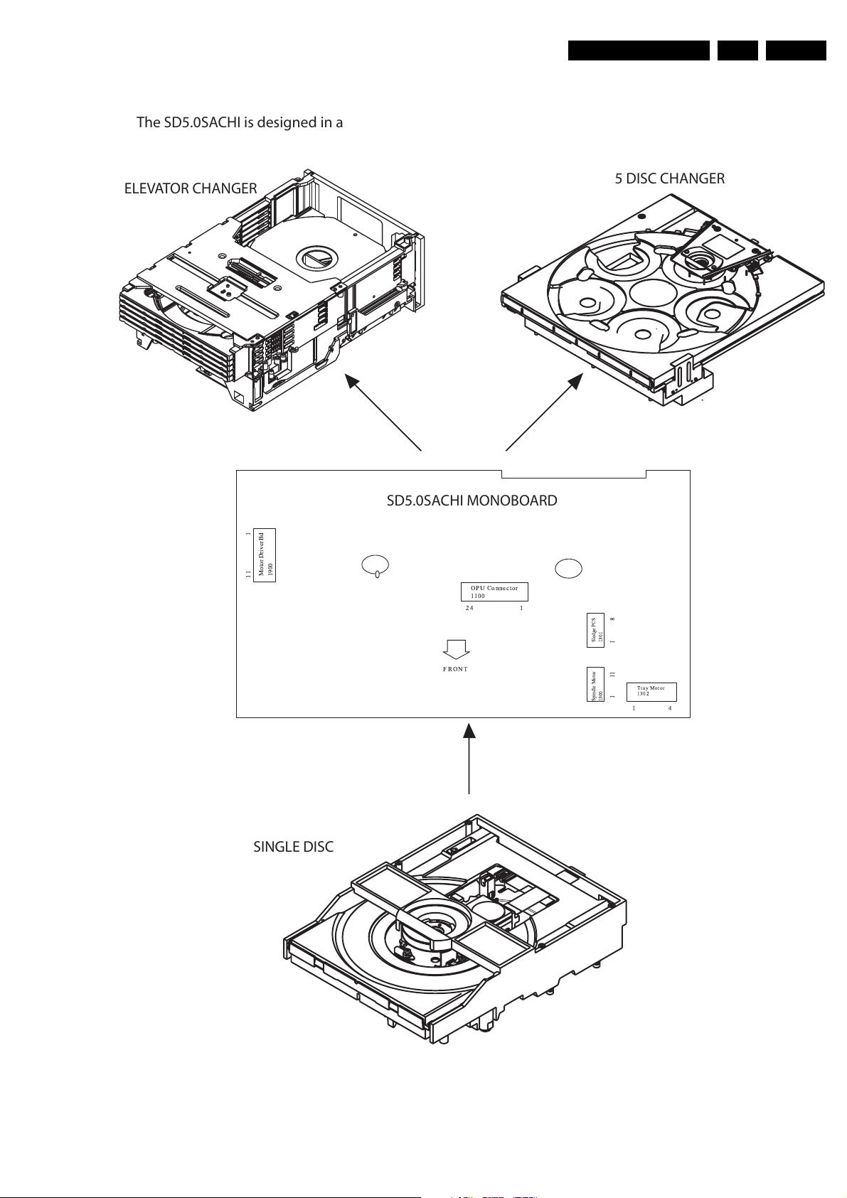
The SD5.0SACHI is designed in a multi-task way so that it can support the following
optional function.
EN 9SD-5.00SA_CH 4.
ELEVATOR CHANGER
5 DISC CHANGER
SD5.0SACHI MONOBOARD
!
SINGLE DISC
CL 36532056_015.eps
170703
Figure 4-2
EN 10 SD-5.00SA_CH4.
Mechanical Instructions
4.1.1 Dismantling of DVD Mono Board
1. See Figure 4-1 for dismantling of DVD module.
2. Unlock the OPU conn 1100, Sledge motor conn 1301
and disc motor conn 1300 and remove the Flex
connections.
3. Remove the wire connection to Tray motor conn 1302.
4. Remove 4 screws 10 to 13.
5. Remove the Mono Board
Note: Flex cables are very fragile,care should be taken during
dismounting and when mounting,ensure that Flex cables are
inserted properly into the Flex socket and locked.
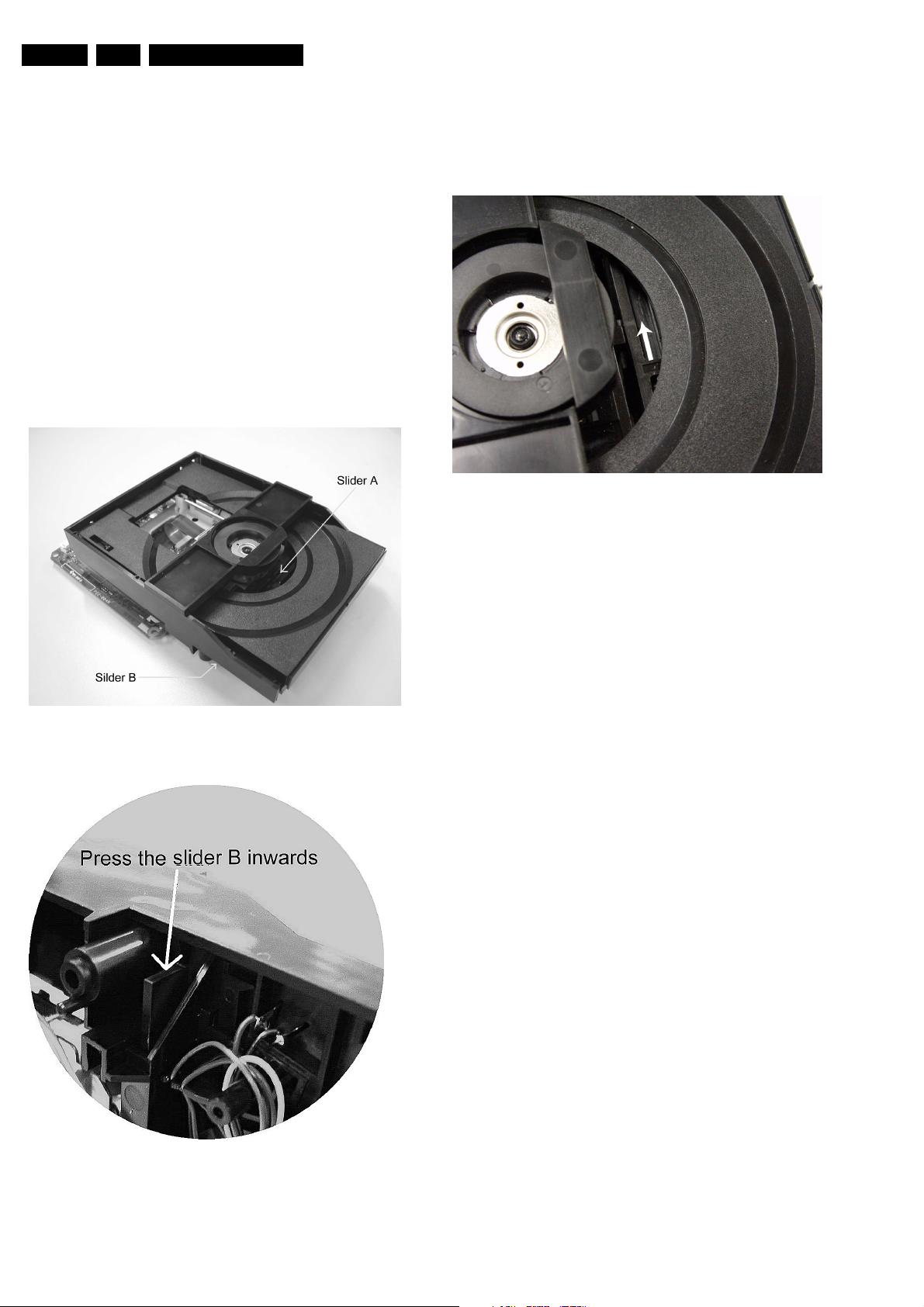
4.1.2 Opening of Tray Manually
Figure 4-3.The Tray is now disengaged and can be pulled
outwards.
When no disc is loaded, unlocking the Tray can also be done
by moving the Slider A in the direction as shown in Figure 4-4
and pull the Tray outwards.
CL 06532147_043.eps
231100
Figure 4-5
Figure 4-3
CL 06532147_002.eps
151100
Note: In this manual, only the dismantling instruction for
Single-disc loader is given.
Instruction for changer, refer to the respective player's service
manual.
CL 06532147_003.eps
151100
Figure 4-4
It is possible to open the tray manually by moving the Slider in
the position as shown in Figure 4-2 and Figure 4-3
When the slider A is not accessible when a disc is loaded,
unlock the tray by pressing the slider B inward as shown in
4.2 Service Hints
4.2.1 DVD Module
This module can be repaired as follows:
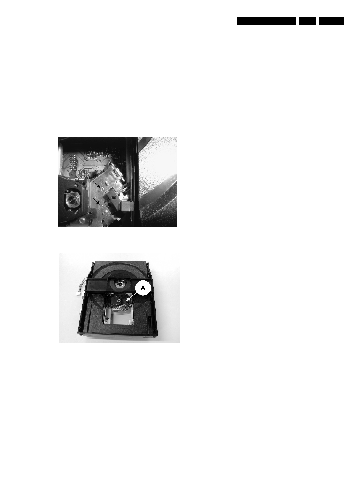
1. The VAL6011/14 is a combination of loading mechanism
and DVD-mechanism. Both the mechanism is not a
repairable unit and in case of failure it has to be replaced
with a new loader VAL6011/14.
Note: When replacing with a new VAL6011/14 two solder
joints have to be removed after connecting the OPU flex foil
to the board.
The solder joints which shortcircuits the laser diodes to
ground are for protection against ESD. Refer to Figure 4-5
and Figure 4-6 for location of solder points.
Mechanical Instructions
EN 11SD-5.00SA_CH 4.
Figure 4-6
Figure 4-7
2. The mono board has to be repaired down to component
level. Repair handling of the monoboard requires a
workshop with sophisticated desoldering tools.
EN 12 SD-5.00SA_CH5.
Test Instructions Mono Board DVD-SD5.00SA_CH
5. Test Instructions Mono Board DVD-SD5.00SA_CH
5.1 General
• Impedance of measuring-equipment should be > 1MΩ.
• Most tests have to be done by software commands.
Together with the software command you will find a Ref.#
nbr. This is the number of the diagnostic nulceus used for
this test. More detailed information can be find in the
chapter “Diagnostic Nuclei”.
• Levels: Most measurements are digital measurements.
The signal levels specification in this document are defined
as follows:
low:< 0.3V
high:> 3.0V
LOW:< 0.4V
HIGH:> 4.5V
• All the waveforms measurement carried out in these test
instruction will be base on the testpoint indicated in the
Monoboard schematic diagram in the service manual.
5.2 General Start-up Measurements
5.2.1 Supply Check:
Table 5-1 Supply check
Testpoint Supply Used by
F781 +3V3 Main supply voltage
F782 +5V Main supply voltage
F783 +12V Main supply voltage
F710 +3V3SA Analog 3V3 front-end circuitry
F711 +3V3SD Digital 3V3 front-end circuitry
F785 FUR-3V3 Digital 3V3 Furore2 interface
circuitry
F784 +3V3ST Digital 3V3 back-end circuitry
F724 3V3D Digital 3V3 cicuitry
F787 FUR-1V8 Digital 1V8 Furore2 core circuitry
F786 VDDA-FUR Analog 1V8 Furore2 circuitry
F717 +5VSA Analog 5V front-end circuitry
F715 +5VSD Digital 5V front-end circuitry
F721 +5VAV Analog 5V back-end circuitry
F718 +5VD Digital 5V back-end circuitry
F727 VDDSTA Analog STi 55xx circuitry
F729 VDDSTC Core STi 55xx circuitry
F725 VDDSTD Digital STi 55xx circuitry
STi 55xx uses various power supply voltages that depend on
which processor is being used
Table 5-2 Back-end processor
Back-end
Processor
STi 5580 +2V5 +2V5 +2V5
STi 5588 +1V8 +1V8 +3V3
STi 5519 +2V5 +2V5 +2V5
VDDSTA
( Analog )
VDDSTC
( Core )
VDDSTD
( Digital )
5.2.2 Reset Check:
To ensure a proper start-up of the monoboard, the back-end
reset signal RESETn is required at the STi55xx input (testpoint
F906) after power-on.
To check the reset timing, measure the RESETn (testpoint
F906) and the +3V3ST supply (testpoint F784), reset circuit
trigger signal.
PM3380B
ch1: dT=73.0ms V1= 65.0mV
ch1
ch2
T
1
2
CH1 2.00 V=
CH2 2.00 V= MTB50.0ms- 2.92dv ch1+
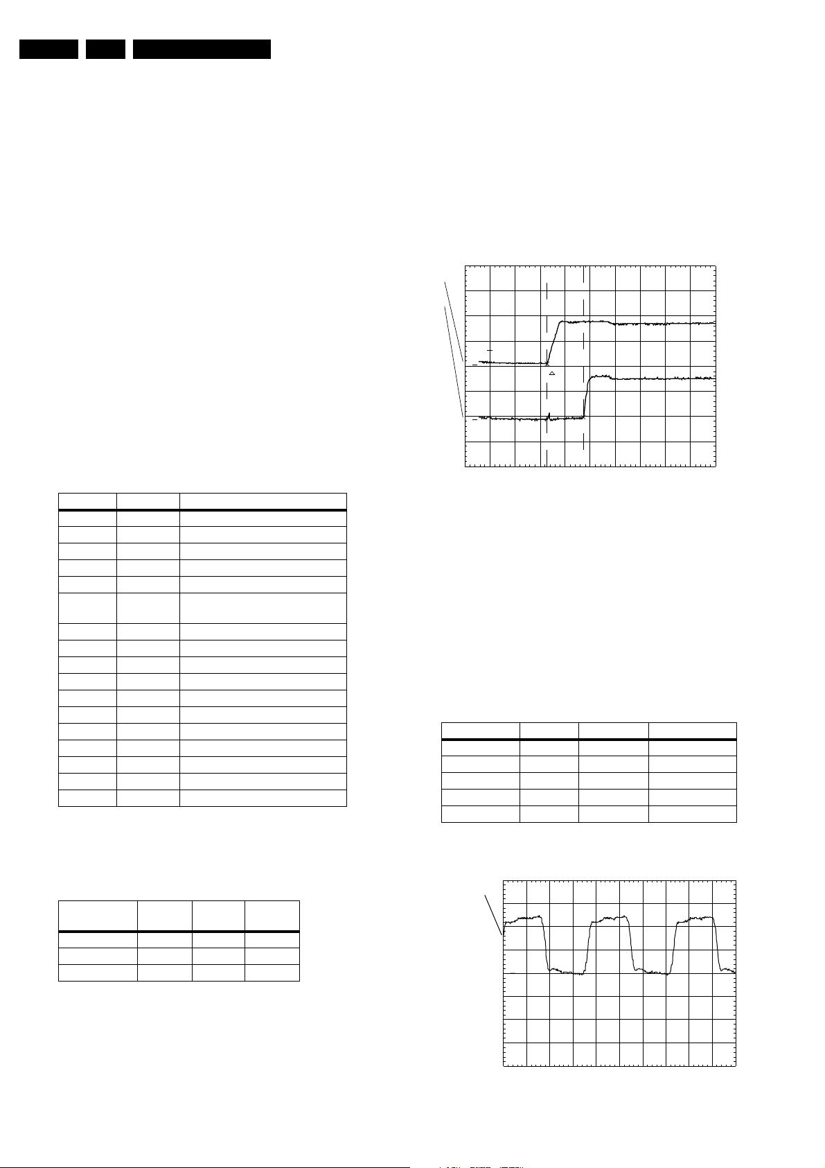
Figure 5-1 Reset
Nb: The RESETn rising edge should be at least 100msec after
the +3V3ST (refer to Figure 5-1).
If the reset input does not go high then check the reset circuit
around transistor 7409.
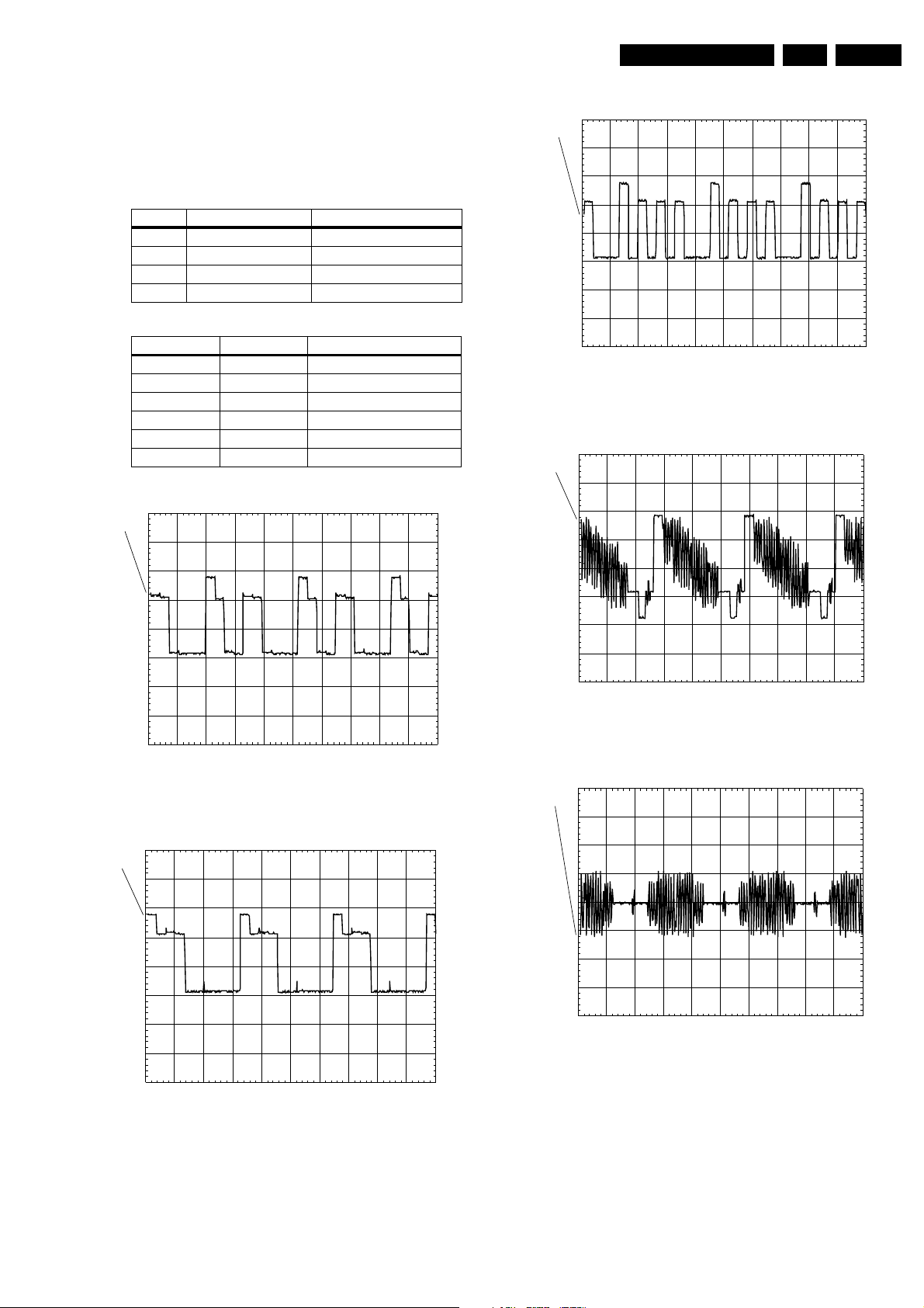
5.2.3 Clock Check
To check the correct functioning of the STI55xx, we first have
to check the presence of all clocks.
All clocks to be measured with 0.02% tolerance.
Table 5-3 Clock check
Name Testpoint Frequency Waveform
384FS F042 16.9344MHz Refer to Fig 5-3
27M_CLK_ST F932 27MHz Refer to Fig 5-2
PCM_CLK_ST F885 11.2896MHz Refer to Fig 5-5
Audio_CLK F935 11.2896MHz Refer to Fig 5-5
Iguana_CLK F207 8.4672MHz Refer to Fig 5-4
PM3380
B
ch1
CL 16532163_019.eps
290102
The module operates in power-off and power-on only. There is
no standby mode at module level. In power-off, the module
does not response to any communication or signals.
Before starting the measurement, ensure that all power supply
are connected to the monoboard via connector 1703 or 1701
and that the PC interface cable is connected to the Service
interface connector 1500 of the monoboard.
CH1 2.00 V= MTB10.0ns ch1+
CL 26532053_062.eps
Figure 5-2 27M_CLK
210502
Test Instructions Mono Board DVD-SD5.00SA_CH
PM3380
B
ch1
CH1 2.00 V= MTB20.0ns ch1+
Figure 5-3 384FS
PM3380B
ch1
CL 26532053_063.eps
210502
EN 13SD-5.00SA_CH 5.
Table 5-4 PC connection
Connector pin Signal
1500-1 TXT_SER (STi55xx out)
1500-2 SERVICE-mode select
1500-3 RXD_SER (STi55xx in)
1500-4 RTS_SER (Not in use)
1500-5 GND
1500-6 CTS_SER (Not in use)
1500-7 +5V_SER
Now start the terminal program. Make sure that the service-pin
(pin 1500-2) of the µP is pulled low.
The terminal program of your PC should now display: “DVDv4
Diagnostic software version ...”. This message already means
that the µP is running. The first 5 commands from the
diagnostic software will be carried out automatically during
diagnostic start-up. The other commands can be carried out by
selecting the “command input” and simply type the reference
nbr. to do the test or select the “Menu - driven” test.
To be sure that the µP is able to run the diagnostic software,
serial port will be checked during start-up.
Table 5-5 Serial port check
CH1 1.00 V= MTB50.0ns ch1+
Figure 5-4 Iguana_CLK
PM3380B
ch1
CH1 2.00 V= MTB20.0ns ch1+
CL 26532053_064.eps
CL 26532053_065.eps
210502
210502
Ref. # Reference Name Remark
(1) BasicSpAcc Serial port Access test/
initialisation
(2b) BasicInterconSdram Check SDRAM
interconnection with CPU
(4) BasicSdramWrR Check Basic SDRAM
memory
With this test, the serial communication is checked in both
directions.
Figure 5-5 PCM_ST_CLK / Audio_CLK
5.3 µP Environment:
5.3.1 General:
All the tests are carried out by software tests. To start the
software tests, connect a PC to the serial bus of the STI55xx.
Use connector 1500 for this connection:
EN 14 SD-5.00SA_CH5.
Test Instructions Mono Board DVD-SD5.00SA_CH
5.3.2 Memory Check:
The µP has a data bus that is connected to a Flash and also
internal link to the MPEG SDRAM inteface.
At start-up,the SDRAM bus is checked
Table 5-6 Memory check
Ref. # Command Name Remark
(2b) BasicInterconSDRAM Data and address bus
Interconnection
6 PapChksFl Checksum FLASH
16 CompSdramWrR SDRAM Write Read
CompSdramWrR checks the complete SDRAM for failures
inside the IC.The BasicInterconSDRAM check is done by
writing & reading some well chosen patterns to all address and
data interconnections of the SDRAM.
The PapChksFI calculate and verify checksum of the FLASH.
This includes the binary file checksum and the four modules.
5.4 General I/O Port & Peripherals Check
5.4.1 I2C Bus / EEprom Check
To access the EEprom, the I2C bus is used. So by writing and
reading to the EEprom the chip and the bus is checked. With
next commands a certain byte is written to the EEprom. The
original information will always be written back into the
EEprom.
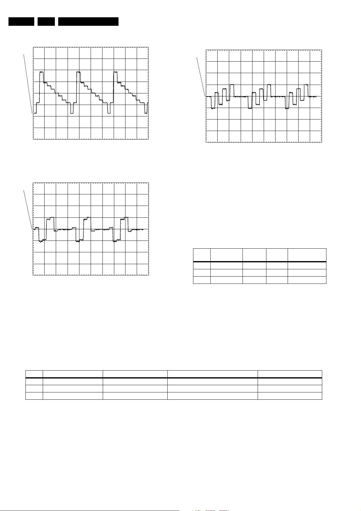
5.4.2 Audio Clock Switch Check
The internally generated Audio clock can be set to either 44.1
kHz (CD_DA), 48 kHz (DVD) or 96 kHZ (DVD). To check the
different mode, use the following commands and measure the
waveform as correct operation cannot be detected by the
Diagnostic Software.
Table 5-9 Audio clock switch check
Command
Ref #
Name Remark
7a PapUclkAclk
Cdda
µClock A_CLK
in 44.1kHz
Test
point Frequency
T885 11.2896MHz
mode( Fig 5-4 )
7b PapUclkAclk
Dvd
µClockA_CLK
in 48kHz mode
T885 12.288MHz
( Fig 5-5 )
7c PapUclkAclk
Dvd96
µClock A_CLK
in 96kHz mode
T885 24.576MHz
( Fig 5-6 )
PM3380B
ch1
0.02%
0.02%
0.02%
Table 5-7 EEprom check
Ref. # Command Name Remark
11 PapI2cNvram I2C NVRAM access
The complete Eeprom can also be checked on failures by
writing to all addresses and reading back. This test takes a long
time (110 sec).
Table 5-8
Ref. # Command Name Remark
15 PapNvramWrR NVRAM Write Read
CH1 2.00 V= MTB20.0ns ch1+
CL 26532053_066.eps
Figure 5-6 µClock A_CLK in 44.1kHz mode
PM3380B
ch1
1
CH1 2.00 V= MTB20.0ns ch1+
CL 26532053_067.eps
210502
210502
Figure 5-7 µClockA_CLK in 48kHz mode
Test Instructions Mono Board DVD-SD5.00SA_CH
EN 15SD-5.00SA_CH 5.
PM3380B
ch1
1
CH1 2.00 V= MTB20.0ns ch1+
Figure 5-8 µClock A_CLK in 96kHz mode
5.4.3 Audio Mute Check
Switch on the Mute circuit by sending next command:
Table 5-10 Audio mute check
Ref. # Command Name Remark
19a AudioMuteOn AudioMuteOn
CL 26532053_068.eps
210502
Table 5-13 NameTestpointWaveform
Name Testpoint Waveform
PCMLRCLK F886 / F021 Refer to Figure 5-9
PCMSCLK F883 / F019 Refer to Figure 5-
10
PCMDATA0 F884 Refer to Figure 5-
11
DATA_LR/DSD_LEFT F025 Refer to Figure 5-
11
DATA_LsRs/DSD_Ls F029 Refer to Figure 5-
11
DATA_CL/
DSD_CENTRE
F034 Refer to Figure 5-
11
PCMCLK F885 / F016 Refer to Figure 5-
12
SPDIF F719 Refer to Figure 5-
13
PM3394B
ch1
Check the Mute output again at testpoint T798: 3V3 ±10%
Switch off the Mute circuit by sending next command
Table 5-11 Audio mute check
Ref. # Command Name Remark
19a AudioMuteOff AudioMuteOff
Check the Mute output at testpoint T798: 0V ±0.3V
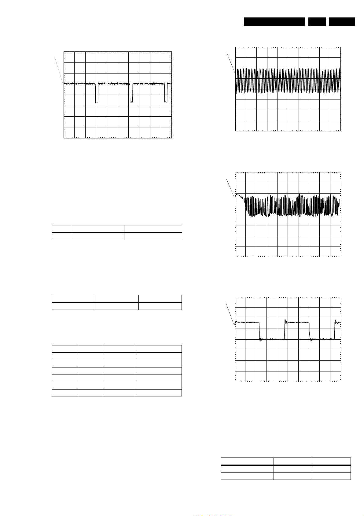
5.4.4 Audio I2S Check
To check the audio output, connect a audio DAC (on the A/V
board) to the I2S output and start-up the audio test. Look at the
audio outputs from the A/V board for both sine and pink noise.
Table 5-12 Audio I2S check
Command
Ref. #
21a AudioSineOn Audio Sine
Name Remark Audio outputs
Audio Sine signal On
signal Off
Sine, 1kHz on stereo
Press stop button
20a AudioPinkNoi
seOn
Audio
Pinknoise
Pink Noise on 6
channels
On
20b AudioPinkNoi
seOff
Audio
Pinknoise
Off
1
CH1 2.00 V~ MTB10.0us ch1+
Figure 5-9 PCMLRCLK
PM3394B
ch1
1
CH1 2.00 V~ MTB 100ns ch1+
Figure 5-10 PCMSCLK
CL06532065_008.eps
CL06532065_009.eps
161100
161100
The audio signal (sine or pink noise) will also be present on the
digital ouput (SPDif). This can be checked by connecting an
amplifier with digital input.
Check the I2S output.
EN 16 SD-5.00SA_CH5.
PM3394B
ch1
Test Instructions Mono Board DVD-SD5.00SA_CH
Alternatively, there is a check that can be done without A/V
board.
First, let the decoder generate pink noise on the audio outputs.
Table 5-14
Ref. # Command Name Remark
20a AudioPinkNoiseOn Audio Pinknoise On
1
CH1 1.00 V~ MTB 500ns ch1+
Figure 5-11 PCMDATA
PM3380B
ch1
1
CH1 2.00 V= MTB20.0ns ch1+
CL06532065_010.eps
161100
CL 26532053_067.eps
Measure then these signals on level and frequency.
Table 5-15
Signal Level between Frequency
PCMLRCLK low/high 48kHz 0.02%
PCMSCLK low/high 3.072MHz 0.02%
PCMCLK low/high 12.288MHz 0.02%
PCMDATA low/high N/A
SPDIF LOW/HIGH N/A
Put the pink noise off:
Table 5-16
Ref. # Command Name Remark
20b AudioPinkNoiseOff Audio Pinknoise Off
210502
Figure 5-12 PCMCLK
PM3380B
ch1
1
CH1 2.00 V= BWL MTB100ns ch1+
CL 16532163_024.eps
230102
Figure 5-13 SPDIF
To switch the audio signal OFF, press the STOP button on the
front.
Without A/V board, the switching levels are as follows:
– DATA_LsRs and DATA_CL switch between low and high
for pink noise. For sine, this is low.
– PCMDATA0, PCMLRCLK, PCMCLK and PCMSCLK
switches between low and high for both pink noise and
sine.
– SPDIF switches between LOW and HIGH
Test Instructions Mono Board DVD-SD5.00SA_CH
EN 17SD-5.00SA_CH 5.
5.5 VIDEO
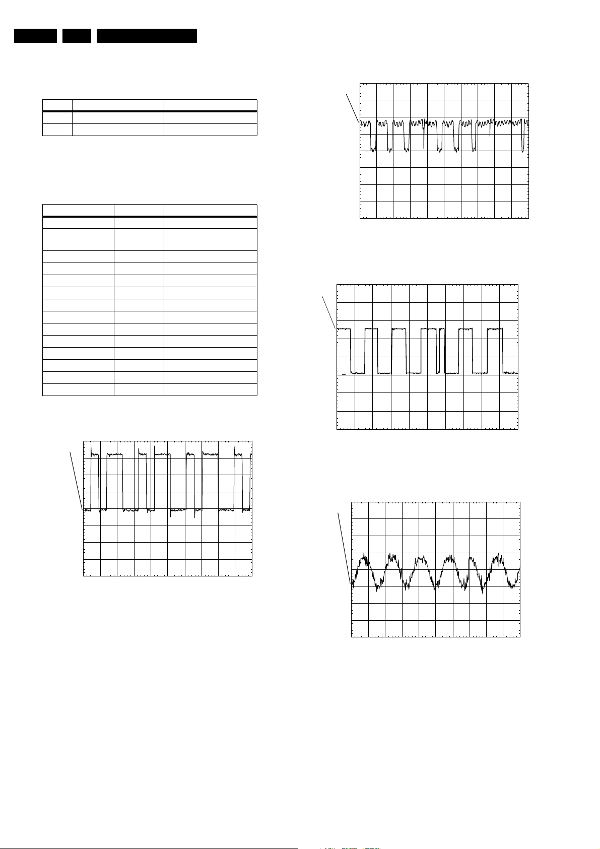
5.5.1 Video Output Check
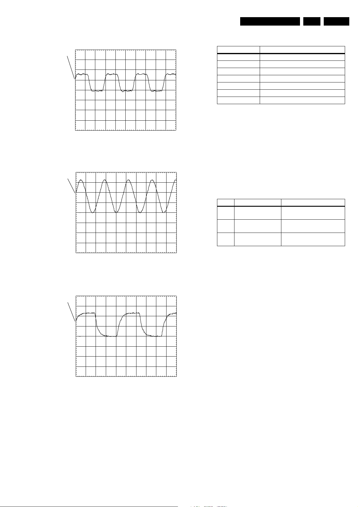
Measure the DC voltages at all video-outputs at conn 1703
while the video signal is turned off: 1V ± 10%
Generate a color-bar via next software commands:
Ref. # Command Name Remark
23a VideoColDencOn Colourbar DENC ON
61a VideoColOutRGB RGB Colourbar
61b VideoColOutYUV YUV Colourbar
23b VideoColDencOff Colourbar DENC OFF
Check video output at the next testpoints:
Name Testpoint Waveform
R_VID (V) F795 Refer to Figure 5-14 5-20
G_VID (Y) F796 Refer to Figure 5-15
B_VID (U) F799 Refer to Figure 5-16 5-21
CVBS_VID F788 Refer to Figure 5-17
C_VID F791 Refer to Figure 5-18
Y_VID F792/F796 Refer to Figure 5-19
PM3380B
ch1
PM3380B
ch1
1
RUN
CH1 5 00mV~ BWLMTB20.0u s ch1+
Figure 5-16 B_VID (U) with video out at RGB
PM3380B
ch1
CL 16532163_058.eps
290102
1
CH1 500mV~ BWLMTB20.0us ch1+
Figure 5-14 R_VID (V) with video out at RGB
PM3380B
ch1
1
CL 16532163_056.eps
290102
1
RUN
CH1 500mV~ BWL MTB20.0us ch1+
Figure 5-17 CVBS_VID
PM3380B
ch1
1
CH1 500mV~ BWL MTB20.0us L=1 ch1p
CL 16532163_059.eps
290102
CL 16532163_060.eps
290102
CH1 500mV~ BWLMTB20.0us ch1+
CL 16532163_057.eps
Figure 5-15 G_VID (Y) with video out at RGB
Figure 5-18 C_VID
290102
EN 18 SD-5.00SA_CH5.
Test Instructions Mono Board DVD-SD5.00SA_CH
PM3380B
ch1
1
CH1 500mV~ BWLMTB20.0us L=1 ch1p
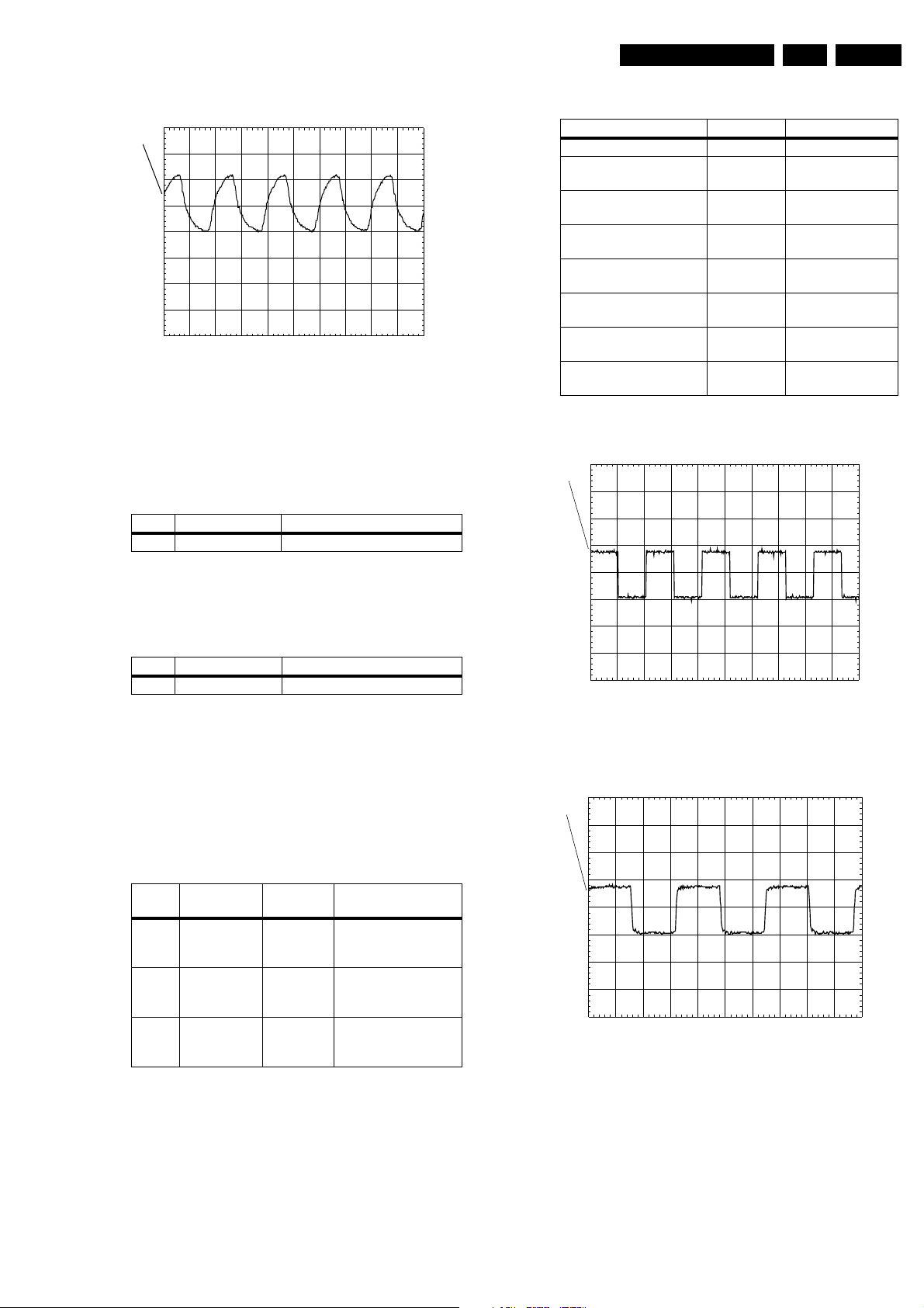
Figure 5-19 Y_VID
PM3380B
ch1
1
CL 16532163_061.eps
290102
PM3380B
ch1
1
CH1 500mV~ BWLMTB20.0us L=1 extp
Figure 5-21 B_VID (U) with video out at YUV
5.5.2 Slow Blanking Scart
An aditional part of the video-path is the scart functionswitching test. The scart function-switching pin has three levels
which depend on the level of the output ports SCART0 and
SCART1. These latter two signals are driven by the output pins
PIO3.6 and PIO3.7 of the STi55xx.
Check the level of SCART0 and SCART1 with the following
commands:
Table 5-17 Slow blanking scart
CL 16532163_026.eps
230102
CH1 500mV~ BWLMTB20.0us L=1 ext p
Figure 5-20 R_VID (V) with video out at YUV
5.5.3 Video Hsync Check.
To measure the Video Hsync, the connector 1704 must be
connected to the external video processing device such as high
quality progressive scan codex and high quality Video DAC,
else there will not be any waveform. To check for the Hsync,
the following commands can be used:
Table 5-18 Video Hsync check
Ref. # Command Name Remark Value Waveform
23a VideoColDencOn ColourbarDENC ON 15.625 kHz 0.02% Vpeak-peak > 3V Refer to Fig 5-22
61a VideoColOutRGB RGB Colourbar ON 15.625 kHz 0.02% Vpeak-peak > 3V Refer to Fig 5-22
23b VideoColDencOff Colourbar DENC OFF No measurements needed
CL 16532163_025.eps
230102
Ref. #
Command
Name
Scart0
(PIO3.6)
Scart1
(PIO3.7)
Level on Pin 8
of scart
25a VideoScartLo 1 1 0-2V
25b VideoScartMi 0 1 4.5-7V
25c VideoScartHi 0 0 9.5-12V
Test Instructions Mono Board DVD-SD5.00SA_CH
EN 19SD-5.00SA_CH 5.
PM3394B
ch1
1
CH1 2.00 V~ MTB20.0us ch1+
HSYNC
Figure 5-22 Video H Sync
5.6 Servo
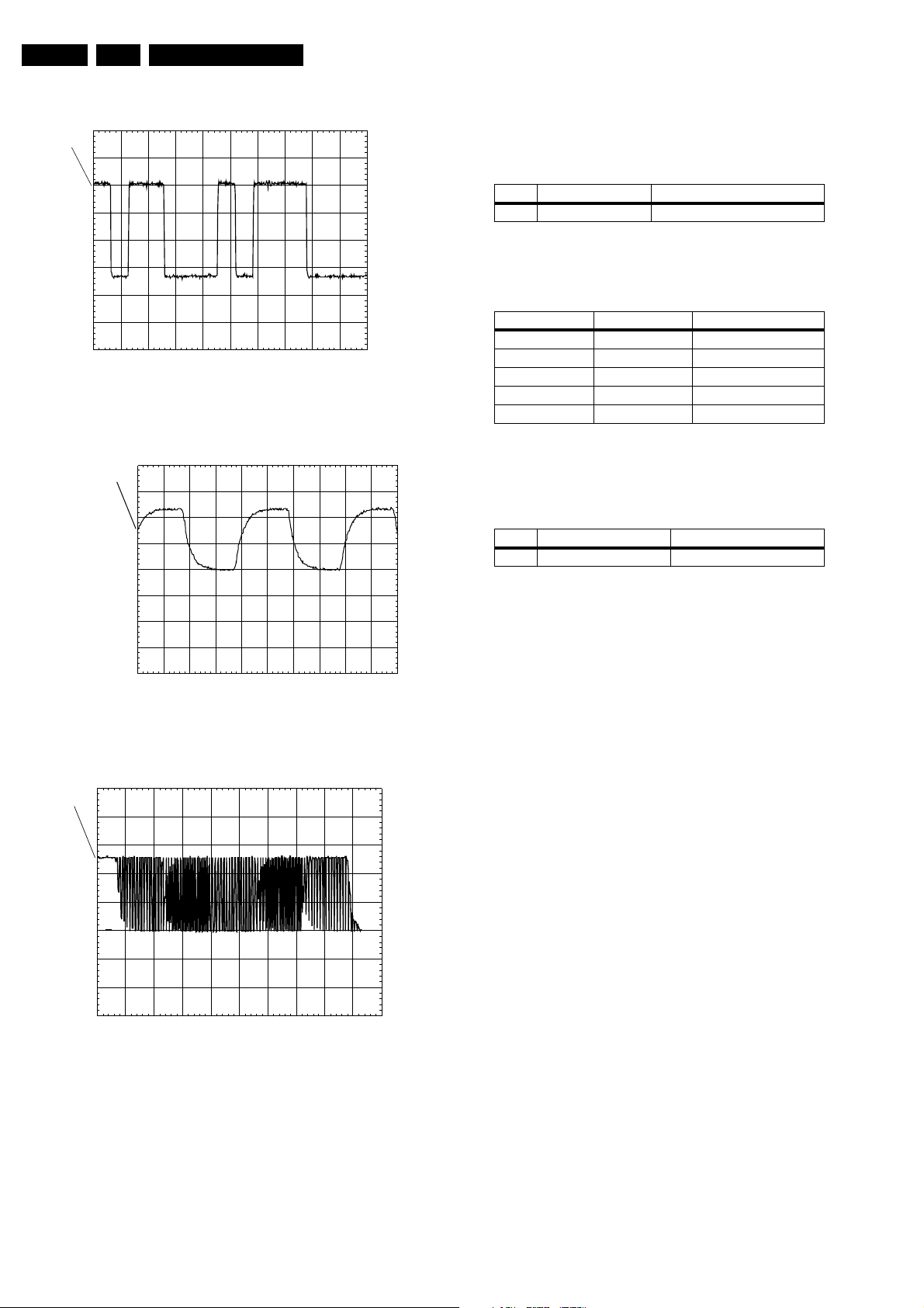
5.6.1 General Start-up Measurements:
Reset the Basic Engine part
Table 5-19 Reset basic engine part
CL06532065_019.eps
161100
PM3380B
ch1
1
CH1 2.00 V= MTB 200ns ch1+
Figure 5-23 BE_BCLK
PM3380B
ch1
1
CL 16532163_027.eps
230102
Ref. # Command Name Remark
44 BeReset Reset the Basic Engine
Check if the Servo Reset (RSTN) at testpoint F258 goes from
low to high after executing BeReset commands.
Check Vref
Table 5-20 Vref check
Name Testpoint Value
Vref F111 2.5V 0.3V
Play DVD test Disc and check I2S interface
Table 5-21 I2S interface check
Name Testpoint Value Value
BE_BCLK F200 6.0 MHz ± 0.1 Refer to Figure 5-23
BE_WCLK F201 high Refer to Figure 5-25
BE_DATA F202 low Refer to Figure 5-24
BE_FLAG F203 low No waveform
BE_V4 F255 low No waveform
BE_SYNC F256 low No waveform
CH1 2.00 V= MTB20.0ns ch1+
Figure 5-24 BE_DATA
PM3380B
ch1
1
CH 1 2.00 V= MTB 200ns c h1 +
Figure 5-25 BE_WCLK
CL 16532163_028.eps
230102
CL 16532163_029.eps
230102
5.6.2 Spindle Motor:
Before switching on the discmotor, check the following
testpoints:
Table 5-22 Spindle motor check
Name Testpoint Value
STDBY_MOTOR F308 low
MOTO1 F350 1V5 0.3
EN 20 SD-5.00SA_CH5.
Switch the Discmotor ON/OFF with the following commands:
Table 5-23 Disc motor switching
Ref. # Command Name Remark
39a BeDiscmotorOn Discmotor on
39b BeDiscmotorOff Discmotor off
Check the following signals with the discmotor switched ON
and without DVD Disc inserted.
Table 5-24 Disc motor switching
Test Instructions Mono Board DVD-SD5.00SA_CH
PM3380B
ch1
Name Testpoint Frequency
STDBY_MOTOR F308 high
MOTO1 I241 4Vpp ± 0.5V Refer to
Figure 5-26
A3 F301 Refer to Figure 5-27
A2 F302 Refer to Figure 5-27
A1 F303 Refer to Figure 5-27
T1 F210 Refer to Figure 5-28
T2 F211 Refer to Figure 5-28
T3 F212 Refer to Figure 5-28
H1+ F306 Refer to Figure 5-29
H1- F304 Refer to Figure 5-29
H2+ F309 Refer to Figure 5-29
H2- F305 Refer to Figure 5-29
H3+ F311 Refer to Figure 5-29
H3- F313 Refer to Figure 5-29
PM3380B
ch1
CH1 5.00 V= MTB50.0ms ch1
Figure 5-27 A1-A2-A3
PM3380B
ch1
1
CH1 2.00 V= MTB5.00ms ch1+
Figure 5-28 T1-T2-T3
PM3380B
CL 26532053_070.eps
CL 16532163_032.eps
210502
230102
CH1 1.00 V= MTB 250ns ch1
CL 26532053_069.eps
Figure 5-26 Motor 1
210502
ch1
CH1 200mV~ MTB5.00ms ch1
CL 26532053_071.eps
Figure 5-29 H1+ ; H1- ; H2+ ; H2- ; H3+ ; H3-
When measurement is completed, switch the discmotor OFF
before executing next command
5.6.3 Radial
Radial ON will only work when the PCB is connected to a CDM
and DVD Disc is inserted.
Switch the Radial control ON/OFF with the following
commands:
210502
 Loading...