

Philips SCN2681TC1A44 Datasheet

INTEGRATED CIRCUITS
SCN2681T
Dual asynchronous receiver/transmitter
(DUART)
Product specification
Supersedes data of 1995 May 01
IC19 Data Handbook
1998 Sep 04

Philips Semiconductors Product specification
SCN2681TDual asynchronous receiver/transmitter (DUART)
DESCRIPTION
The Philips Semiconductors SCN2681 Dual Universal
Asynchronous Receiver/Transmitter (DUART) is a single-chip
MOS-LSI communications device that provides two independent
full-duplex asynchronous receiver/transmitter channels in a single
package. The SCN2681T features a faster bus cycle time than the
standard SCN2681. The quick bus cycle eliminates or reduces the
need for wait states with fast CPUs and permits high throughput in
I/O intensive systems. Higher external clock rates may be used with
the transmitter, receiver and counter timer which in turn provide
greater versatility in baud rate generation. The SCN2681T
interfaces directly with microprocessors and may be used in a polled
or interrupt driven system.
The operating mode and data format of each channel can be
programmed independently. Additionally, each receiver and
transmitter can select its operating speed as one of eighteen fixed
baud rates, a 16X clock derived from a programmable counter/timer,
or an external 1X or 16X clock. The baud rate generator and
counter/timer can operate directly from a crystal or from external
clock inputs. The ability to independently program the operating
speed of the receiver and transmitter make the DUART particularly
attractive for dual-speed channel applications such as clustered
terminal systems.
Each receiver is quadruple buffered to minimize the potential of
receiver over-run or to reduce interrupt overhead in interrupt driven
systems. In addition, a flow control capability is provided to disable
a remote DUART transmitter when the receiver buffer is full.
Also provided on the SCN2681T are a multipurpose 7-bit input port
and a multipurpose 8-bit output port. These can be used as general
purpose I/O ports or can be assigned specific functions (such as
clock inputs or status/interrupt outputs) under program control.
For a complete functional description and programming information
for the SCN2681T, refer to the SCN2681 product specification.
FEA TURES
•Fast bus cycle times reduce or eliminate CPU wait states
•Dual full-duplex asynchronous receiver/transmitters
•Quadruple buffered receiver data registers
•Programmable data format
– 5 to 8 data bits plus parity
– Odd, even, no parity or force parity
– 1, 1.5 or 2 stop bits programmable in 1/16-bit increments
•16-bit programmable Counter/Timer
•Programmable baud rate for each receiver and transmitter
selectable from:
– 22 fixed rates: 50 to 115.2k baud
– Non-standard rates to 115.2
– Non-standard user-defined rate derived from programmable
counter/timer
– External 1X or 16X clock
•Parity, framing, and overrun error detection
•False start bit detection
•Line break detection and generation
•Programmable channel mode
– Normal (full-duplex)
– Automatic echo
– Local loopback
– Remote loopback
•Multi-function programmable 16-bit counter/timer
•Multi-function 7-bit input port
– Can serve as clock or control inputs
– Change of state detection on four inputs
– 100kΩ typical pull-up resistors
•Multi-function 8-bit output port
– Individual bit set/reset capability
– Outputs can be programmed to be status/interrupt signals
•Versatile interrupt system
– Single interrupt output with eight maskable interrupting
conditions
– Output port can be configured to provide a total of up to six
separate wire-ORable interrupt outputs
•Maximum data transfer rates:
1X – 1MB/sec transmitter and receiver; 16X – 500kB/sec receiver
and 250kB/sec transmitter
•Automatic wake-up mode for multidrop applications
•Start-end break interrupt/status
•Detects break which originates in the middle of a character
•On-chip crystal oscillator
•Single +5V power supply
•Commercial and industrial temperature ranges available
ORDERING INFORMATION
DESCRIPTION VCC = +5V +10%, TA = 0°C to +70°C DWG #
40-Pin Plastic Dual In-Line Package (600mil-wide DIP) SCN2681TC1N40 SOT129-1
44-Pin Plastic Lead Chip Carrier (PLCC) SCN2681TC1A44 SOT187-2
NOTE: For a full register description and programming information see the SCN2681.
1998 Sep 04 853–1002 19970
2
Philips Semiconductors Product specification
SCN2681TDual asynchronous receiver/transmitter (DUART)
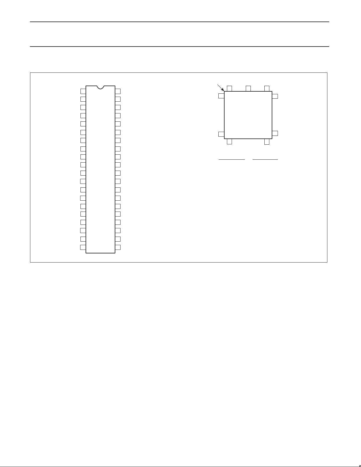
PIN CONFIGURATIONS
INDEX
A0
IP3
A1
IP1
A2
A3
IP0
WRN
RDN
RxDB
TxDB
OP1
OP3
OP5
OP7
D1
D3
D5
D7
GND
1
2
3
4
5
6
7
8
9
10
DIP
11
12
13
14
15
16
17
18
19
40
39
38
37
36
35
34
33
32
31
30
29
28
27
26
25
24
23
22
2120
NOTE:
Refer to SCN2681 for functional description.
V
CC
IP4
IP5
IP6
IP2
CEN
RESET
X2
X1/CLK
RxDA
TxDA
OP0
OP2
OP4
OP6
D0
D2
D4
D6
INTRN
CORNER
Figure 1. Pin Configurations
6
7
17
18
PIN/FUNCTION PIN/FUNCTION
1NC 23NC
2 A0 24 INTRN
3 IP3 25 D6
4A1 26D4
5 IP1 27 D2
6A2 28D0
7 A3 29 OP6
8 IP0 30 OP4
9 WRN 31 OP2
10 RDN 32 OP0
11 RxDB 33 TxDA
12 NC 34 NC
13 TxDB 35 RxDA
14 OP1 36 X1/CLK
15 OP3 37 X2
16 OP5 38 RESET
17 OP7 39 CEN
18 D1 40 IP2
19 D3 41 IP6
20 D5 42 IP5
21 D7 43 IP4
22 GND 44 V
1
PLCC
TOP VIEW
40
28
CC
SD00098
39
29
1998 Sep 04
3
Philips Semiconductors Product specification
SCN2681TDual asynchronous receiver/transmitter (DUART)
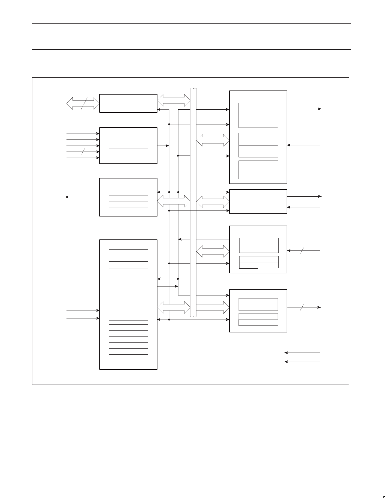
BLOCK DIAGRAM
D0–D7
RDN
WRN
CEN
A0–A3
RESET
INTRN
8
BUS BUFFER
OPERATION CONTROL
ADDRESS
4
DECODE
R/W CONTROL
INTERRUPT CONTROL
IMR
ISR
TIMING
BAUD RATE
GENERATOR
CLOCK
SELECTORS
CONTROL
TIMING
INTERNAL DATABUS
CHANNEL A
TRANSMIT
HOLDING REG
TRANSMIT
SHIFT REGISTER
RECEIVE
HOLDING REG (3)
RECEIVE
SHIFT REGISTER
MRA1, 2
CRA
SRA
CHANNEL B
(AS ABOVE)
INPUT PORT
CHANGE OF
STATE
DETECTORS (4)
IPCR
ACR
TxDA
RxDA
TxDB
RxDB
7
IP0-IP6
X1/CLK
COUNTER/
TIMER
X2
XTAL OSC
CSRA
CSRB
ACR
U
CTLR
CTLR
OUTPUT PORT
FUNCTION
SELECT LOGIC
OPCR
OPR
8
OP0-OP7
V
CC
GND
SD00099
Figure 2. Block Diagram
1998 Sep 04
4

Philips Semiconductors Product specification
SCN2681TDual asynchronous receiver/transmitter (DUART)
PIN DESCRIPTION
MNEMONIC TYPE NAME AND FUNCTION
D0–D7 I/O Data Bus: Bidirectional three-state data bus used to transfer commands, data and status between the DUART and
CEN I Chip Enable: Active low input signal. When low, data transfers between the CPU and the DUART are enabled on
WRN I Write Strobe: When low and CEN is also low, the contents of the data bus is loaded into the addressed register. The
RDN I Read Strobe: When low and CEN is also low , causes the contents of the addressed register to be presented on the
A0–A3 I Address Inputs: Select the DUART internal registers and ports for read/write operations.
RESET I Reset: A high level clears internal registers (SRA, SRB, IMR, ISR, OPR, OPCR), puts OP0–OP7 in the high state,
INTRN O Interrupt Request: Active-low, open-drain output which signals the CPU that one or more of the eight maskable
X1/CLK I Crystal 1: Crystal connection or an external clock input. A crystal of a clock the appropriate frequency (nominally
X2 I Crystal 2: Crystal connection. See Figure 7. If a crystal is not used it is best to keep this pin not connected although it
RxDA I Channel A Receiver Serial Data Input: The least significant bit is received first. ‘Mark’ is high, ‘space’ is low.
RxDB I Channel B Receiver Serial Data Input: The least significant bit is received first. ‘Mark’ is high, ‘space’ is low.
TxDA O Channel A Transmitter Serial Data Output: The least significant bit is transmitted first. This output is held in the ‘mark’
TxDB O Channel B Transmitter Serial Data Output: The least significant bit is transmitted first. This output is held in the
OP0 O Output 0: General purpose output, or channel A request to send (RTSAN, active-low). Can be deactivated
OP1 O Output 1: General purpose output, or channel B request to send (RTSBN, active-low). Can be deactivated
OP2 O Output 2: General purpose output, or channel A transmitter 1X or 16X clock output, or channel A receiver 1X clock output.
OP3 O Output 3: General purpose output, or open-drain, active-low counter/timer output, or channel B transmitter 1X clock
OP4 O Output 4: General purpose output, or channel A open-drain, active-low, RxRDYA/FFULLA output.
OP5 O Output 5: General purpose output, or channel B open-drain, active-low, RxRDYB/FFULLB output.
OP6 O Output 6: General purpose output, or channel A open-drain, active-low, TxRDYA output.
OP7 O Output 7: General purpose output, or channel B open-drain, active-low TxRDYB output.
IP0 I Input 0: General purpose input, or channel A clear to send active-low input (CTSAN). Pin has an internal VCC pull-up
IP1 I Input 1: General purpose input, or channel B clear to send active-low input (CTSBN). Pin has an internal VCC pull-up
IP2 I Input 2: General purpose input, or counter/timer external clock input. Pin has an internal VCC pull-up device supplying
IP3 I Input 3: General purpose input, or channel A transmitter external clock input (TxCA). When the external clock is used
IP4 I Input 4: General purpose input, or channel A receiver external clock input (RxCA). When the external clock is used by
IP5 I Input 5: General purpose input, or channel B transmitter external clock input (TxCB). When the external clock is used
IP6 I Input 6: General purpose input, or channel B receiver external clock input (RxCB). When the external clock is used by
V
CC
GND I Ground
the CPU. D0 is the least significant bit.
D0–D7 as controlled by the WRN, RDN, and A0–A3 inputs. When CEN is high, the DUART places the D0–D7 lines in
the three-state condition.
transfer occurs on the rising edge of the signal.
data bus. The read cycle begins on the falling edge of RDN.
stops the counter/timer, and puts channels A and B in the inactive state, with the TxDA and TxDB outputs in the mark
(high) state. Clears Test modes, sets MR pointer to MR1.
interrupting conditions are true.
3.6864 MHz) must be supplied at all times. For crystal connections see Figure 7, Clock Timing.
is permissible to ground it.
condition when the transmitter is disabled, idle, or when operating in local loopback mode. ‘Mark’ is high, ‘space’ is low.
‘mark’ condition when the transmitter is disabled, idle, or when operating in local loopback mode. ‘Mark’ is high,
‘space’ is low.
automatically on receive or transmit.
automatically on receive or transmit.
output, or channel B receiver 1X clock output.
device supplying 1 to 4 A of current.
device supplying 1 to 4 A of current.
1 to 4 A of current.
by the transmitter, the transmitted data is clocked on the falling edge of the clock. Pin has an internal VCC pull-up
device supplying 1 to 4 A of current.
the receiver, the received data is sampled on the rising edge of the clock. Pin has an internal VCC pull-up device
supplying 1 to 4 A of current.
I Power Supply: +5V supply input.
1998 Sep 04
5
 Loading...