

Philips SC4000 Datasheet

INTEGRATED CURCUITS
DATA SH EET
SC4000
Universal Timeslot Interchange
Preliminary specification
File under Integrated Curcuits
2000 Sep 07

Philips Semiconductors Preliminary specification
Universal Timeslot Interchange SC4000
Features . . . . . . . . . . . . . . . . . . . . . . . . . . . . . . . . . . . . . . . . . . . . . . . . . . . . . . . . . . . . . . . . . . . . . . . . . . . . . . . . . . . . . . . . . . . . . . . . . . . . . . . . . . .1
Applications . . . . . . . . . . . . . . . . . . . . . . . . . . . . . . . . . . . . . . . . . . . . . . . . . . . . . . . . . . . . . . . . . . . . . . . . . . . . . . . . . . . . . . . . . . . . . . . . . . . . . . .1
Logic Pin Organization . . . . . . . . . . . . . . . . . . . . . . . . . . . . . . . . . . . . . . . . . . . . . . . . . . . . . . . . . . . . . . . . . . . . . . . . . . . . . . . . . . . . . . . . . . . . . . . .1
Block Diagram . . . . . . . . . . . . . . . . . . . . . . . . . . . . . . . . . . . . . . . . . . . . . . . . . . . . . . . . . . . . . . . . . . . . . . . . . . . . . . . . . . . . . . . . . . . . . . . . . . . . . .2
SC4000 100-Pin TQFP (top view) . . . . . . . . . . . . . . . . . . . . . . . . . . . . . . . . . . . . . . . . . . . . . . . . . . . . . . . . . . . . . . . . . . . . . . . . . . . . . . . . . . . . . . .2
SC4000 Physical Dimensions (all dimensions in millimeters) . . . . . . . . . . . . . . . . . . . . . . . . . . . . . . . . . . . . . . . . . . . . . . . . . . . . . . . . . . . . . . . . . .3
Pin Description . . . . . . . . . . . . . . . . . . . . . . . . . . . . . . . . . . . . . . . . . . . . . . . . . . . . . . . . . . . . . . . . . . . . . . . . . . . . . . . . . . . . . . . . . . . . . . . . . . . .4
Device Overview . . . . . . . . . . . . . . . . . . . . . . . . . . . . . . . . . . . . . . . . . . . . . . . . . . . . . . . . . . . . . . . . . . . . . . . . . . . . . . . . . . . . . . . . . . . . . . . . . . .6
Function Description . . . . . . . . . . . . . . . . . . . . . . . . . . . . . . . . . . . . . . . . . . . . . . . . . . . . . . . . . . . . . . . . . . . . . . . . . . . . . . . . . . . . . . . . . . . . . . .8
Switching . . . . . . . . . . . . . . . . . . . . . . . . . . . . . . . . . . . . . . . . . . . . . . . . . . . . . . . . . . . . . . . . . . . . . . . . . . . . . . . . . . . . . . . . . . . . . . . . . . . . . . . . . .8
PLL Timing and Clock Control . . . . . . . . . . . . . . . . . . . . . . . . . . . . . . . . . . . . . . . . . . . . . . . . . . . . . . . . . . . . . . . . . . . . . . . . . . . . . . . . . . . . . . . . . .8
Interrupts Control . . . . . . . . . . . . . . . . . . . . . . . . . . . . . . . . . . . . . . . . . . . . . . . . . . . . . . . . . . . . . . . . . . . . . . . . . . . . . . . . . . . . . . . . . . . . . . . . . . . .9
CLKFAIL Timing and Control . . . . . . . . . . . . . . . . . . . . . . . . . . . . . . . . . . . . . . . . . . . . . . . . . . . . . . . . . . . . . . . . . . . . . . . . . . . . . . . . . . . . . . . . . .11
Message Channel Interface . . . . . . . . . . . . . . . . . . . . . . . . . . . . . . . . . . . . . . . . . . . . . . . . . . . . . . . . . . . . . . . . . . . . . . . . . . . . . . . . . . . . . . . . . . .11
Operation Mode and Configuration Register Setup . . . . . . . . . . . . . . . . . . . . . . . . . . . . . . . . . . . . . . . . . . . . . . . . . . . . . . . . . . . . . . . . . . . . . . . . .11
Register Access Schemes . . . . . . . . . . . . . . . . . . . . . . . . . . . . . . . . . . . . . . . . . . . . . . . . . . . . . . . . . . . . . . . . . . . . . . . . . . . . . . . . . . . . . . . . . . . .16
Microprocessor Interface . . . . . . . . . . . . . . . . . . . . . . . . . . . . . . . . . . . . . . . . . . . . . . . . . . . . . . . . . . . . . . . . . . . . . . . . . . . . . . . . . . . . . . . . .17
I/O Address Map . . . . . . . . . . . . . . . . . . . . . . . . . . . . . . . . . . . . . . . . . . . . . . . . . . . . . . . . . . . . . . . . . . . . . . . . . . . . . . . . . . . . . . . . . . . . . . . . . . .17
Busy (D_0) (Read Only) . . . . . . . . . . . . . . . . . . . . . . . . . . . . . . . . . . . . . . . . . . . . . . . . . . . . . . . . . . . . . . . . . . . . . . . . . . . . . . . . . . . . . . . . . . . . . .17
Read (D_1) (Write only) . . . . . . . . . . . . . . . . . . . . . . . . . . . . . . . . . . . . . . . . . . . . . . . . . . . . . . . . . . . . . . . . . . . . . . . . . . . . . . . . . . . . . . . . . . . . . .17
Write (D_2) (Write only) . . . . . . . . . . . . . . . . . . . . . . . . . . . . . . . . . . . . . . . . . . . . . . . . . . . . . . . . . . . . . . . . . . . . . . . . . . . . . . . . . . . . . . . . . . . . .17
Terminate (D_3) (Read/Write) . . . . . . . . . . . . . . . . . . . . . . . . . . . . . . . . . . . . . . . . . . . . . . . . . . . . . . . . . . . . . . . . . . . . . . . . . . . . . . . . . . . . . . . . .17
Channel Bank Select Register [1:0] (D_[5:4]) (Read/Write) . . . . . . . . . . . . . . . . . . . . . . . . . . . . . . . . . . . . . . . . . . . . . . . . . . . . . . . . . . . . . . . . . . .17
Channel Bank Select Register Enable (D_6) (Write only) . . . . . . . . . . . . . . . . . . . . . . . . . . . . . . . . . . . . . . . . . . . . . . . . . . . . . . . . . . . . . . . . . . . . .17
Reset (D_7) (Read/Write) . . . . . . . . . . . . . . . . . . . . . . . . . . . . . . . . . . . . . . . . . . . . . . . . . . . . . . . . . . . . . . . . . . . . . . . . . . . . . . . . . . . . . . . . . . . . .18
Channel Specific Registers . . . . . . . . . . . . . . . . . . . . . . . . . . . . . . . . . . . . . . . . . . . . . . . . . . . . . . . . . . . . . . . . . . . . . . . . . . . . . . . . . . . . . . . . . . .19
Time-Slot Select [6:0] (Read/write) . . . . . . . . . . . . . . . . . . . . . . . . . . . . . . . . . . . . . . . . . . . . . . . . . . . . . . . . . . . . . . . . . . . . . . . . . . . . . . . . . . . . .20
Port Select [3:0] (Read/Write) . . . . . . . . . . . . . . . . . . . . . . . . . . . . . . . . . . . . . . . . . . . . . . . . . . . . . . . . . . . . . . . . . . . . . . . . . . . . . . . . . . . . . . . . .20
Parallel Access Enable (Read/Write) . . . . . . . . . . . . . . . . . . . . . . . . . . . . . . . . . . . . . . . . . . . . . . . . . . . . . . . . . . . . . . . . . . . . . . . . . . . . . . . . . . . .20
Switch Output Enable (Read/Write) . . . . . . . . . . . . . . . . . . . . . . . . . . . . . . . . . . . . . . . . . . . . . . . . . . . . . . . . . . . . . . . . . . . . . . . . . . . . . . . . . . . . .20
Time-Slot/Channel Select [6:0] (Read/Write) . . . . . . . . . . . . . . . . . . . . . . . . . . . . . . . . . . . . . . . . . . . . . . . . . . . . . . . . . . . . . . . . . . . . . . . . . . . . . .20
Port Select [3:0] (Read/Write) . . . . . . . . . . . . . . . . . . . . . . . . . . . . . . . . . . . . . . . . . . . . . . . . . . . . . . . . . . . . . . . . . . . . . . . . . . . . . . . . . . . . . . . . .20
Local Connect Enable (Read/Write) . . . . . . . . . . . . . . . . . . . . . . . . . . . . . . . . . . . . . . . . . . . . . . . . . . . . . . . . . . . . . . . . . . . . . . . . . . . . . . . . . . . . .20
Switch Output Enable (Read/Write) . . . . . . . . . . . . . . . . . . . . . . . . . . . . . . . . . . . . . . . . . . . . . . . . . . . . . . . . . . . . . . . . . . . . . . . . . . . . . . . . . . . . .20
Parallel Access . . . . . . . . . . . . . . . . . . . . . . . . . . . . . . . . . . . . . . . . . . . . . . . . . . . . . . . . . . . . . . . . . . . . . . . . . . . . . . . . . . . . . . . . . . . . . . . . . . . . .20
Serial Data [1:8] (Read/Write) . . . . . . . . . . . . . . . . . . . . . . . . . . . . . . . . . . . . . . . . . . . . . . . . . . . . . . . . . . . . . . . . . . . . . . . . . . . . . . . . . . . . . . . . .20
Source Parallel Access . . . . . . . . . . . . . . . . . . . . . . . . . . . . . . . . . . . . . . . . . . . . . . . . . . . . . . . . . . . . . . . . . . . . . . . . . . . . . . . . . . . . . . . . . . . . . . .20
Serial Data [1:8] (Read Only) . . . . . . . . . . . . . . . . . . . . . . . . . . . . . . . . . . . . . . . . . . . . . . . . . . . . . . . . . . . . . . . . . . . . . . . . . . . . . . . . . . . . . . . . . .20
2000 Sep 07 2

Philips Semiconductors Preliminary specification
Universal Timeslot Interchange SC4000
Configuration Registers . . . . . . . . . . . . . . . . . . . . . . . . . . . . . . . . . . . . . . . . . . . . . . . . . . . . . . . . . . . . . . . . . . . . . . . . . . . . . . . . . . . . . . . . . . .21
SCbus Clock Master (C_0) (Read/Write) . . . . . . . . . . . . . . . . . . . . . . . . . . . . . . . . . . . . . . . . . . . . . . . . . . . . . . . . . . . . . . . . . . . . . . . . . . . . . . . . .21
SCbus Clock Master Arm (C_1) (Read/Write) . . . . . . . . . . . . . . . . . . . . . . . . . . . . . . . . . . . . . . . . . . . . . . . . . . . . . . . . . . . . . . . . . . . . . . . . . . . . .21
SCbus Primary/Alternate Select (C_2) (Read/Write) . . . . . . . . . . . . . . . . . . . . . . . . . . . . . . . . . . . . . . . . . . . . . . . . . . . . . . . . . . . . . . . . . . . . . . . .21
Diagnostic Mode Enable (C_3) (Read/Write) . . . . . . . . . . . . . . . . . . . . . . . . . . . . . . . . . . . . . . . . . . . . . . . . . . . . . . . . . . . . . . . . . . . . . . . . . . . . . .21
SCbus Framing Mode [1:0](C_[5:4]) (Read/Write) . . . . . . . . . . . . . . . . . . . . . . . . . . . . . . . . . . . . . . . . . . . . . . . . . . . . . . . . . . . . . . . . . . . . . . . . .21
Local bus Framing Mode [1:0](C_[7:6]) (Read/Write) . . . . . . . . . . . . . . . . . . . . . . . . . . . . . . . . . . . . . . . . . . . . . . . . . . . . . . . . . . . . . . . . . . . . . . .21
Master Clock Input Frequency Select [2:0] (C_[10:8]) (Read/Write) . . . . . . . . . . . . . . . . . . . . . . . . . . . . . . . . . . . . . . . . . . . . . . . . . . . . . . . . . . . .21
Direct R/W to Parallel Access Registers Enable (C_11) (Read/Write) . . . . . . . . . . . . . . . . . . . . . . . . . . . . . . . . . . . . . . . . . . . . . . . . . . . . . . . . . . . .21
Message Channel Registered TXD Enable (C_12) (Read/Write) . . . . . . . . . . . . . . . . . . . . . . . . . . . . . . . . . . . . . . . . . . . . . . . . . . . . . . . . . . . . . . . .21
Message Channel TXD_0 or TXD_1 Select (C_13) (Read/Write) . . . . . . . . . . . . . . . . . . . . . . . . . . . . . . . . . . . . . . . . . . . . . . . . . . . . . . . . . . . . . . .22
Message Channel Clock Duty Cycle Select (C_14) (Read/Write) . . . . . . . . . . . . . . . . . . . . . . . . . . . . . . . . . . . . . . . . . . . . . . . . . . . . . . . . . . . . . . .22
Message Channel Output Disable (W/ loopback) (C_15) (Read/Write) . . . . . . . . . . . . . . . . . . . . . . . . . . . . . . . . . . . . . . . . . . . . . . . . . . . . . . . . . .22
SCbus SD Sample Position (C_16) (Read/Write) . . . . . . . . . . . . . . . . . . . . . . . . . . . . . . . . . . . . . . . . . . . . . . . . . . . . . . . . . . . . . . . . . . . . . . . . . .22
Local Bus SI Sample Position (C_17) (Read/Write) . . . . . . . . . . . . . . . . . . . . . . . . . . . . . . . . . . . . . . . . . . . . . . . . . . . . . . . . . . . . . . . . . . . . . . . . .22
SCbus SD Output Delay Enable (C_18) (Read/Write) . . . . . . . . . . . . . . . . . . . . . . . . . . . . . . . . . . . . . . . . . . . . . . . . . . . . . . . . . . . . . . . . . . . . . . .22
Local bus SO Output Delay Enable (C_19) (Read/Write) . . . . . . . . . . . . . . . . . . . . . . . . . . . . . . . . . . . . . . . . . . . . . . . . . . . . . . . . . . . . . . . . . . . . .22
SCbus FSYNCN Sample Position (C_20) (Read/Write) . . . . . . . . . . . . . . . . . . . . . . . . . . . . . . . . . . . . . . . . . . . . . . . . . . . . . . . . . . . . . . . . . . . . . .22
SCbus FSYNCN Rate (C_21) (Read/Write) . . . . . . . . . . . . . . . . . . . . . . . . . . . . . . . . . . . . . . . . . . . . . . . . . . . . . . . . . . . . . . . . . . . . . . . . . . . . . . .22
SCbus SCLKX2N, SCLKX2NA Output Disable(C_22) (Read/Write) . . . . . . . . . . . . . . . . . . . . . . . . . . . . . . . . . . . . . . . . . . . . . . . . . . . . . . . . . . . . .22
SCbus Alternate (“A”) Signals Output Enable (C_23) (Read/Write) . . . . . . . . . . . . . . . . . . . . . . . . . . . . . . . . . . . . . . . . . . . . . . . . . . . . . . . . . . . . .23
Local bus L_CLK Polarity (C_24) (Read/Write) . . . . . . . . . . . . . . . . . . . . . . . . . . . . . . . . . . . . . . . . . . . . . . . . . . . . . . . . . . . . . . . . . . . . . . . . . . . .23
Local bus L_FS Polarity (C_25) (Read/Write) . . . . . . . . . . . . . . . . . . . . . . . . . . . . . . . . . . . . . . . . . . . . . . . . . . . . . . . . . . . . . . . . . . . . . . . . . . . . .23
Local bus L_FS Position (C_[27:26]) (Read/Write) . . . . . . . . . . . . . . . . . . . . . . . . . . . . . . . . . . . . . . . . . . . . . . . . . . . . . . . . . . . . . . . . . . . . . . . . .23
Local bus L_CLK & L_FS Rate (C_28) (Read/Write) . . . . . . . . . . . . . . . . . . . . . . . . . . . . . . . . . . . . . . . . . . . . . . . . . . . . . . . . . . . . . . . . . . . . . . . .23
Local bus L_CLK DPLL Enable (C_29) (Read/Write) . . . . . . . . . . . . . . . . . . . . . . . . . . . . . . . . . . . . . . . . . . . . . . . . . . . . . . . . . . . . . . . . . . . . . . . .23
Local bus L_CLK 8.192 MHz 62.5% Duty Cycle (C_30) (Read/Write) . . . . . . . . . . . . . . . . . . . . . . . . . . . . . . . . . . . . . . . . . . . . . . . . . . . . . . . . . .23
Version/Revision Status (C_[39:32]) . . . . . . . . . . . . . . . . . . . . . . . . . . . . . . . . . . . . . . . . . . . . . . . . . . . . . . . . . . . . . . . . . . . . . . . . . . . . . . . . . . . .23
Master PLL Reference Select [2:0] (C_[42:40]) (Read/Write) . . . . . . . . . . . . . . . . . . . . . . . . . . . . . . . . . . . . . . . . . . . . . . . . . . . . . . . . . . . . . . . . . .23
Internal/External Master PLL Select (C_43) (Read/Write) . . . . . . . . . . . . . . . . . . . . . . . . . . . . . . . . . . . . . . . . . . . . . . . . . . . . . . . . . . . . . . . . . . . .24
SCbus SREF_8K Source Select [1:0] (C_[45:44]) (Read/Write) . . . . . . . . . . . . . . . . . . . . . . . . . . . . . . . . . . . . . . . . . . . . . . . . . . . . . . . . . . . . . . .24
SCbus SREF_8K Output Enable (C_46) (Read/Write) . . . . . . . . . . . . . . . . . . . . . . . . . . . . . . . . . . . . . . . . . . . . . . . . . . . . . . . . . . . . . . . . . . . . . . .24
SCbus SCLK 8.192 MHz 62.5% Duty Cycle (C_47) (Read/Write) . . . . . . . . . . . . . . . . . . . . . . . . . . . . . . . . . . . . . . . . . . . . . . . . . . . . . . . . . . . . . .24
Clock Watchdog Enable (C_48) (Read/Write) . . . . . . . . . . . . . . . . . . . . . . . . . . . . . . . . . . . . . . . . . . . . . . . . . . . . . . . . . . . . . . . . . . . . . . . . . . . . .24
Microprocessor Watchdog Enable (C_49) (Read/Write) . . . . . . . . . . . . . . . . . . . . . . . . . . . . . . . . . . . . . . . . . . . . . . . . . . . . . . . . . . . . . . . . . . . . .24
SCbus CLKFAIL Latch Set Polarity Select (C_50) (Read/Write) . . . . . . . . . . . . . . . . . . . . . . . . . . . . . . . . . . . . . . . . . . . . . . . . . . . . . . . . . . . . . . . .24
SCbus CLKFAIL Latch Debounce Enable (C_51) (Read/Write) . . . . . . . . . . . . . . . . . . . . . . . . . . . . . . . . . . . . . . . . . . . . . . . . . . . . . . . . . . . . . . . .24
Frame Boundary Latch Set Delay Enable (C_52) (Read/Write) . . . . . . . . . . . . . . . . . . . . . . . . . . . . . . . . . . . . . . . . . . . . . . . . . . . . . . . . . . . . . . . . .25
INT_0 Mask_N (C_53) (Read/Write) . . . . . . . . . . . . . . . . . . . . . . . . . . . . . . . . . . . . . . . . . . . . . . . . . . . . . . . . . . . . . . . . . . . . . . . . . . . . . . . . . . . .25
INT_0 Output Polarity (C_54) (Read/Write) . . . . . . . . . . . . . . . . . . . . . . . . . . . . . . . . . . . . . . . . . . . . . . . . . . . . . . . . . . . . . . . . . . . . . . . . . . . . . . .25
INT_0 Output Driver (C_55) (Read/Write) . . . . . . . . . . . . . . . . . . . . . . . . . . . . . . . . . . . . . . . . . . . . . . . . . . . . . . . . . . . . . . . . . . . . . . . . . . . . . . . .25
SCbus CLKFAIL Latch (C_56) (Read Only) . . . . . . . . . . . . . . . . . . . . . . . . . . . . . . . . . . . . . . . . . . . . . . . . . . . . . . . . . . . . . . . . . . . . . . . . . . . . . . .25
Frame Boundary Latch (C_57) (Read only) . . . . . . . . . . . . . . . . . . . . . . . . . . . . . . . . . . . . . . . . . . . . . . . . . . . . . . . . . . . . . . . . . . . . . . . . . . . . . . .25
2000 Sep 07 3

Philips Semiconductors Preliminary specification
Universal Timeslot Interchange SC4000
Internal Master PLL Error Latch (C_58) (Read Only) . . . . . . . . . . . . . . . . . . . . . . . . . . . . . . . . . . . . . . . . . . . . . . . . . . . . . . . . . . . . . . . . . . . . . . . .25
SCbus Error Indicator (C_59) (Read Only) . . . . . . . . . . . . . . . . . . . . . . . . . . . . . . . . . . . . . . . . . . . . . . . . . . . . . . . . . . . . . . . . . . . . . . . . . . . . . . . .25
SCbus CLKFAIL Latch Clear_N (C_60) (Read/Write) . . . . . . . . . . . . . . . . . . . . . . . . . . . . . . . . . . . . . . . . . . . . . . . . . . . . . . . . . . . . . . . . . . . . . . .25
Frame Boundary Latch Clear_N (C_61) (Read/Write) . . . . . . . . . . . . . . . . . . . . . . . . . . . . . . . . . . . . . . . . . . . . . . . . . . . . . . . . . . . . . . . . . . . . . . .25
Internal Master PLL Error Latch Clear_N (C_62) (Read/Write) . . . . . . . . . . . . . . . . . . . . . . . . . . . . . . . . . . . . . . . . . . . . . . . . . . . . . . . . . . . . . . . .25
SCbus SCLKX2N Error Latch (C_64) (Read Only) . . . . . . . . . . . . . . . . . . . . . . . . . . . . . . . . . . . . . . . . . . . . . . . . . . . . . . . . . . . . . . . . . . . . . . . . . .25
SCbus SCLKX2NA Error Latch (C_65) (Read only) . . . . . . . . . . . . . . . . . . . . . . . . . . . . . . . . . . . . . . . . . . . . . . . . . . . . . . . . . . . . . . . . . . . . . . . . .26
SCbus SCLK Error Latch (C_66) (Read only) . . . . . . . . . . . . . . . . . . . . . . . . . . . . . . . . . . . . . . . . . . . . . . . . . . . . . . . . . . . . . . . . . . . . . . . . . . . . .26
SCbus SCLKA Error Latch (C_67) (Read only) . . . . . . . . . . . . . . . . . . . . . . . . . . . . . . . . . . . . . . . . . . . . . . . . . . . . . . . . . . . . . . . . . . . . . . . . . . . .26
SCbus SCLKX2N Error Latch Clear_N (C_68) (Read/Write) . . . . . . . . . . . . . . . . . . . . . . . . . . . . . . . . . . . . . . . . . . . . . . . . . . . . . . . . . . . . . . . . . .26
SCbus SCLKX2NA Error Latch Clear_N (C_69) (Read/Write) . . . . . . . . . . . . . . . . . . . . . . . . . . . . . . . . . . . . . . . . . . . . . . . . . . . . . . . . . . . . . . . . .26
SCbus SCLK Error Latch Clear_N (C_70) (Read/Write) . . . . . . . . . . . . . . . . . . . . . . . . . . . . . . . . . . . . . . . . . . . . . . . . . . . . . . . . . . . . . . . . . . . . . .26
SCbus SCLKA Error Latch Clear_N(C_71) (Read/Write) . . . . . . . . . . . . . . . . . . . . . . . . . . . . . . . . . . . . . . . . . . . . . . . . . . . . . . . . . . . . . . . . . . . . .26
SCbus FSYNCN Error Latch (C_72) (Read Only) . . . . . . . . . . . . . . . . . . . . . . . . . . . . . . . . . . . . . . . . . . . . . . . . . . . . . . . . . . . . . . . . . . . . . . . . . . .26
SCbus FSYNCNA Error Latch (C_73) (Read Only) . . . . . . . . . . . . . . . . . . . . . . . . . . . . . . . . . . . . . . . . . . . . . . . . . . . . . . . . . . . . . . . . . . . . . . . . . .26
SCbus Clock Master Error Latch (C_74) (Read Only) . . . . . . . . . . . . . . . . . . . . . . . . . . . . . . . . . . . . . . . . . . . . . . . . . . . . . . . . . . . . . . . . . . . . . . .26
SCbus FSYNCN Error Latch Clear_N (C_76) (Read/Write) . . . . . . . . . . . . . . . . . . . . . . . . . . . . . . . . . . . . . . . . . . . . . . . . . . . . . . . . . . . . . . . . . . .26
SCbus FSYNCNA Error Latch Clear_N (C_77) (Read/Write) . . . . . . . . . . . . . . . . . . . . . . . . . . . . . . . . . . . . . . . . . . . . . . . . . . . . . . . . . . . . . . . . . .26
SCbus Clock Master Error Latch Clear_N (C_78) (Read/Write) . . . . . . . . . . . . . . . . . . . . . . . . . . . . . . . . . . . . . . . . . . . . . . . . . . . . . . . . . . . . . . . .26
SCbus SREF_8K NE SREF_8KA Error Latch (C_80) (Read only) . . . . . . . . . . . . . . . . . . . . . . . . . . . . . . . . . . . . . . . . . . . . . . . . . . . . . . . . . . . . . . .27
SCbus CLKFAIL NE CLKFAILA Error Latch (C_81) (Read only) . . . . . . . . . . . . . . . . . . . . . . . . . . . . . . . . . . . . . . . . . . . . . . . . . . . . . . . . . . . . . . . .27
SCbus MC NE MCA Error Latch (C_82) (Read only) . . . . . . . . . . . . . . . . . . . . . . . . . . . . . . . . . . . . . . . . . . . . . . . . . . . . . . . . . . . . . . . . . . . . . . . .27
SCbus SD Error Indicator (C_83) (Read only) . . . . . . . . . . . . . . . . . . . . . . . . . . . . . . . . . . . . . . . . . . . . . . . . . . . . . . . . . . . . . . . . . . . . . . . . . . . . .27
SCbus SREF_8K NE SREF_8KA Error Latch Clear_N (C_84) (Read/Write) . . . . . . . . . . . . . . . . . . . . . . . . . . . . . . . . . . . . . . . . . . . . . . . . . . . . . . .27
SCbus CLKFAIL NE CLKFAILA Error Latch Clear_N (C_85) (Read/write) . . . . . . . . . . . . . . . . . . . . . . . . . . . . . . . . . . . . . . . . . . . . . . . . . . . . . . . .27
SCbus MC NE MCA Error Latch Clear_N (C_86) (Read/Write) . . . . . . . . . . . . . . . . . . . . . . . . . . . . . . . . . . . . . . . . . . . . . . . . . . . . . . . . . . . . . . . .27
SCbus SD Error Latch Clear_N (C_87) (Read/Write) . . . . . . . . . . . . . . . . . . . . . . . . . . . . . . . . . . . . . . . . . . . . . . . . . . . . . . . . . . . . . . . . . . . . . . . .27
SCbus SD_[15:0] Error Latch (C_[103:88]) (Read only) . . . . . . . . . . . . . . . . . . . . . . . . . . . . . . . . . . . . . . . . . . . . . . . . . . . . . . . . . . . . . . . . . . . . .27
Summary of SC4000 Configuration Registers . . . . . . . . . . . . . . . . . . . . . . . . . . . . . . . . . . . . . . . . . . . . . . . . . . . . . . . . . . . . . . . . . . . . . .27
Miscellaneous . . . . . . . . . . . . . . . . . . . . . . . . . . . . . . . . . . . . . . . . . . . . . . . . . . . . . . . . . . . . . . . . . . . . . . . . . . . . . . . . . . . . . . . . . . . . . . . . . . . . .27
Master Clock/PLL . . . . . . . . . . . . . . . . . . . . . . . . . . . . . . . . . . . . . . . . . . . . . . . . . . . . . . . . . . . . . . . . . . . . . . . . . . . . . . . . . . . . . . . . . . . . . . . . . .27
SCbus (MVIP Bus) . . . . . . . . . . . . . . . . . . . . . . . . . . . . . . . . . . . . . . . . . . . . . . . . . . . . . . . . . . . . . . . . . . . . . . . . . . . . . . . . . . . . . . . . . . . . . . . . . .27
Local Bus . . . . . . . . . . . . . . . . . . . . . . . . . . . . . . . . . . . . . . . . . . . . . . . . . . . . . . . . . . . . . . . . . . . . . . . . . . . . . . . . . . . . . . . . . . . . . . . . . . . . . . . . .28
Message Channel . . . . . . . . . . . . . . . . . . . . . . . . . . . . . . . . . . . . . . . . . . . . . . . . . . . . . . . . . . . . . . . . . . . . . . . . . . . . . . . . . . . . . . . . . . . . . . . . . .28
Watchdog . . . . . . . . . . . . . . . . . . . . . . . . . . . . . . . . . . . . . . . . . . . . . . . . . . . . . . . . . . . . . . . . . . . . . . . . . . . . . . . . . . . . . . . . . . . . . . . . . . . . . . . . .28
Interrupt . . . . . . . . . . . . . . . . . . . . . . . . . . . . . . . . . . . . . . . . . . . . . . . . . . . . . . . . . . . . . . . . . . . . . . . . . . . . . . . . . . . . . . . . . . . . . . . . . . . . . . . . . .28
Reserved Bit . . . . . . . . . . . . . . . . . . . . . . . . . . . . . . . . . . . . . . . . . . . . . . . . . . . . . . . . . . . . . . . . . . . . . . . . . . . . . . . . . . . . . . . . . . . . . . . . . . . . . . .28
Typical Internal Register Access . . . . . . . . . . . . . . . . . . . . . . . . . . . . . . . . . . . . . . . . . . . . . . . . . . . . . . . . . . . . . . . . . . . . . . . . . . . . . . . . . .28
Typical Write Internal Register Access . . . . . . . . . . . . . . . . . . . . . . . . . . . . . . . . . . . . . . . . . . . . . . . . . . . . . . . . . . . . . . . . . . . . . . . . . . . . . . . . . . .28
Typical Read Internal Register Access . . . . . . . . . . . . . . . . . . . . . . . . . . . . . . . . . . . . . . . . . . . . . . . . . . . . . . . . . . . . . . . . . . . . . . . . . . . . . . . . . . .28
Test . . . . . . . . . . . . . . . . . . . . . . . . . . . . . . . . . . . . . . . . . . . . . . . . . . . . . . . . . . . . . . . . . . . . . . . . . . . . . . . . . . . . . . . . . . . . . . . . . . . . . . . . . . . . .29
Electrical Specifications . . . . . . . . . . . . . . . . . . . . . . . . . . . . . . . . . . . . . . . . . . . . . . . . . . . . . . . . . . . . . . . . . . . . . . . . . . . . . . . . . . . . . . . . . .30
AC Electrical Characteristics . . . . . . . . . . . . . . . . . . . . . . . . . . . . . . . . . . . . . . . . . . . . . . . . . . . . . . . . . . . . . . . . . . . . . . . . . . . . . . . . . . . . . .31
2000 Sep 07 4

Philips Semiconductors Preliminary specification
Universal Timeslot Interchange SC4000
Table 1. Configuration Register Setup for SCbus Clock Slave . . . . . . . . . . . . . . . . . . . . . . . . . . . . . . . . . . . . . . . . . . . . . . . . . . . . . .11
Table 2. Configuration Register Setup for SCbus Clock Master. . . . . . . . . . . . . . . . . . . . . . . . . . . . . . . . . . . . . . . . . . . . . . . . . . . . . 12
Table 3. Configuration Register Setup for SCbus Armed Clock Master. . . . . . . . . . . . . . . . . . . . . . . . . . . . . . . . . . . . . . . . . . . . . . . 13
Table 4. Configuration Register Setup for MVIP Clock Master . . . . . . . . . . . . . . . . . . . . . . . . . . . . . . . . . . . . . . . . . . . . . . . . . . . . . 14
Table 5. Configuration Register Setup for MVIP Clock Slave. . . . . . . . . . . . . . . . . . . . . . . . . . . . . . . . . . . . . . . . . . . . . . . . . . . . . . . 14
Table 6. SCbus/MVIP Signals Cross Reference. . . . . . . . . . . . . . . . . . . . . . . . . . . . . . . . . . . . . . . . . . . . . . . . . . . . . . . . . . . . . . . . . 15
Table 7. Microprocessor Interface Timing - Intel Bus Mode . . . . . . . . . . . . . . . . . . . . . . . . . . . . . . . . . . . . . . . . . . . . . . . . . . . . . . . 31
Table 8. Microprocessor Interface Timing - Intel Bus Mode . . . . . . . . . . . . . . . . . . . . . . . . . . . . . . . . . . . . . . . . . . . . . . . . . . . . . . . 32
Table 9. Microprocessor Interface Timing - Multiplexed Address . . . . . . . . . . . . . . . . . . . . . . . . . . . . . . . . . . . . . . . . . . . . . . . . . . . 33
Table 10. Local Bus Timing, 1X L_CLK Mode (C_28=0) . . . . . . . . . . . . . . . . . . . . . . . . . . . . . . . . . . . . . . . . . . . . . . . . . . . . . . . . . . . 34
Table 11. Local Bus Timing, 2X L_CLK Mode (C_28=1) . . . . . . . . . . . . . . . . . . . . . . . . . . . . . . . . . . . . . . . . . . . . . . . . . . . . . . . . . . . 35
Table 12. SCbus Timing . . . . . . . . . . . . . . . . . . . . . . . . . . . . . . . . . . . . . . . . . . . . . . . . . . . . . . . . . . . . . . . . . . . . . . . . . . . . . . . . . . . .36
Table 13. SCbus Clock Master Timing . . . . . . . . . . . . . . . . . . . . . . . . . . . . . . . . . . . . . . . . . . . . . . . . . . . . . . . . . . . . . . . . . . . . . . . . . 38
Table 14. SCbus Clock Fail Timing . . . . . . . . . . . . . . . . . . . . . . . . . . . . . . . . . . . . . . . . . . . . . . . . . . . . . . . . . . . . . . . . . . . . . . . . . . . 39
Table 15. REF_8K_[3:0] and SREF_8K Timing . . . . . . . . . . . . . . . . . . . . . . . . . . . . . . . . . . . . . . . . . . . . . . . . . . . . . . . . . . . . . . . . . . 40
2000 Sep 07 5

Philips Semiconductors Preliminary specification
Universal Timeslot Interchange SC4000
Figure 1.
Figure 2. Internal Master PLL (C_43 = 0) Function Block . . . . . . . . . . . . . . . . . . . . . . . . . . . . . . . . . . . . . . . . . . . . . . . . . . . . . . . . . . . . . . . . . . . . .8
Figure 3.
Figure 4. Internal PLL and Local Bus PLL Timing Function Block . . . . . . . . . . . . . . . . . . . . . . . . . . . . . . . . . . . . . . . . . . . . . . . . . . . . . . . . . . . . .10
Figure 5.
Figure 6.
Figure 7.
Figure 8.
Figure 9.
Figure 10.
Figure 11.
Figure 12.
Figure 13.
Figure 14.
Figure 15.
Destination and Source Switch Function Block . . . . . . . . . . . . . . . . . . . . . . . . . . . . . . . . . . . . . . . . . . . . . . . . . . . . . . . . . . . . . . . . . . . . .7
External Master PLL (C_43 = 1) Function Block . . . . . . . . . . . . . . . . . . . . . . . . . . . . . . . . . . . . . . . . . . . . . . . . . . . . . . . . . . . . . . . . . . . .9
Using Two Pins A_[1:0] for Address Bus Interface Scheme (C_11 = 0) . . . . . . . . . . . . . . . . . . . . . . . . . . . . . . . . . . . . . . . . . . . . . . . . .16
Using Nine Pins A_[8:0] for Address Bus Interface Scheme (C_11 = 1) . . . . . . . . . . . . . . . . . . . . . . . . . . . . . . . . . . . . . . . . . . . . . . . . .16
Microprocessor Interface Timing - Intel Bus Mode (Pin I_N = 0), Non-Multiplexed Address . . . . . . . . . . . . . . . . . . . . . . . . . . . . . . . . .31
Microprocessor Interface Timing - Motorola Bus Mode (Pin I_N = 1), Non-multiplexed Address . . . . . . . . . . . . . . . . . . . . . . . . . . . . . .32
Microprocessor Interface Timing - Multiplexed Address . . . . . . . . . . . . . . . . . . . . . . . . . . . . . . . . . . . . . . . . . . . . . . . . . . . . . . . . . . . . .33
Local Bus Timing, 1XL_CLK Mode (C_28=0) . . . . . . . . . . . . . . . . . . . . . . . . . . . . . . . . . . . . . . . . . . . . . . . . . . . . . . . . . . . . . . . . . . . . .34
Local Bus Timing, 2X L_CLK Mode (C_28=1) . . . . . . . . . . . . . . . . . . . . . . . . . . . . . . . . . . . . . . . . . . . . . . . . . . . . . . . . . . . . . . . . . . . .35
SCbus Timing . . . . . . . . . . . . . . . . . . . . . . . . . . . . . . . . . . . . . . . . . . . . . . . . . . . . . . . . . . . . . . . . . . . . . . . . . . . . . . . . . . . . . . . . . . . . .36
SCbus Clock Master Timing . . . . . . . . . . . . . . . . . . . . . . . . . . . . . . . . . . . . . . . . . . . . . . . . . . . . . . . . . . . . . . . . . . . . . . . . . . . . . . . . . .38
SCbus Clock Fail Timing . . . . . . . . . . . . . . . . . . . . . . . . . . . . . . . . . . . . . . . . . . . . . . . . . . . . . . . . . . . . . . . . . . . . . . . . . . . . . . . . . . . . .39
REF_8K_[3:0] and SREF_8K input mode Timing . . . . . . . . . . . . . . . . . . . . . . . . . . . . . . . . . . . . . . . . . . . . . . . . . . . . . . . . . . . . . . . . . .40
2000 Sep 07 6
Philips Semiconductors Preliminary specification
Universal Timeslot Interchange SC4000
FEATURES
• Timeslot interchange between local
and expansion buses
• Architecture optimized for call processing environments: SCbus™,
MVIP® and ST-BUS Compatible
• Full switching between any of:
– 128 local bus input SI timeslots
– 128 local bus output SO timeslots
– up to 2048 expansion bus SD
timeslots
• Multiple local bus speeds and
formats:
– 2.048, 4.096 or 8.192 Mb/s
– PEB®, STbus or GCI
Logic Pin Organization
• Supports both Intel® and Motorola®
processor interfaces
• Serial or parallel access to expansion
bus
• Enhanced input hysteresis threshold
• Internal phased lock loop
• Fast response and support for SCbus
clock fallback
• Flexible local frame sync interface
• Supports hyper channel capability
(bundling)
• SCbus message bus interface and local
loopback control
• High availability and self-diagnostic
features
44
D_7
43
D_6
42
D_5
40
D_4
39
D_3
38
D_2
36
D_1
35
D_0
34
A_8
32
A_7
31
A_6
30
A_5
28
A_4
27
A_3
26
A_2
25
A_1
24
A_0
22
ALE
17
CS_1_N
16
CS_0_N
19
RD_N(STRB_N)
20
WR_N(R/W_N)
21
DACK_N
96
RESET
12
I_N(M)
2
X_IN
1
X_OUT
7
REF_8K_3(REF_8K_OUT)
6
REF_8K_2(CLK_IN)
5
REF_8K_1
4
REF_8K_0
95
SI_3
94
SI_2
92
SI_1
91
SI_0
9
TXD_0
98
TEST
(TEST_OUT_0)DRQ_R
(TEST_OUT_1)DRQ_T
SC4000
INT_1
INT_0
SCLKX2N
SCLKX2NA
SCLK
SCLKA
SREF_8K
SREF_8KA
FSYNCN
FSYNCNA
CLKFAIL
CLKFAILA
SD_0
SD_1
SD_2
SD_3
SD_4
SD_5
SD_6
SD_7
SD_8
SD_9
SD_10
SD_11
SD_12
SD_13
SD_14
SD_15
MC
MCA
L_CLK
L_FS
SO_3
SO_2
SO_1
SO_0
MC_CLK
RXD
• 5V CMOS technology
• 100-pin TQFP package
APPLICATIONS
• PC-based switching
• Small to medium size digital switch
matrices
• SCbus/MVIP interface functions
• Digital centralized voice processing
system
• Voice/Data multiplexer and exchange
• Computer telephony interface
15
14
99
100
46
47
49
50
51
52
54
55
56
58
59
60
62
63
64
66
67
68
70
71
72
74
75
76
77
79
80
81
83
84
90
88
87
86
11
10
2000 Sep 07 7

Philips Semiconductors Preliminary specification
Universal Timeslot Interchange SC4000
Block Diagram
SI_[3:0]
SO_[3:0]
Local Bus Timing
CLK_IN
REF_8K_[3:0]
A_[8:0]
D_[7:0]
Control
SC4000 100-Pin TQFP (top view)
Micro
Processor
Interface
SD_12
SD_11
VSS
SD_10
SD_9
Control
Bus
SD_8
VSS
SD_7
SD_6
SD_5
Timing
DPLL
VDD
SD_4
SD_3
SD_2
VDD
SD_1
SD_0
128 x 2048
Destination
Switch
128 x 2176
Source
Switch
CLKFAILA
VSS
CLKFAIL
FSYNCNA
FSYNCN
VSS
SREF_8KA
SD_[15:0]
Local
Connect
SCbus Timing
SERF_8K
SD_13
SD_14
VDD
SD_15
MC
MCA
VSS
L_CLK
L_FS
VDD
SO_0
SO_1
SO_2
VDD
SO_3
SI_0
SI_1
VSS
SI_2
SI_3
RESET
VSS
TEST
DRQ_R
DRQ_T
75747372717069686766656463626160595857565554535251
76
77
78
79
80
81
82
83
84
85
86
87
88
89
90
91
92
93
94
95
96
97
98
99
100
1 2 3 4 5 6 7 8 9 10 11121314 15 16 17 1819 202122 23 24 25
VSS
X_IN
X_OUT
REF_8K_0
REF_8K_1
SC4000
100-PIN TQFP
(TOP VIEW)
I_N
VDD
RXD
VDD
INT_0
REF_8K_2
REF_8K_3
TXD_0
MC_CLK
INT_1
CS_0_N
VSS
SC_1_N
RD_N
WR_N
DACK_N
ALE
VSS
A_0
A_1
SCLKA
50
49
SCLK
48
VDD
SCLKX2NA
47
46
SCLKX2N
45
VSS
D_7
44
D_6
43
42
D_5
41
VSS
40
D_4
D_3
39
D_2
38
37
VDD
36
D_1
D_0
35
A_8
34
33
VSS
32
A_7
A_6
31
A_5
30
29
VDD
A_4
28
27
A_3
26
A_2
2000 Sep 07 8

Philips Semiconductors Preliminary specification
Universal Timeslot Interchange SC4000
SC4000 Physical Dimensions (all dimensions in millimeters)
+
_
16.00 0.40
+
_
14.00 0.20
16.00 0.40
14.00 0.20
+
_
+
_
+
_
1.40 0.05
0.15
MAX
0.50
Typ
+
_
0.22 0.05
o
12 REF
o
12 REF
0.20
1.00 REF
0.14
0.25
00-
0.60
MIN
+
_
0.04
0
10
+
_
0.15
2000 Sep 07 9
Philips Semiconductors Preliminary specification
Universal Timeslot Interchange SC4000
PIN DESCRIPTION
Pin Name Input/Output Pin Number Pin Description
D_[7:0] I/O 44,43,42,40,
A_[8:0] I 34,32,31,30,
ALE I 22 (TTL Input) Address Latch Enable. This input pin is tied to high in non-multiplexed mode. Otherwise, in multi-
CS_1_N I 17 (TTL Input) Chip Select 1. Reserved for future internal HDLC controller. If unused, this pin should be connected to
CS_0_N I 16 (TTL Input) Chip Select 0. This active low signal selects the SC4000
I_N
or
M
RD_N
or
STRB_N
WR_N
or
R/W_N
DACK_N I 21 (TTL Input, Pull up) DMA Acknowledge Reserved for future internal HDLC controller. If unused, this pin should be
RESET I 96 (TTL Input) Reset. This active high signal initializes the microprocessor interface, configuration, routing and paral-
X_IN I 2 (CMOS Input) Crystal Clock Input. This pin is a CMOS level input of either 2.048, 4.096, 8.192, 16.384, 32.768 or
X_OUT O 1 (CMOS Output) Crystal Clock Output.
REF_8K_3
or
REF_8K_OUT
REF_8K_2
or
CLK_IN
REF_8K_1 I 5 (TTL Input) Local 8 KHz Reference 1 Input.
I 12 (TTL Input) Microprocessor Bus Interface Mode Select.
I 19 (TTL Input) In Intel Bus Mode (RD_N), this active low input operates with CS_0_N to configure the data bus lines
I 20 (TTL Input) In Intel Bus Mode (WR_N), when CS_0_N is active, the rising edge of WR_N is used to latch an inter-
I
O
I 6 (TTL Input) Internal Master PLL (REF_8K_2). If configuration register bit C_43=0, this pin is a Local 8 KHz Refer-
39,38,36,35
28,27,26,25,24
7 (TTL Bi-Directional) Internal Master PLL (REF_8K_3). If configuration register bit C_43=0, this pin is a Local 8
(TTL Bi-directional) Microprocessor Data Bus. These bi-directional, tri-state lines allow the microprocessor to
access SC4000 internal registers as well as the source/destination routing memory and parallel access registers.
(TTL Input) Microprocessor Address Bus. These inputs select the internal registers used by a read or write operation. Normally these inputs are connected to Microprocessor address lines A[8:0].
plexed mode, the Microprocessor Address Bus is latched internally on the falling edge of this signal.
high.
for a microprocessor read or write operation.
When this input is low, Intel Bus Mode (I_N) is selected.
When this input is high, Motorola Bus (M) Mode is selected.
D_[7:0] as output. In Motorola Bus Mode (STRB_N), this active low input operates with CS_0_N to enable a read
or write operation.
nal data register with data provided via the data bus lines D_[7:0]. In Motorola Bus Mode (R/W_N), this R/W_N
input is used to distinguish between read or write during a microprocessor access.
left unconnected
lel access registers.
65.536 MHz. A crystal of 16.384 MHz from X_IN to X_OUT may also be used.
KHz Reference 3 Input.
External Master PLL (REF_8K_OUT). If configuration register bit C_43=1, this pin is an 8 KHz Reference Output.
ence 2 Input.
External Master PLL (CLK_IN). If configuration register bit C_43=1, this is a clock input from external master PLL.
REF_8K_0 I 4 (TTL Input) Local 8 KHz Reference 0 Input.
SI_[3:0] I 95,94,92,91 (TTL Input, Pull Up) Local Bus Serial Input Data Streams. This pin can be programmed to 2.048, 4.096 or 8.192
TXD_0 I 9 (TTL Input, Pull Up) Message Channel Transmit Data. This pin is for the SCbus Message channel transmit data
TEST I 98
INT_1 I/O 15 (TTL Bi-directional) Interrupt Request 1. Reserved for future internal HDLC controller. If unused, this pin should be
INT_0 I/O 14 (TTL Bi-directional) Interrupt Request 0. This pin will be asserted (controlled by C_[55:53]) if either SCbus Error,
Mb/s data rates.
input line.
(TTL Input) NAND Gate Test Mode Enable. When in test mode (TEST=1) each pin except VDD/VSS/X_OUT is
nanded with the preceding pin and output at both DRQ_R and DRQ_T pins.
left unconnected.
SCbus CLKFAIL, Frame Boundary or Internal Master PLL Error and INT_0 unmasked (C_53 = 1).
2000 Sep 07 10

Philips Semiconductors Preliminary specification
Universal Timeslot Interchange SC4000
Pin Description (continued)
Pin Name Input/Output Pin Number Pin Description
DRQ_R
or
TEST_OUT_0
DRQ_T
or
TEST_OUT_1
SCLKX2N I/O 46 (SCbus Bi-directional) SCbus System clock x 2.
SCLKX2NA I/O 47 (SCbus Bi-directional) SCbus Alternate System clock x 2.
SCLK I/O 49 (SCbus Bi-directional) SCbus System clock. This can be programmed to either 2.048, 4.096 or 8.192 MHz.
SCLKA I/O 50 (SCbus Bi-directional) SCbus Alternate System clock.
SREF_8K I/O 51 (SCbus Bi-directional) SCbus 8 KHz Reference.
SREF_8KA I/O 52 (SCbus Bi-directional) SCbus 8 KHz Alternate Reference.
FSYNCN I/O 54 (SCbus Bi-directional) SCbus 8 KHz Frame Synchronization signal.
FSYNCNA I/O 55 (SCbus Bi-directional) SCbus 8 KHz Alternate Frame Synchronization signal.
CLKFAIL I/O 56 (SCbus Bi-directional) SCbus System Clock Fail signal.
CLKFAILA I/O 58 (SCbus Bi-directional) SCbus Alternate System Clock Fail signal.
O 99 (TTL Output) Receive DMA Request. This pin is reserved for a future internal HDLC controller. Otherwise, in Test
Mode (TEST=1), this is a NANDed gate test chain 0 output.
O 100 (TTL Output) Transmit DMA Request. This pin is reserved for a future internal HDLC controller. Otherwise, in Test
Mode (TEST=1), this is a NANDed gate test chain 1 output.
Set C_0 = 1 to enable the SCLK output driver as master mode.
Set C_0 = 0 to disable the SCLK output driver as slave mode.
If C_46 = 1, the SREF_8K output is enabled at SCbus
If C_46 = 0, the SREF_8K output is disabled at SCbus
Set C_0 = 1 to enable the FSYNCN output driver as master mode.
Set C_0 = 0 to disable the FSYNCN output driver as slave mode.
SD_[0:15] I/O 59,60,62,63,
64,66,67,68,
70,71,72,74,
75,76,77,79
MC I/O 80 (SCbus Bi-directional Open Collector) SCbus Message Channel.
MCA I/O 81 (SCbus Bi-directional Open Collector) SCbus Alternate Message Channel.
L_CLK I/O 83 (TTL Bi-directional) Local bus Clock Output. It can be programmed to: 2.048, 4.096 or 8.192 MHz if set C_28 = 0.
L_FS I/O 84 (TTL Bi-directional) Local bus 8 KHz Frame Synchronization Output.
S0_[3:0] I/O 90,88,87,86 (TTL Bi-directional) Local Bus Serial Output Data Streams. It can be programmed to 2.048, 4.096 or 8.192 Mb/s
MC_CLK I/O 11 (TTL Bi-directional) Message Channel Data Clock. This pin is a 2.048 MHz output. The clock duty cycle can be
RXD I/O 10 (TTL Bi-directional) Message Channel Receive Data. This pin is for the SCbus message channel receive data output
VDD Power 8,13,29,37,48,
61,65,78,85,89
VSS Power 3,18,23,33,41,
45,53,57,69,73,
82,93,97
Note: In Test mode (TEST=1), every pin except VDD/VSS/X_OUT/DRQ_R/DRQ_T is configured as input.
(SCbus Bi-directional) These are SCbus Serial Data Streams can be programmed to 2.048, 4.096 or 8.192 Mb/s
data rates.
4.096, 8.192 or 16.384 MHz if set C_28 = 1.
data rates.
programmed by C_14 bit.
line.
+5 Volt Power Supply.
Ground.
2000 Sep 07 11

Philips Semiconductors Preliminary specification
Universal Timeslot Interchange SC4000
DEVICE OVERVIEW
The SC4000 Universal Timeslot Interchange is designed to provide the hardware interface to the SCbus. Its primary
function is exchanging digital data between the Local bus serial port and the
SCbus serial port. A microprocessor
interface allows the host controller to
specify the timeslots and serial lines for
this exchange. Both the SCbus and the
Local bus can be programmed to operate at either 2.048 Mb/s, 4.096 Mb/s or
8.192 Mb/s.
Local Bus Channels to Serial Ports SI and SO Time Slot Assignments
Framing mode SI_0 and SO_0 SI_1 and SO_1 SI_2 and SO_2 SI_3 and SO_3
2.048 Mb/s
4.096Mb/s ch[0:63] -> ts[0:63] ch[64:127] -> ts[0:63]
8.192 Mb/s ch[0:127] -> ts[0:127]
ch[0:31] -> ts[0:31] ch[32:63] -> ts[0:31] ch[64:95] -> ts[0:31] ch[96:127] -> ts[0:31]
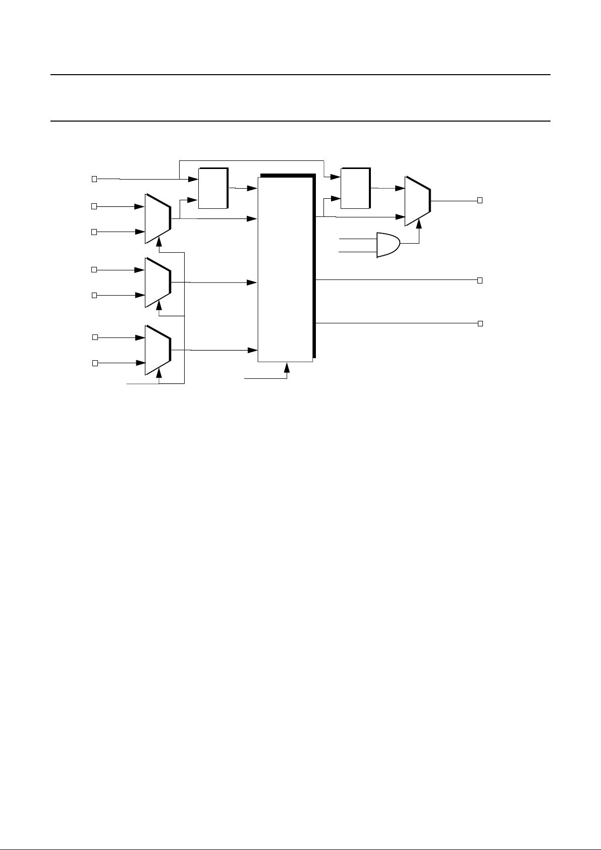
As shown in Figure 1 , the destination
routing memory defines the Local Bus to
SCbus switch connection. There are 128
destination routing memory locations
— one for each Local Bus input channel.
The data stored in the destination routing memory selects the timeslot and
SCbus serial port connection for the
Local Bus input channel. The source
routing memory defines the SCbus to
Local Bus switch connection. There are
128 source routing memory locations —
one for each Local Bus output channel.
The data stored in the source routing
memory selects the time slot and SCbus
serial port connection for the Local Bus
output channel.
2000 Sep 07 12

Philips Semiconductors Preliminary specification
Universal Timeslot Interchange SC4000
Writing to the routing memory is synchronized with SCbus timing. So routing information can be changed only on
time slot boundaries. All input data is
buffered in holding registers. The entire
holding register is transferred to the output registers on a frame boundary basis.
All frame-bounded time slots incur a
one frame delay as they pass through the
switch. Switching data in this fashion
supports time slot bundling.
The SO outputs are tri-state controlled
on time slot boundaries by the Source
Routing Memory Switch Output Enable
Bit. This allows SO outputs from multiple devices to be connected to a common line. The data sample position of
both the SCbus and the Local bus can be
selected for either 50% or 75% of the bit
cell.
In addition to switching local bus serial
data to and from the SCbus, the SC4000
provides a means of switching parallel
data through the microprocessor interface to the SCbus. A frame boundary interrupt helps control the timing of
parallel data accesses. Direct reading and
writing of parallel access register contents makes for an efficient data transfer.
When using direct access, the controlling processor places the address of the
target channel on the address bus. In
this way, data can be read or written in a
single cycle. To avoid data corruption,
the application should not access the
channel for a time period defined as four
clocks before and four clocks after the
frame boundary.
The Source Routing Memory Local
Connect Enable mode allows the switching of any destination channel to
Figure 1. Destination and Source Switch Function Block
1 OF 128 DESTINATION SWITCH
SI_[3:0]
D_[7:0]
W/R_N
INPUT
HOLDING
REGISTER
PARALLEL
ACCESS
REGISTER
O
I
PARALLEL
ACCESS
ENABLE
OUTPUT
HOLDING REGISTER
any source channel without SCbus
intervention. This mode accommodates
either serial or parallel data transfer.
Since data passes through the switch
twice in this mode, there is a two-frame
delay from input to output.
Diagnostic mode electrically disconnects
the SC4000 from the SCbus but allows
access through the local bus. This mode
is particularly useful for running board
diagnostics without upsetting the
SCbus. A Master Clock source is
required to run this mode.
The SC4000 pinout anticipates a future
version of the chip that includes an internal HDLC controller for the message
channel. To remain compatible with this
and other subsequent versions of the
SC4000, applications must write 0 to
all “Reserved (read only)” configuration
registers.
SD_[15:0]
TIMESLOT & PORT
OUTPUT ENABLE
LOCAL CONNECT BUS
DESTINATION
ROUTING MEMORY
1 OF 128 SOURCE SWITCH
OUTPUT
HOLDING
REGISTER
HOLDING
REGISTER
SO_[3:0]
SOURCE
ROUTING MEMORY
INTERNAL PARALLEL
ACCESS
READ
OUTPUT
ENABLE
2000 Sep 07 13
INPUT
TIMESLOT,
PORT AND LOCAL
CONNECT ENABLE

Philips Semiconductors Preliminary specification
Universal Timeslot Interchange SC4000
FUNCTION DESCRIPTION
Switching
The SC4000 allows data switching
through the microprocessor interface in
any of the following three directions:
• From any local bus serial channel (SI)
or parallel data bus D_[7:0] input to
any SCbus channel (SD) output
• From any SCbus channel (SD) input
to any output of the local bus serial
channel (SO) or parallel data bus
D_[7:0]
• From any of local bus serial channel
(SI) or parallel data bus D_[7:0] input
directly through an internal local
connect bus to any local bus serial
channel (SO) output
As shown in Figure 1, each input SI and
output SO channel is mapped to one of
128 unique locations in the destination
routing memory and source routing
memory, respectively. So data stored in
the destination or source routing memory selects the timeslot and serial port of
the SCbus. All data is buffered through
the input holding register, output holding register or parallel access register for
a switching matrix with one frame delay.
PLL Timing and Clock Control
The SC4000 provides the option of using the internal master PLL (C_43 = 0)
or an external master PLL (C_43 = 1).
As shown in Figure 2, the internal
master PLL generates a clock that is frequency-locked to an 8 KHz reference input of either SREF_8K or REF_8K[3:0].
When the SC4000 is enabled as SCbus
master (C_0 =1), a state machine inside
the SC4000 uses this clock to generate
Figure 2. Internal Master PLL (C_43 = 0) Function Block
EXTERNAL
CRYSTAL or OSC
REF_8K_[3:0]
4, 5, 6, 7
C_[42:40]
X_OUT
1
Master PLL
Reference
8 K Select
X_IN
2
65.536 MHz
SCbus
Clock
Master PLL
C_2
C_[10:8], C_[5:4]
Programmable
Divider
SCLK, SCLKX2N and a “free-running”
FSYNCN signal based on the speed of
the SCbus and the clock frequency. The
internal master PLL runs free when:
• Put into free run mode (ignoring
reference input changes) by control
C_[42:40]
• The 8 KHz reference input is static
“1” or “0”
• The input of X_IN is less than 65.536
MHz.
The internal master PLL can also generate an interrupt if it cannot lock the
selected 8 KHz reference input.
C_0, C_3, C_[23:22]
SCLKX2N
SCLKX2NA
46, 47
FSYNCN
FSYNCNA
54, 55
SCLK
SCLKA
49, 50
To Internal Watchdogs and
SCbus Error Detectors
Primary
or
Alternate
C_[45:44]
SCbus
SREF_8K
Source
Select
Select
C_3, C_23, C_46
2000 Sep 07 14
SREF_8K
SREF_8KA
51, 52

Philips Semiconductors Preliminary specification
Universal Timeslot Interchange SC4000
Figure 3 shows an external master PLL
implementation. The SC4000 provides
the 8 KHz reference output signal
REF_8K_OUT (pin 7) to the external
PLL. This 8 KHz reference signal is
sourced from either REF_8K[1:0] or
SREF_8K. The output of the external
PLL is then routed back to the SC4000
via CLK_IN (pin 6). The master clock
input (CLK_IN) frequency select at
C_[10:8] would then be programmed
for the external PLL frequency.
As shown in Figure 4, the SC4000 also
provides an internal clock PLL and local
bus PLL timing control circuitry for
both SCbus master and slave operations.
The internal clock PLL is used to create
the 4.096 or 8.192 MHz timing slaved to
the SCbus when the local bus is running
faster than the SCbus (i.e., 2.048 MHz at
SCbus, 8.096 MHz at local bus). If the
SCbus is faster or equal to the local bus,
then the SCbus clocks serve as the internal clock and use to create the local bus
clocks as well as message channel clock.
The local bus clock PLL is used to create
a 2.048 MHz L_CLK when:
• Local bus framing mode C_[7:6] is set
to 2.048 Mb/s
• A 65.536 MHz clock is supplied on
X_IN
• The C_29 bit is set to one.
If SCLK stops transitionally such as
during a clock fail condition (CLKFAIL
= 1), then the local bus clock PLL runs
free to generate L_CLK clock. In addition, the local bus SO lines are tri-stated
so that the network interface can continue to run.
Interrupts Control
The SC4000 can interrupt the host CPU
with the interrupt request signal INT_0
Figure 3. External Master PLL (C_43 = 1) Function Block
REF_8K_OUT
External
PLL
7
REF_8K_[1:0]
4, 5
C_[42:40]
Master PLL
Reference
8 K Select
(pin 14). This signal is configured and
unmasked by configuration register bits
C_55, C_54 and C_53. The interrupt
sources are:
• C_56 SCbus CLKFAIL
• C_57 Frame Boundary
• C_58 Internal Master PLL Error
• C_59 SCbus Error Indicator (logical
“OR” of C_[67:64], C_[74:72], and
C_[83:80])
The interrupts are structured this way to
improve performance by allowing a single read operation (of configuration register byte 7) to determine whether the
SC4000 is the source of the interrupt.
Each of the SC4000 interrupt sources
can be individually masked.
C_0, C_3, C_[23:22]
SCLKX2N
SCLKX2NA
46, 47
FSYNCN
FSYNCNA
54, 55
SCLK
SCLKA
49, 50
C_2
C_[10:8], C_[5:4]
Programmable
Divider
To Internal Watchdogs and
SCbus Error Detectors
CLK_IN
6
Primary
or
Alternate
C_[45:44]
SCbus
SREF_8K
Source
Select
Select
C_3, C_23, C_46
2000 Sep 07 15
SREF_8K
SREF_8KA
51, 52
Philips Semiconductors Preliminary specification
Universal Timeslot Interchange SC4000
Figure 4. Internal PLL and Local Bus PLL Timing Function Block
X_IN
2
SCLK
49
SCLKA
50
SCLKX2N
46
SCLKX2NA
47
FSYNCN
54
FSYNCNA
55
65.536 MHz
C_2
Primary
or
Alternate
Select
Primary
or
Alternate
Select
Primary
or
Alternate
Select
Internal
Clock
PLL
Internal
Timing
Control
State
Machine
C_[7:6], C_[5:4]
Local
Bus
Clock
PLL
C_[7:6]=0X (2.048 Mb/s)
C_29=1
2.048 MHz
1
0
L_CLK
83
L_FS
84
MC_CLK
11
2000 Sep 07 16
 Loading...