

Philips SC28L92A1B Datasheet

INTEGRATED CIRCUITS
SC28L92
3.3V–5.0V Dual Universal Asynchronous
Receiver/Transmitter (DUART)
Product specification
Supersedes data of 1998 Oct 05
IC19 Data Handbook
1999 May 07

Philips Semiconductors Product specification
3.3V–5.0V Dual Universal Asynchronous
Receiver/Transmitter (DUART)
DESCRIPTION
The SC28L92 is a pin and function replacement for the SCC2692
and SC26C92 operating at 3.3 or 5 volts supply with added features
and deeper FIFOs. Its configuration on power up is that of the
SC26C92. Its differences from the 2692 are: 16 charact er receiver, 16
charac ter transmit FIFOs, watch dog timer for each receiver, mode
register 0 is added, extended baud rate and overall faster speeds,
programmable receiver and transmitter interrupts. (Neither the
SC26C92 nor the SCC2692 is being discontinued.)
Pin programming will allow the device to operate with either the
Motorola or Intel bus interface. The bit 3 of the MR0a register allows
the device to operate in an 8 byte FIFO mode if strict compliance
with the SC26C92 FIFO structure is required.
The Philips Semiconductors SC28L92 Dual Universal Asynchronous
Receiver/Transmitter (DUART) is a single-chip CMOS-LSI
communications device that provides two full-duplex asynchronous
receiver/transmitter channels in a single package. It interfaces
directly with microprocessors and may be used in a polled or
interrupt driven system.
The operating mode and data format of each channel can be
programmed independently. Additionally , each receiver and
transmitter can select its operating speed as one of 27 fixed baud
rates; a 16X clock derived from a programmable counter/timer, or an
external 1X or 16X clock. The baud rate generator and counter/timer
can operate directly from a crystal or from external clock inputs. The
ability to independently program the operating speed of the receiver
and transmitter make the DUART particularly attractive for
dual-speed channel applications such as clustered terminal
systems.
Each receiver and transmitter is buffered by 8 or 16 character FIFOs
to minimize the potential of receiver overrun, transmitter underrun
and to reduce interrupt overhead in interrupt driven systems. In
addition, a flow control capability is provided to disable a remote
transmitter when the receiver buffer is full.
Also provided on the SC28L92 are a multipurpose 7-bit input port
and a multipurpose 8-bit output port. These can be used as general
purpose I/O ports or can be assigned specific functions (such as
clock inputs or status/interrupt outputs) under program control.
The SC28L92 is available in two package versions: a 44-pin PLCC
and 44-pin plastic quad flat pack (PQFP).
FEATURES
•3.3 or 5.0 ±10% volt operation
•Dual full-duplex independent asynchronous receiver/transmitters
•16 character FIFOs for each receiver and transmitter
•Pin programming for 68K or 80xxx bus interface
•Programmable data format
– 5 to 8 data bits plus parity
– Odd, even, no parity or force parity
– - 1, 1.5 or 2 stop bits programmable in 1/16-bit increments
SC28L92
•16-bit programmable Counter/Timer
•Programmable baud rate for each receiver and transmitter
selectable from:
– 28 fixed rates: 50 to 230.4k baud
– Other baud rates to MHz at 16X
– Programmable user-defined rates derived from a programmable
counter/timer
– External 1X or 16X clock
•Parity, framing, and overrun error detection
•False start bit detection
•Line break detection and generation
•Programmable channel mode
– Normal (full-duplex)
– Automatic echo
– Local loop back
– Remote loop back
– Multi-drop mode (also called ‘wake-up’ or ‘9-bit’)
•Multi-function 7-bit input port (includes IACKN)
– Can serve as clock or control inputs
– Change of state detection on four inputs
– Inputs have typically >100k pull-up resistors
– Change of state detectors for modem control
•Multi-function 8-bit output port
– Individual bit set/reset capability
– Outputs can be programmed to be status/interrupt signals
– FIFO status for DMA interface
•Versatile interrupt system
– Single interrupt output with eight maskable interrupting
conditions
– Output port can be configured to provide a total of up to six
separate interrupt outputs that may be wire ORed.
– Each FIFO can be programmed for four dif ferent interrupt levels
– Watch dog timer for each receiver
•Maximum data transfer rates:
1X – 1Mb/sec, 16X – 1Mb/sec
•Automatic wake-up mode for multi-drop applications
•Start-end break interrupt/status
•Detects break which originates in the middle of a character
•On-chip crystal oscillator
•Power down mode
•Receiver time-out mode
•Single +3.3V or +5V power supply
•Powers up to emulate SC26C92
1999 May 07 853–2161 21466
2
Philips Semiconductors Product specification
3.3V–5.0V Dual Universal Asynchronous
Receiver/Transmitter (DUART)
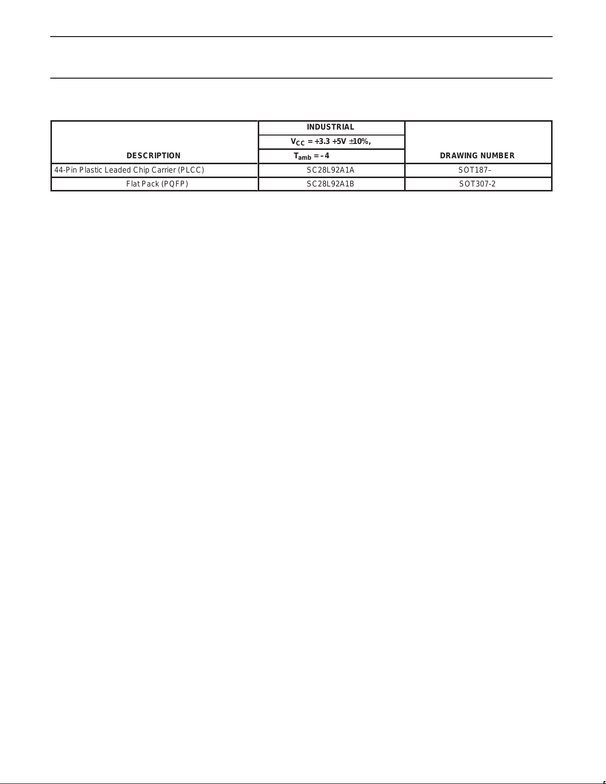
ORDERING INFORMATION
DESCRIPTION
44-Pin Plastic Leaded Chip Carrier (PLCC)
44-Pin Plastic Quad Flat Pack (PQFP)
INDUSTRIAL
VCC = +3.3 +5V ±10%,
T
= –40 to +85°C
amb
SC28L92A1A
SC28L92A1B
SC28L92
DRAWING NUMBER
SOT187–2
SOT307-2
1999 May 07
3

Philips Semiconductors Product specification
3.3V–5.0V Dual Universal Asynchronous
Receiver/Transmitter (DUART)
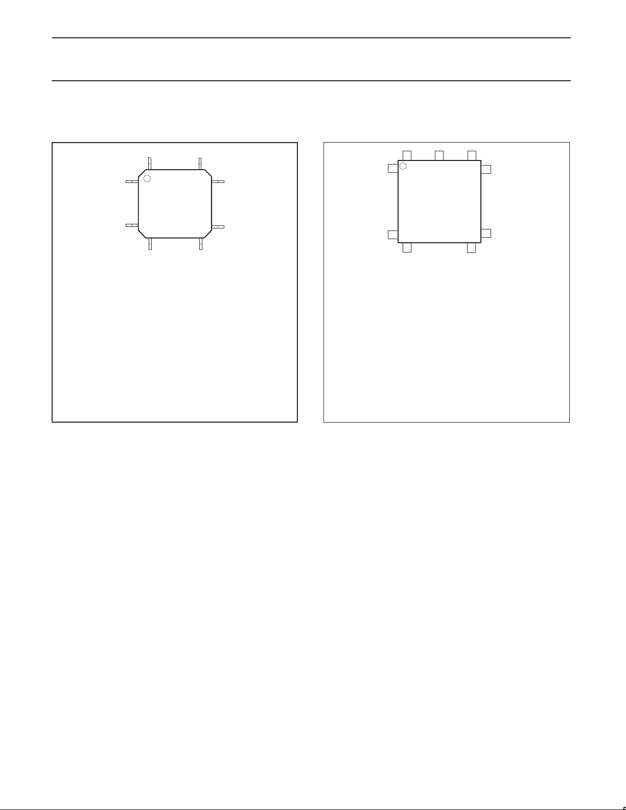
PIN CONFIGURATION DIAGRAM
80XXX PIN CONFIGURA TION
44 34
Pin Function
1A3
2 IP0
3 WRN
4 RDN
5 RxDB
6 TxDB
7 OP1
8 OP3
9 OP5
10 OP7
11 I/M
12 D1
13 D3
14 D5
15 D7
1
PQFP
11
12 22
Pin Function
16 GND
17 GND
18 INTRN
19 D6
20 D4
21 D2
22 D0
23 NC
24 OP6
25 OP4
26 OP2
27 OP0
28 TxDA
29 RxDA
30 x1/clk
33
23
Pin Function
31 x2
32 RESET
33 CEN
34 IP2
35 IP6
36 IP5
37 IP4
38 V
CC
39 V
CC
40 A0
41 IP3
42 A1
43 IP1
44 A2
SD00671
Pin Function
1NC
2A0
3 IP3
4A1
5 IP1
6A2
7A3
8 IP0
9 WRN
10 RDN
11 RxDB
12 I/M
13 TxDB
14 OP1
15 OP3
7
17
6
PLCC
18
Pin Function
16 OP5
17 OP7
18 D1
19 D3
20 D5
21 D7
22 V
23 NC
24 INTRN
25 D6
26 D4
27 D2
28 D0
29 OP6
30 OP4
SC28L92
1
40
39
29
28
Pin Function
31 OP2
32 OP0
33 TxDA
34 NC
35 RxDA
36 X1/CLK
SS
37 X2
38 RESET
39 CEN
40 IP2
41 IP6
42 IP5
43 IP4
44 V
CC
SD00672
1999 May 07
4
Philips Semiconductors Product specification
3.3V–5.0V Dual Universal Asynchronous
Receiver/Transmitter (DUART)
PIN CONFIGURATION DIAGRAM
68XXX PIN CONFIGURA TION
44 34
Pin Function
1A3
2 IP0
3 R/WN
4 DACKN
5 RxDB
6 TxDB
7 OP1
8 OP3
9 OP5
10 OP7
11 I/M
12 D1
13 D3
14 D5
15 D7
1
PQFP
11
12 22
Pin Function
16 GND
17 GND
18 INTRN
19 D6
20 D4
21 D2
22 D0
23 NC
24 OP6
25 OP4
26 OP2
27 OP0
28 TxDA
29 RxDA
30 x1/clk
33
23
Pin Function
31 x2
32 RESETN
33 CSN
34 IP2
35 IACKN
36 IP5
37 IP4
38 V
CC
39 V
CC
40 A0
41 IP3
42 A1
43 IP1
44 A2
SD00673
Pin Function
1NC
2A0
3 IP3
4A1
5 IP1
6A2
7A3
8 IP0
9 R/WN
10 DACKN
11 RxDB
12 I/M
13 TxDB
14 OP1
15 OP3
7
17
6
PLCC
18
Pin Function
16 OP5
17 OP7
18 D1
19 D3
20 D5
21 D7
22 V
23 NC
24 INTRN
25 D6
26 D4
27 D2
28 D0
29 OP6
30 OP4
SC28L92
1
40
39
29
28
Pin Function
31 OP2
32 OP0
33 TxDA
34 NC
35 RxDA
36 X1/CLK
SS
37 X2
38 RESETN
39 CEN
40 IP2
41 IACKN
42 IP5
43 IP4
44 V
CC
SD00674
1999 May 07
5
Philips Semiconductors Product specification
3.3V–5.0V Dual Universal Asynchronous
Receiver/Transmitter (DUART)
8
D0–D7
RDN
WRN
CEN
A0–A3
RESET
INTRN
4
BUS BUFFER
OPERATION CONTROL
ADDRESS
DECODE
R/W CONTROL
INTERRUPT CONTROL
IMR
ISR
GP
CHANNEL A
16 BYTE TRANSMIT
FIFO
TRANSMIT
SHIFT REGISTER
16 BYTE RECEIVE
FIFO
WATCH DOG TIMER
RECEIVE SHIFT
REGISTER
MRA0, 1, 2
CRA
SRA
CHANNEL B
(AS ABOVE)
SC28L92
TxDA
RxDA
TxDB
RxDB
X1/CLK
X2
TIMING
BAUD RATE
GENERATOR
CLOCK
SELECTORS
COUNTER/
TIMER
XTAL OSC
CSRA
CSRB
ACR
CTL
CTU
CONTROL
TIMING
INTERNAL DATABUS
Figure 1. Block Diagram (80XXX mode)
INPUT PORT
CHANGE OF
STATE
DETECTORS (4)
IPCR
ACR
OUTPUT PORT
FUNCTION
SELECT LOGIC
OPCR
OPR
7
8
IP0-IP6
OP0-OP7
V
CC
V
SS
SD00685
1999 May 07
6

Philips Semiconductors Product specification
3.3V–5.0V Dual Universal Asynchronous
Receiver/Transmitter (DUART)
8
D0–D7
R/WN
CEN
A0–A3
RESETN
INTRN
DACKN
4
BUS BUFFER
OPERATION CONTROL
ADDRESS
DECODE
R/W CONTROL
INTERRUPT CONTROL
IMR
ISR
IVR
CHANNEL A
16 BYTE TRANSMIT
FIFO
TRANSMIT
SHIFT REGISTER
16 BYTE RECEIVE
FIFO
WATCH DOG TIMER
RECEIVE SHIFT
REGISTER
MRA0, 1, 2
CRA
SRA
CHANNEL B
(AS ABOVE)
SC28L92
TxDA
RxDA
TxDB
RxDB
X1/CLK
X2
TIMING
BAUD RATE
GENERATOR
CLOCK
SELECTORS
COUNTER/
TIMER
XTAL OSC
CSRA
CSRB
ACR
CTL
CTU
CONTROL
TIMING
INTERNAL DATABUS
Figure 2. Block Diagram (68XXX mode)
INPUT PORT
CHANGE OF
STATE
DETECTORS (4)
IPCR
ACR
OUTPUT PORT
FUNCTION
SELECT LOGIC
OPCR
OPR
6
8
IP0-IP6
IACKN
OP0-OP7
V
CC
V
SS
SD00686
1999 May 07
7

Philips Semiconductors Product specification
Á
Á
Á
Á
Á
Á
Á
Á
Á
Á
Á
Á
Á
Á
Á
Á
Á
Á
Á
Á
Á
Á
Á
Á
Á
Á
Á
Á
Á
Á
Á
Á
Á
3.3V–5.0V Dual Universal Asynchronous
Receiver/Transmitter (DUART)
PIN CONFIGURATION FOR 80XXX BUS INTERFACE (INTEL)
ÁÁ
SYMBOL
I/M
D0–D7
CEN
ÁÁ
WRN
ÁÁ
RDN
A0–A3
RESET
ÁÁ
INTRN
ÁÁ
X1/CLK
X2
ÁÁ
RxDA
RxDB
TxDA
ÁÁ
TxDB
OP0
ÁÁ
OP1
OP2
OP3
ÁÁ
OP4
OP5
OP6
OP7
IP0
IP1
IP2
IP3
ÁÁ
IP4
IP5
ÁÁ
IP6
V
CC
GND
PIN
Á
TYPE
I
I/O
I
Á
I
Á
I
I
I
Á
O
Á
I
O
Á
I
I
O
Á
O
O
Á
O
O
O
Á
O
O
O
O
I
I
I
I
Á
I
I
Á
I
Pwr
Pwr
БББББББББББББББББББББББББББ
NAME AND FUNCTION
Bus Configuration: When high or not connected configures the bus interface to the Conditions shown in this table.
Data Bus: Bi-directional 3-State data bus used to transfer commands, data and status between the DUART and the
CPU. D0 is the least significant bit.
Chip Enable: Active-Low input signal. When Low, data transfers between the CPU and the DUART are enabled on
D0–D7 as controlled by the WRN, RDN and A0–A3 inputs. When High, places the D0–D7 lines in the 3-State
БББББББББББББББББББББББББББ
condition.
Write Strobe: When Low and CEN is also Low, the contents of the data bus is loaded into the addressed register. The
БББББББББББББББББББББББББББ
transfer occurs on the rising edge of the signal.
Read Strobe: When Low and CEN is also Low, causes the contents of the addressed register to be presented on the
data bus. The read cycle begins on the falling edge of RDN.
Address Inputs: Select the DUART internal registers and ports for read/write operations.
Reset: A High level clears internal registers (SRA, SRB, IMR, ISR, OPR, OPCR), puts OP0–OP7 in the High state,
stops the counter/timer, and puts Channels A and B in the inactive state, with the TxDA and TxDB outputs in the mark
БББББББББББББББББББББББББББ
(High) state. Sets MR pointer to MR1.
Interrupt Request: Active-Low, open-drain, output which signals the CPU that one or more of the eight maskable
interrupting conditions are true.
БББББББББББББББББББББББББББ
Crystal 1: Crystal or external clock input. A crystal or clock of the specified limits must be supplied at all times. When a
crystal is used, a capacitor must be connected from this pin to ground (see Figure 7).
Crystal 2: Connection for other side of the crystal. When a crystal is used, a capacitor must be connected from this pin
to ground (see Figure 7). If X1/CLK is driven from an external source, this pin must be left open.
БББББББББББББББББББББББББББ
Channel A Receiver Serial Data Input: The least significant bit is received first. “Mark” is High; “space” is Low.
Channel B Receiver Serial Data Input: The least significant bit is received first. “Mark” is High; “space” is Low.
Channel A Transmitter Serial Data Output: The least significant bit is transmitted first. This output is held in the “mark”
БББББББББББББББББББББББББББ
condition when the transmitter is disabled, idle or when operating in local loop back mode. “Mark” is High; “space” is Low.
Channel B Transmitter Serial Data Output: The least significant bit is transmitted first. This output is held in the ‘mark’
condition when the transmitter is disabled, idle, or when operating in local loop back mode. ‘Mark’ is High; ‘space’ is Low.
Output 0: General purpose output or Channel A request to send (RTSAN, active-Low). Can be deactivated
automatically on receive or transmit.
БББББББББББББББББББББББББББ
Output 1: General-purpose output or Channel B request to send (RTSBN, active-Low). Can be deactivated
automatically on receive or transmit.
Output 2: General purpose output, or Channel A transmitter 1X or 16X clock output, or Channel A receiver 1X clock output.
Output 3: General purpose output or open-drain, active-Low counter/timer output or Channel B transmitter 1X clock
output, or Channel B receiver 1X clock output.
БББББББББББББББББББББББББББ
Output 4: General purpose output or Channel A open-drain, active-Low, RxA interrupt ISR[1] output.
Output 5: General-purpose output or Channel B open-drain, active-Low, RxB interrupt ISR[5] output.
Output 6: General purpose output or Channel A open-drain, active-Low, TxA interrupt ISR[0] output.
Output 7: General-purpose output, or Channel B open-drain, active-Low, TxB interrupt ISR[4] output.
Input 0: General purpose input or Channel A clear to send active-Low input (CTSAN).
Input 1: General purpose input or Channel B clear to send active-Low input (CTSBN).
Input 2: General-purpose input or counter/timer external clock input.
Input 3: General purpose input or Channel A transmitter external clock input (TxCA). When the external clock is used
БББББББББББББББББББББББББББ
by the transmitter, the transmitted data is clocked on the falling edge of the clock.
Input 4: General purpose input or Channel A receiver external clock input (RxCA). When the external clock is used by
the receiver, the received data is sampled on the rising edge of the clock.
Input 5: General purpose input or Channel B transmitter external clock input (TxCB). When the external clock is used
БББББББББББББББББББББББББББ
by the transmitter, the transmitted data is clocked on the falling edge of the clock.
Input 6: General purpose input or Channel B receiver external clock input (RxCB). When the external clock is used by
the receiver, the received data is sampled on the rising edge of the clock.
Power Supply: +3.3 or +5V supply input ±10%
Ground
SC28L92
1999 May 07
8

Philips Semiconductors Product specification
Á
Á
Á
Á
Á
Á
Á
Á
Á
Á
Á
Á
Á
Á
Á
Á
Á
Á
Á
Á
Á
Á
Á
Á
Á
Á
Á
Á
Á
Á
3.3V–5.0V Dual Universal Asynchronous
Receiver/Transmitter (DUART)
PIN CONFIGURATION FOR 68XXX BUS INTERFACE (MOTOROLA)
ÁÁ
SYMBOL
I/M
D0–D7
CSN
ÁÁ
R/WN
IACKN
DACKN
ÁÁ
A0–A3
RESETN
ÁÁ
INTRN
X1/CLK
ÁÁ
X2
RxDA
RxDB
TxDA
ÁÁ
TxDB
OP0
ÁÁ
OP1
OP2
ÁÁ
OP3
OP4
OP5
OP6
OP7
IP0
IP1
IP2
IP3
ÁÁ
IP4
IP5
ÁÁ
V
CC
GND
PIN
Á
TYPE
I
I/O
I
Á
I
I
O
Á
I
I
Á
O
I
Á
O
I
I
O
Á
O
O
Á
O
O
Á
O
O
O
O
O
I
I
I
I
Á
I
I
Á
Pwr
Pwr
БББББББББББББББББББББББББББ
NAME AND FUNCTION
Bus Configuration: When low configures the bus interface to the Conditions shown in this table.
Data Bus: Bi-directional 3-State data bus used to transfer commands, data and status between the DUART and the
CPU. D0 is the least significant bit.
Chip Enable: Active-Low input signal. When Low, data transfers between the CPU and the DUART are enabled on
БББББББББББББББББББББББББББ
D0–D7 as controlled by the R/WN and A0–A3 inputs. When High, places the D0–D7 lines in the 3-State condition.
Read/Write: Input Signal. When CSN is low R/WN high input indicates a read cycle; when low indicates a write cycle.
Interrupt Acknowledge: Active low input indicating an interrupt acknowledge cycle. Usually asserted by the CPU in
response to an interrupt request. When asserted places the interrupt vector on the bus and asserts DACKN.
Data Transfer Acknowledge: A3-State active -low output asserted in a write, read, or interrupt acknowledge cycle to
indicate proper transfer of data between the CPU and the DUART.
БББББББББББББББББББББББББББ
Address Inputs: Select the DUART internal registers and ports for read/write operations.
Reset: A low level clears internal registers (SRA, SRB, IMR, ISR, OPR, OPCR), puts OP0–OP7 in the High state,
stops the counter/timer, and puts Channels A and B in the inactive state, with the TxDA and TxDB outputs in the mark
(High) state. Sets MR pointer to MR1.
БББББББББББББББББББББББББББ
Interrupt Request: Active-Low, open-drain, output which signals the CPU that one or more of the eight maskable
interrupting conditions are true.
Crystal 1: Crystal or external clock input. A crystal or clock of the specified limits must be supplied at all times. When
a crystal is used, a capacitor must be connected from this pin to ground (see Figure 7).
БББББББББББББББББББББББББББ
Crystal 2: Connection for other side of the crystal. When a crystal is used, a capacitor must be connected from this
pin to ground (see Figure 7). If X1/CLK is driven from an external source, this pin must be left open.
Channel A Receiver Serial Data Input: The least significant bit is received first. “Mark” is High, “space” is Low.
Channel B Receiver Serial Data Input: The least significant bit is received first. “Mark” is High, “space” is Low.
Channel A Transmitter Serial Data Output: The least significant bit is transmitted first. This output is held in the “mark”
condition when the transmitter is disabled, idle or when operating in local loop back mode. “Mark” is High; “space” is Low.
БББББББББББББББББББББББББББ
Channel B Transmitter Serial Data Output: The least significant bit is transmitted first. This output is held in the ‘mark’
condition when the transmitter is disabled, idle, or when operating in local loop back mode. ‘Mark’ is High; ‘space’ is Low.
Output 0: General purpose output or Channel A request to send (RTSAN, active-Low). Can be deactivated
automatically on receive or transmit.
БББББББББББББББББББББББББББ
Output 1: General-purpose output or Channel B request to send (RTSBN, active-Low). Can be deactivated
automatically on receive or transmit.
Output 2: General purpose output, or Channel A transmitter 1X or 16X clock output, or Channel A receiver 1X clock
output.
БББББББББББББББББББББББББББ
Output 3: General purpose output or open-drain, active-Low counter/timer output or Channel B transmitter 1X clock
output, or Channel B receiver 1X clock output.
Output 4: General purpose output or Channel A open-drain, active-Low, RxA interrupt ISR [1] output.
Output 5: General-purpose output or Channel B open-drain, active-Low, RxB interrupt ISR[5] output.
Output 6: General purpose output or Channel A open-drain, active-Low, TxA interrupt ISR[0] output.
Output 7: General-purpose output, or Channel B open-drain, active-Low, TxB interrupt ISR[4] output.
Input 0: General purpose input or Channel A clear to send active-Low input (CTSAN).
Input 1: General purpose input or Channel B clear to send active-Low input (CTSBN).
Input 2: General-purpose input or counter/timer external clock input.
Input 3: General purpose input or Channel A transmitter external clock input (TxCA). When the external clock is used
by the transmitter, the transmitted data is clocked on the falling edge of the clock.
БББББББББББББББББББББББББББ
Input 4: General purpose input or Channel A receiver external clock input (RxCA). When the external clock is used by
the receiver, the received data is sampled on the rising edge of the clock.
Input 5: General purpose input or Channel B transmitter external clock input (TxCB). When the external clock is used
by the transmitter, the transmitted data is clocked on the falling edge of the clock.
БББББББББББББББББББББББББББ
Power Supply: +3.3 or +5V supply input ±10%
Ground
SC28L92
1999 May 07
9

Philips Semiconductors Product specification
3.3V–5.0V Dual Universal Asynchronous
Receiver/Transmitter (DUART)
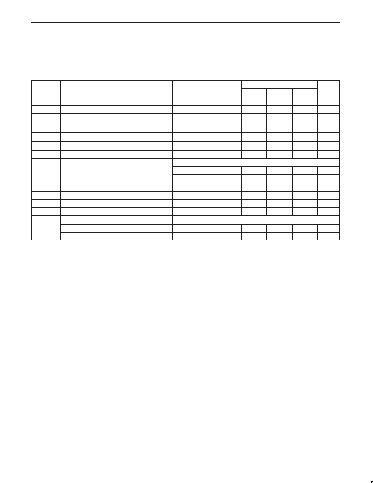
ABSOLUTE MAXIMUM RATINGS
SYMBOL
T
T
V
V
P
P
amb
stg
CC
S
D
D
Operating ambient temperature range
Storage temperature range –65 to +150 °C
Voltage from VCC to GND
Voltage from any pin to GND
Package power dissipation (PLCC44) 2.4 W
Package power dissipation (PQFP44) 1.78 W
Derating factor above 25C (PLCC44)
Derating factor above 25C (PQFP44)
NOTES:
1. Stresses above those listed under Absolute Maximum Ratings may cause permanent damage to the device. This is a stress rating only and
functional operation of the device at these or any other condition above those indicated in the operation section of this specification is not
implied.
2. For operating at elevated temperatures, the device must be derated based on +150°C maximum junction temperature.
3. This product includes circuitry specifically designed for the protection of its internal devices from damaging effects of excessive static
charge. Nonetheless, it is suggested that conventional precautions be taken to avoid applying any voltages larger than the rated maxima.
4. Parameters are valid over specified temperature and voltage range.
DC ELECTRICAL CHARACTERISTICS
= 5V ± 10%, T
V
CC
SYMBOL PARAMETER TEST CONDITIONS Min Typ Max UNIT
V
IL
V
IH
V
IH
V
OL
V
OH
I
IX1PD
I
ILX1
I
IHX1
I
I
I
OZH
I
OZL
I
ODL
I
ODH
I
CC
NOTES:
1. Parameters are valid over specified temperature and voltage range.
2. All voltage measurements are referenced to ground (GND). For testing, all inputs swing between 0.4V and 3.0V with a transition time of
5ns maximum. For X1/CLK, this swing is between 0.4V and 0.8*VCC. All time measurements are referenced at input voltages of 0.8V and
2.0V and output voltages of 0.8V and 2.0V , as appropriate.
3. Typical values are at +25°C, typical supply voltages, and typical processing parameters.
4. Test conditions for outputs: C
constant current source = 2.6mA.
5. Input port pins have active pull-up transistors that will source a typical 2µA from V
Input port pins at V
6. All outputs are disconnected. Inputs are switching between CMOS levels of V
= –40°C to +85°C, unless otherwise specified.
amb
Input low voltage 0.8 V
Input high voltage (except X1/CLK) 2.4 1.5 V
Input high voltage (X1/CLK) 0.8*V
Output low voltage
Output high voltage (except OD outputs)
X1/CLK input current - power down
X1/CLK input low current - operating VIN = 0 –130 0 µA
X1/CLK input high current - operating VIN = V
Input leakage current:
All except input port pins VIN = 0 to V
Input port pins
Output off current high, 3-State data bus VIN = V
Output off current low , 3-State data bus VIN = 0V –0.5 µA
Open-drain output low current in off-state VIN = 0 –0.5 µA
Open-drain output high current in off-state VIN = V
Power supply current
Operating mode CMOS input levels 7 25 mA
Power down mode CMOS input levels ≤1 5
= 125pF, except open drain outputs. Test conditions for open drain outputs: CL = 125pF,
L
source 0.0µA.
CC
1
PARAMETER RATING UNIT
2
3
3
Note 4 °C
–0.5 to +7.0 V
–0.5 to VCC +0.5 V
19 mW/°C
14 mW/°C
1, 2, 3
LIMITS
2.4 V
CC
I
= 2.4mA
OL
4
5
6
I
= -400µA
OH
V
= 0 to V
IN
VIN = 0 to V
CC
CC
CC
CC
CC
CC
when the input pins are at VSS.
CC
-0.2V and VSS + 0.2V.
CC
V
CC
0.5 0.05 0.5 µA
0 130 µA
–0.5 0.05 +0.5 µA
–8 0.05 +0.5 µA
0.2 0.4 V
-0.5 V
SC28L92
0.5 µA
0.5 µA
A
1999 May 07
10
Philips Semiconductors Product specification
3.3V–5.0V Dual Universal Asynchronous
Receiver/Transmitter (DUART)
DC ELECTRICAL CHARACTERISTICS
= 3.3V ± 10%, T
V
CC
SYMBOL PARAMETER TEST CONDITIONS Min Typ Max UNIT
V
IL
V
IH
V
OL
V
OH
I
IX1PD
I
ILX1
I
IHX1
Input low voltage 0.65 0.2*V
Input high voltage (X1/CLK) 0.8*V
Output low voltage
Output high voltage (except OD outputs)
X1/CLK input current - power down
X1/CLK input low current - operating VIN = 0 –80 0 µA
X1/CLK input high current - operating VIN = V
Input leakage current:
I
I
I
OZH
I
OZL
I
ODL
I
ODH
Output off current high, 3-State data bus VIN = V
Output off current low , 3-State data bus VIN = 0V –0.5 µA
Open-drain output low current in off-state VIN = 0 –0.5 µA
Open-drain output high current in off-state VIN = V
Power supply current
I
CC
NOTES:
1. Parameters are valid over specified temperature and voltage range.
2. All voltage measurements are referenced to ground (GND). For testing, all inputs swing between 0.4V and 3.0V with a transition time of
5ns maximum. For X1/CLK, this swing is between 0.4V and 0.8*VCC. All time measurements are referenced at input voltages of 0.8V and
2.0V and output voltages of 0.8V and 2.0V , as appropriate.
3. Typical values are at +25°C, typical supply voltages, and typical processing parameters.
4. Test conditions for outputs: C
constant current source = 2.6mA.
5. Input port pins have active pull-up transistors that will source a typical 2µA from V
Input port pins at V
6. All outputs are disconnected. Inputs are switching between CMOS levels of V
= –40°C to +85°C, unless otherwise specified.
amb
All except input port pins VIN = 0 to V
Input port pins
5
6
Operating mode CMOS input levels 5 mA
Power down mode CMOS input levels ≤1 5.0
= 125pF, except open drain outputs. Test conditions for open drain outputs: CL = 125pF,
L
source 0.0µA.
CC
1, 2, 3
LIMITS
CC
I
= 2.4mA
OL
4
I
= –400µA
OH
V
= 0 to V
IN
VIN = 0 to V
CC
CC
CC
CC
CC
CC
CC
when the input pins are at VSS.
CC
–0.2V and VSS+0.2V.
VCC–0.5 VCC–0.2 V
–0.5 0.05 +0.5 µA
0 80 µA
–0.5 0.05 +0.5 µA
–8 0.5 +0.5 µA
1.7 V
0.2 0.4 V
SC28L92
CC
0.5 µA
0.5 µA
V
A
1999 May 07
11

Philips Semiconductors Product specification
3.3V–5.0V Dual Universal Asynchronous
Receiver/Transmitter (DUART)
AC CHARACTERISTICS (5 VOL T)
= 5.0V ± 10%, T
V
CC
SYMBOL
Reset Timing (See Figure 4)
t
RES
Reset pulse width
Bus Timing5 (See Figure 5)
t
*AS
t
*AH
t
*CS
t
*CH
t
*RW
t
*DD
t
*DA
t
*DF
t
*DI
t
*DS
t
*DH
t
*RWD
A0–A3 setup time to RDN, WRN Low
A0–A3 hold time from RDN, WRN low
CEN setup time to RDN, WRN low
CEN Hold time from RDN. WRN low
WRN, RDN pulse width (Low time)
Data valid after RDN low (125pF load. See Figure 3 for smaller loads.)
RDN low to data bus active
Data bus floating after RDN or CEN high
RDN or CEN high to data bus invalid
Data bus setup time before WRN or CEN high (write cycle)
Data hold time after WRN high
High time between read and/or write cycles
Port Timing5 (See Figure 10)
t
*PS
t
*PH
t
*PD
Port in setup time before RDN low (Read IP ports cycle)
Port in hold time after RDN high
OP port valid after WRN or CEN high (OPR write cycle)
Interrupt Timing (See Figure 11)
t
*IR
INTRN (or OP3–OP7 when used as interrupts) negated from:
Clock Timing (See Figure 7)
t
*CLK
f
*CLK
f
*CTC
f
*CTC
t
*RX
f
*RX
X1/CLK high or low time
X1/CLK frequency
C/T Clk (IP2) high or low time (C/T external clock input)
C/T Clk (IP2) frequency
RxC high or low time (16X)
RxC Frequency (16X)
RxC Frequency (1x)
t
f
*TX
*TX
TxC High or low time (16X)
TxC frequency (16X)
TxC frequency (1X)
Transmitter Timing, external clock (See Figure 13)
t
*TXD
t
*TCS
TxD output delay from TxC low (TxC input pin)
Output delay from TxC output pin low to TxD data output
= –40°C to +85°C, unless otherwise specified.
amb
Read RxFIFO (RxRDY/FFULL interrupt)
Write TxFIFO (TxRDY interrupt)
Reset Command (delta break change interrupt)
Stop C/T command (Counter/timer interrupt
Read IPCR (delta input port change interrupt)
Write IMR (Clear of change interrupt mask bit(s))
8
8, 9
8, 9
1, 2, 3
PARAMETER
6
7
5, 7
8
Min
100
10
20
0
0
15
0
0
25
0
15
0
0
30
0.1
30
0
30
0
0
30
0
LIMITS
Typ
18
6
11
15
17
–15
12
–20
–20
40
40
40
40
40
40
40
20
3.686
20
40
6
SC28L92
Max
40
20
60
60
60
60
60
60
60
8.5
8
16
1
16
1
60
30
UNIT
MHz
MHz
MHz
MHz
MHz
MHz
ns
ns
ns
ns
ns
ns
ns
ns
ns
ns
ns
ns
ns
ns
ns
ns
ns
ns
ns
ns
ns
ns
ns
ns
ns
ns
ns
ns
1999 May 07
12

Philips Semiconductors Product specification
3.3V–5.0V Dual Universal Asynchronous
Receiver/Transmitter (DUART)
LIMITS
Typ
SYMBOL
SYMBOL
PARAMETER
PARAMETER
Receiver Timing, external clock (See Figure 14)
t
*RXS
t
*RXH
68000 or Motorola bus timing (See Figures 7, 8, 9)
t
DCR
t
DCW
t
DAT
t
CSC
RxD data setup time to RxC high
RxD data hold time from RxC high
10
DACKN Low (read cycle) from X1 High
10
DACKN Low (write cycle) from X1 High
DACKN High impedance from CSN or IACKN High
CSN or IACKN setup time to X1 High for minimum DACKN cycle
NOTES:
1. Parameters are valid over specified temperature and voltage range.
2. All voltage measurements are referenced to ground (GND). For testing, all inputs swing between 0.4 V and 3.0 V with a transition time of
5 ns maximum. For X1/CLK this swing is between 0.4 V and 0.8*V
2.0 V and output voltages of 0.8 V and 2.0 V , as appropriate.
. All time measurements are referenced at input voltages of 0.8 V and
CC
3. Test conditions for outputs: CL = 125 pF, except open drain outputs. Test conditions for open drain outputs: C
constant current source = 2.6mA.
4. Typical values are at +25°C, typical supply voltages, and typical processing parameters.
5. Timing is illustrated and referenced to the WRN and RDN Inputs. Also, CEN may be the “strobing” input. CEN and RDN (also CEN and
WRN) are ORed internally. The signal asserted last initiates the cycle and the signal negated first terminates the cycle.
6. Guaranteed by characterization of sample units.
7. If CEN is used as the “strobing” input, the parameter defines the minimum High times between one CEN and the next. The RDN signal must
be negated for t
8. Minimum frequencies are not tested but are guaranteed by design.
to guarantee that any status register changes are valid.
RWD
9. Clocks for 1X mode should maintain a 60/40 duty cycle or better.
= t
+ t
10.Minimum DACKN time is t
while in the 68XXX mode. It is not necessary to wait for DACKN to insure the proper operation of the SC28C92. In all cases the data will be
DCR
DSC
+ two positive edges of the X1 clock. For faster bus cycles, the 80XXX bus timing may be used
DCR
written to the SC28L92 on the falling edge of DACKN or the rise of CEN or WRN, which ever of the three occurs first.
Min
50
50
10
40
40
15
15
8
8
= 125 pF,
L
SC28L92
Max
20
20
10
UNIT
UNIT
ns
ns
ns
ns
ns
ns
85
80
75
70
65
60
55
50
45
T
dd
(ns)
40
35
30
25
20
15
10
5
0
0 20 40 60 80 100 120 140 160 180 200 220 240
NOTES:
3.3V operation adds 40% to these times.
Bus cycle times:
(80XXX mode): t
(68XXX mode) = t
RW
+ t
CSC
RWD
+ t
DAT
125 pF 152 pF 225 pF
pF
= 30ns @ 5V, 40ns @ 3.3V + rise and fall time of control signals
+ 1 X1 clock cycle @ 5V + rise and fall time of control signals
Figure 3. Port Timing vs. Capacitive Loading
4.5V @ +85°C
5.5V @ +25°C
SD00684
1999 May 07
13

Philips Semiconductors Product specification
3.3V–5.0V Dual Universal Asynchronous
Receiver/Transmitter (DUART)
AC CHARACTERISTICS (3.3 VOL T)
= 3.3V ± 10%, T
V
CC
SYMBOL
Reset Timing (See Figure 4)
t
RES
Reset pulse width
Bus Timing5 (See Figure 5)
t
*AS
t
*AH
t
*CS
t
*CH
t
*RW
t
*DD
t
*DA
t
*DF
t
*DI
t
*DS
t
*DH
t
*RWD
A0–A3 setup time to RDN, WRN Low
A0–A3 hold time from RDN, WRN low
CEN setup time to RDN, WRN low
CEN Hold time from RDN. WRN low
WRN, RDN pulse width (Low time)
Data valid after RDN low (125pF load. See Figure 3 for smaller loads.)
RDN low to data bus active
Data bus floating after RDN or CEN high
RDN or CEN high to data bus invalid
Data bus setup time before WRN or CEN high (write cycle)
Data hold time after WRN high
High time between read and/or write cycles
Port Timing5 (See Figure 10)
t
*PS
t
*PH
t
*PD
Port in setup time before RDN low (Read IP ports cycle)
Port in hold time after RDN high
OP port valid after WRN or CEN high (OPR write cycle)
Interrupt Timing (See Figure 11)
t
*IR
INTRN (or OP3–OP7 when used as interrupts) negated from:
Clock Timing (See Figure 7)
t
*CLK
f
*CLK
f
*CTC
f
*CTC
t
*RX
f
*RX
X1/CLK high or low time
X1/CLK frequency
C/T Clk (IP2) high or low time (C/T external clock input)
C/T Clk (IP2) frequency
RxC high or low time (16X)
RxC Frequency (16X)
RxC Frequency (1x)
t
f
*TX
*TX
TxC High or low time (16X)
TxC frequency (16X)
TxC frequency (1X)
Transmitter Timing, external clock (See Figure 13)
t
*TXD
t
*TCS
TxD output delay from TxC low (TxC input pin)
Output delay from TxC output pin low to TxD data output
= –40°C to +85°C, unless otherwise specified.
amb
Read RxFIFO (RxRDY/FFULL interrupt)
Write TxFIFO (TxRDY interrupt)
Reset Command (delta break change interrupt)
Stop C/T command (Counter/timer interrupt
Read IPCR (delta input port change interrupt)
Write IMR (Clear of change interrupt mask bit(s))
8
8, 9
8, 9
1, 2, 3
PARAMETER
6
7
5, 7
8
Min
100
10
25
0
0
20
0
0
25
0
20
0
0
30
0.1
30
0
30
0
0
30
0
LIMITS
Typ
18
6
15
15
20
15
20
–15
14
–20
–20
50
40
40
40
40
40
40
20
3.686
20
40
6
SC28L92
4
Max
50
20
70
60
60
60
60
60
60
8.5
8
16
1
16
1
60
30
UNIT
ns
ns
ns
ns
ns
ns
ns
ns
ns
ns
ns
ns
ns
ns
ns
ns
ns
ns
ns
ns
ns
ns
ns
MHz
ns
MHz
ns
MHz
MHz
ns
MHz
MHz
ns
ns
1999 May 07
14
 Loading...