

Philips SC28L202A1B, SC28L202A1D Datasheet

INTEGRATED CIRCUITS
SC28L202
Dual universal asynchronous
receiver/transmitter (DUART)
Objective specification
Supersedes data of 2000 Jan 31
IC19 Data Handbook
2000 Feb 10

Philips Semiconductors Objective specification
Dual universal asynchronous receiver/transmitter
(DUART)
DESCRIPTION 1. . . . . . . . . . . . . . . . . . . . . . . . . . . . . . . . . . . . . . . . . . . . . . . . . . . . . . . . . . . . . . . . . . . . . . . . . . . . . . . . . . . . . . . . . . . . . . . . . . . . . . .
FEATURES 1. . . . . . . . . . . . . . . . . . . . . . . . . . . . . . . . . . . . . . . . . . . . . . . . . . . . . . . . . . . . . . . . . . . . . . . . . . . . . . . . . . . . . . . . . . . . . . . . . . . . . . . . . .
ORDERING INFORMATION 2. . . . . . . . . . . . . . . . . . . . . . . . . . . . . . . . . . . . . . . . . . . . . . . . . . . . . . . . . . . . . . . . . . . . . . . . . . . . . . . . . . . . . . . . . . . .
PIN CONFIGURATION FOR 80XXX BUS INTERFACE (INTEL) (PRELIMINARY 2/10/00) 3. . . . . . . . . . . . . . . . . . . . . . . . . . . . . . . . . . . . . .
CONFIGURATION FOR 68XXX BUS INTERFACE (MOTOROLA) 4. . . . . . . . . . . . . . . . . . . . . . . . . . . . . . . . . . . . . . . . . . . . . . . . . . . . . . . . . . .
OVERALL DESCRIPTION 7. . . . . . . . . . . . . . . . . . . . . . . . . . . . . . . . . . . . . . . . . . . . . . . . . . . . . . . . . . . . . . . . . . . . . . . . . . . . . . . . . . . . . . . . . . . . .
BRIEF DESCRIPTION OF FUNCTIONAL BLOCKS 7. . . . . . . . . . . . . . . . . . . . . . . . . . . . . . . . . . . . . . . . . . . . . . . . . . . . . . . . . . . . . . . . . . . . .
Bus Interface 7. . . . . . . . . . . . . . . . . . . . . . . . . . . . . . . . . . . . . . . . . . . . . . . . . . . . . . . . . . . . . . . . . . . . . . . . . . . . . . . . . . . . . . . . . . . . . . . . . . .
Timing Circuits 7. . . . . . . . . . . . . . . . . . . . . . . . . . . . . . . . . . . . . . . . . . . . . . . . . . . . . . . . . . . . . . . . . . . . . . . . . . . . . . . . . . . . . . . . . . . . . . . . . .
I/O ports 7. . . . . . . . . . . . . . . . . . . . . . . . . . . . . . . . . . . . . . . . . . . . . . . . . . . . . . . . . . . . . . . . . . . . . . . . . . . . . . . . . . . . . . . . . . . . . . . . . . . . . . .
UART s 7. . . . . . . . . . . . . . . . . . . . . . . . . . . . . . . . . . . . . . . . . . . . . . . . . . . . . . . . . . . . . . . . . . . . . . . . . . . . . . . . . . . . . . . . . . . . . . . . . . . . . . . . .
Transmitters and Receivers 7. . . . . . . . . . . . . . . . . . . . . . . . . . . . . . . . . . . . . . . . . . . . . . . . . . . . . . . . . . . . . . . . . . . . . . . . . . . . . . . . . . . . . . .
Character and Address Recognition 7. . . . . . . . . . . . . . . . . . . . . . . . . . . . . . . . . . . . . . . . . . . . . . . . . . . . . . . . . . . . . . . . . . . . . . . . . . . . . . . .
Flow Control 8. . . . . . . . . . . . . . . . . . . . . . . . . . . . . . . . . . . . . . . . . . . . . . . . . . . . . . . . . . . . . . . . . . . . . . . . . . . . . . . . . . . . . . . . . . . . . . . . . . . .
Test Modes and Software 8. . . . . . . . . . . . . . . . . . . . . . . . . . . . . . . . . . . . . . . . . . . . . . . . . . . . . . . . . . . . . . . . . . . . . . . . . . . . . . . . . . . . . . . . .
DETAILED DESCRIPTIONS 8. . . . . . . . . . . . . . . . . . . . . . . . . . . . . . . . . . . . . . . . . . . . . . . . . . . . . . . . . . . . . . . . . . . . . . . . . . . . . . . . . . . . . . . . .
Bus Interface 8. . . . . . . . . . . . . . . . . . . . . . . . . . . . . . . . . . . . . . . . . . . . . . . . . . . . . . . . . . . . . . . . . . . . . . . . . . . . . . . . . . . . . . . . . . . . . . . . . . .
Timing Circuit 8. . . . . . . . . . . . . . . . . . . . . . . . . . . . . . . . . . . . . . . . . . . . . . . . . . . . . . . . . . . . . . . . . . . . . . . . . . . . . . . . . . . . . . . . . . . . . . . . . . .
I/O Ports 9. . . . . . . . . . . . . . . . . . . . . . . . . . . . . . . . . . . . . . . . . . . . . . . . . . . . . . . . . . . . . . . . . . . . . . . . . . . . . . . . . . . . . . . . . . . . . . . . . . . . . . .
UART Operation 10. . . . . . . . . . . . . . . . . . . . . . . . . . . . . . . . . . . . . . . . . . . . . . . . . . . . . . . . . . . . . . . . . . . . . . . . . . . . . . . . . . . . . . . . . . . . . . . . . . .
Receiver Operation 11. . . . . . . . . . . . . . . . . . . . . . . . . . . . . . . . . . . . . . . . . . . . . . . . . . . . . . . . . . . . . . . . . . . . . . . . . . . . . . . . . . . . . . . . . . . . . .
Arbitrating Interrupt Structure 14. . . . . . . . . . . . . . . . . . . . . . . . . . . . . . . . . . . . . . . . . . . . . . . . . . . . . . . . . . . . . . . . . . . . . . . . . . . . . . . . . . . . . .
PROGRAMMING THE HOST INTERFACE 19. . . . . . . . . . . . . . . . . . . . . . . . . . . . . . . . . . . . . . . . . . . . . . . . . . . . . . . . . . . . . . . . . . . . . . . . . . . . . . .
REGISTER DESCRIPTION AND PROGRAMMING NOTE 20. . . . . . . . . . . . . . . . . . . . . . . . . . . . . . . . . . . . . . . . . . . . . . . . . . . . . . . . . . . . . . . . . .
Registers that control Global Properties of the 28L202 20. . . . . . . . . . . . . . . . . . . . . . . . . . . . . . . . . . . . . . . . . . . . . . . . . . . . . . . . . . . . . . . . . . .
GCCR – Global Configuration Control Register 20. . . . . . . . . . . . . . . . . . . . . . . . . . . . . . . . . . . . . . . . . . . . . . . . . . . . . . . . . . . . . . . . . . . . . .
GCCR(7:6) DACKN Assertion 20. . . . . . . . . . . . . . . . . . . . . . . . . . . . . . . . . . . . . . . . . . . . . . . . . . . . . . . . . . . . . . . . . . . . . . . . . . . . . . . . . . . . .
GCCR(5:3): Reserved 20. . . . . . . . . . . . . . . . . . . . . . . . . . . . . . . . . . . . . . . . . . . . . . . . . . . . . . . . . . . . . . . . . . . . . . . . . . . . . . . . . . . . . . . . . . . .
GCCR(2:1): Interrupt vector configuration 20. . . . . . . . . . . . . . . . . . . . . . . . . . . . . . . . . . . . . . . . . . . . . . . . . . . . . . . . . . . . . . . . . . . . . . . . . . .
GCCR(0): Interrupt Status Masking 20. . . . . . . . . . . . . . . . . . . . . . . . . . . . . . . . . . . . . . . . . . . . . . . . . . . . . . . . . . . . . . . . . . . . . . . . . . . . . . . .
SFSR A and B Special Feature & Status Register 20. . . . . . . . . . . . . . . . . . . . . . . . . . . . . . . . . . . . . . . . . . . . . . . . . . . . . . . . . . . . . . . . . . . .
SFSR(7:4) Reserved 21. . . . . . . . . . . . . . . . . . . . . . . . . . . . . . . . . . . . . . . . . . . . . . . . . . . . . . . . . . . . . . . . . . . . . . . . . . . . . . . . . . . . . . . . . . . . .
SFSR(3) Status of loop back error check. 21. . . . . . . . . . . . . . . . . . . . . . . . . . . . . . . . . . . . . . . . . . . . . . . . . . . . . . . . . . . . . . . . . . . . . . . . . . .
SFSR(0) Reserved 21. . . . . . . . . . . . . . . . . . . . . . . . . . . . . . . . . . . . . . . . . . . . . . . . . . . . . . . . . . . . . . . . . . . . . . . . . . . . . . . . . . . . . . . . . . . . . .
TRR Test and Revision Register. 21. . . . . . . . . . . . . . . . . . . . . . . . . . . . . . . . . . . . . . . . . . . . . . . . . . . . . . . . . . . . . . . . . . . . . . . . . . . . . . . . . .
TRR(7) Test 2 Enable 21. . . . . . . . . . . . . . . . . . . . . . . . . . . . . . . . . . . . . . . . . . . . . . . . . . . . . . . . . . . . . . . . . . . . . . . . . . . . . . . . . . . . . . . . . . . .
TRR [6:0] – Chip Revision Code 21. . . . . . . . . . . . . . . . . . . . . . . . . . . . . . . . . . . . . . . . . . . . . . . . . . . . . . . . . . . . . . . . . . . . . . . . . . . . . . . . . . .
STCR – Scan Test Control Register. 21. . . . . . . . . . . . . . . . . . . . . . . . . . . . . . . . . . . . . . . . . . . . . . . . . . . . . . . . . . . . . . . . . . . . . . . . . . . . . . .
SES – System Enable Status Register, A and B 21. . . . . . . . . . . . . . . . . . . . . . . . . . . . . . . . . . . . . . . . . . . . . . . . . . . . . . . . . . . . . . . . . . . . .
EOS – Enhanced Operation Status Register 21. . . . . . . . . . . . . . . . . . . . . . . . . . . . . . . . . . . . . . . . . . . . . . . . . . . . . . . . . . . . . . . . . . . . . . . .
UART Registers 22. . . . . . . . . . . . . . . . . . . . . . . . . . . . . . . . . . . . . . . . . . . . . . . . . . . . . . . . . . . . . . . . . . . . . . . . . . . . . . . . . . . . . . . . . . . . . . . . . . . .
These registers are generally concerned with formatting, transmitting and receiving data. 22. . . . . . . . . . . . . . . . . . . . . . . . . . . . . . . . . .
MR0 – Mode Register 0, A and B 22. . . . . . . . . . . . . . . . . . . . . . . . . . . . . . . . . . . . . . . . . . . . . . . . . . . . . . . . . . . . . . . . . . . . . . . . . . . . . . . . . .
MR0[7] Fixed length Watchdog T imer 22. . . . . . . . . . . . . . . . . . . . . . . . . . . . . . . . . . . . . . . . . . . . . . . . . . . . . . . . . . . . . . . . . . . . . . . . . . . . . .
MR0[5:4] – Tx interrupt fill level. 22. . . . . . . . . . . . . . . . . . . . . . . . . . . . . . . . . . . . . . . . . . . . . . . . . . . . . . . . . . . . . . . . . . . . . . . . . . . . . . . . . . .
MR0[3] – FIFO Size 22. . . . . . . . . . . . . . . . . . . . . . . . . . . . . . . . . . . . . . . . . . . . . . . . . . . . . . . . . . . . . . . . . . . . . . . . . . . . . . . . . . . . . . . . . . . . . .
MR0[2:0] – Legacy Baud Rate Group Selection 22. . . . . . . . . . . . . . . . . . . . . . . . . . . . . . . . . . . . . . . . . . . . . . . . . . . . . . . . . . . . . . . . . . . . . .
MR1 – Mode Register 1, A and B 23. . . . . . . . . . . . . . . . . . . . . . . . . . . . . . . . . . . . . . . . . . . . . . . . . . . . . . . . . . . . . . . . . . . . . . . . . . . . . . . . . .
MR1[7] – Receiver Request to Send (hardware flow control) 23. . . . . . . . . . . . . . . . . . . . . . . . . . . . . . . . . . . . . . . . . . . . . . . . . . . . . . . . . . .
MR1[6] – Receiver interrupt control bit 1. 23. . . . . . . . . . . . . . . . . . . . . . . . . . . . . . . . . . . . . . . . . . . . . . . . . . . . . . . . . . . . . . . . . . . . . . . . . . . .
MR1 [5] – Error Mode Select and sub modes 23. . . . . . . . . . . . . . . . . . . . . . . . . . . . . . . . . . . . . . . . . . . . . . . . . . . . . . . . . . . . . . . . . . . . . . . .
MR1[4:3] – Parity Mode Select 23. . . . . . . . . . . . . . . . . . . . . . . . . . . . . . . . . . . . . . . . . . . . . . . . . . . . . . . . . . . . . . . . . . . . . . . . . . . . . . . . . . . .
MR1[2] – Parity Type Select 23. . . . . . . . . . . . . . . . . . . . . . . . . . . . . . . . . . . . . . . . . . . . . . . . . . . . . . . . . . . . . . . . . . . . . . . . . . . . . . . . . . . . . . .
MR1[1:0] – Bits per Character Select 23. . . . . . . . . . . . . . . . . . . . . . . . . . . . . . . . . . . . . . . . . . . . . . . . . . . . . . . . . . . . . . . . . . . . . . . . . . . . . . .
MR2 – Mode Register 2, A and B 24. . . . . . . . . . . . . . . . . . . . . . . . . . . . . . . . . . . . . . . . . . . . . . . . . . . . . . . . . . . . . . . . . . . . . . . . . . . . . . . . . .
MR2[7:6] – Mode Select 24. . . . . . . . . . . . . . . . . . . . . . . . . . . . . . . . . . . . . . . . . . . . . . . . . . . . . . . . . . . . . . . . . . . . . . . . . . . . . . . . . . . . . . . . . .
MR2[7:6] = b’00 Normal Mode 24. . . . . . . . . . . . . . . . . . . . . . . . . . . . . . . . . . . . . . . . . . . . . . . . . . . . . . . . . . . . . . . . . . . . . . . . . . . . . . . . . . . . .
MR2[7:6] = b’01 Automatic Echo 24. . . . . . . . . . . . . . . . . . . . . . . . . . . . . . . . . . . . . . . . . . . . . . . . . . . . . . . . . . . . . . . . . . . . . . . . . . . . . . . . . . .
MR2[7:6] = b’10 selects local loop back diagnostic mode. In this mode: 24. . . . . . . . . . . . . . . . . . . . . . . . . . . . . . . . . . . . . . . . . . . . . . . . .
MR2 [7:6] = b’11 Selects the Remote Loop back diagnostic mode. In this mode: 24. . . . . . . . . . . . . . . . . . . . . . . . . . . . . . . . . . . . . . . . . .
MR2[5] Transmitter Request to Send Control 24. . . . . . . . . . . . . . . . . . . . . . . . . . . . . . . . . . . . . . . . . . . . . . . . . . . . . . . . . . . . . . . . . . . . . . . .
MR2[4] – Clear to Send Control 24. . . . . . . . . . . . . . . . . . . . . . . . . . . . . . . . . . . . . . . . . . . . . . . . . . . . . . . . . . . . . . . . . . . . . . . . . . . . . . . . . . .
MR2[3:0] – Stop Bit Length Select 24. . . . . . . . . . . . . . . . . . . . . . . . . . . . . . . . . . . . . . . . . . . . . . . . . . . . . . . . . . . . . . . . . . . . . . . . . . . . . . . . .
SC28L202
2000 Feb 10
i

Philips Semiconductors Objective specification
Dual universal asynchronous receiver/transmitter
(DUART)
MR3 – Mode Register 3, A and B 25. . . . . . . . . . . . . . . . . . . . . . . . . . . . . . . . . . . . . . . . . . . . . . . . . . . . . . . . . . . . . . . . . . . . . . . . . . . . . . . . . .
MR3[7 & 6] Xon/Xoff Character Stripping 25. . . . . . . . . . . . . . . . . . . . . . . . . . . . . . . . . . . . . . . . . . . . . . . . . . . . . . . . . . . . . . . . . . . . . . . . . . .
MR3[5:4] Reserved 25. . . . . . . . . . . . . . . . . . . . . . . . . . . . . . . . . . . . . . . . . . . . . . . . . . . . . . . . . . . . . . . . . . . . . . . . . . . . . . . . . . . . . . . . . . . . . .
MR3[3:2] Xon/Xoff Processing 25. . . . . . . . . . . . . . . . . . . . . . . . . . . . . . . . . . . . . . . . . . . . . . . . . . . . . . . . . . . . . . . . . . . . . . . . . . . . . . . . . . . . .
MR3[1:0] Address Recognition 25. . . . . . . . . . . . . . . . . . . . . . . . . . . . . . . . . . . . . . . . . . . . . . . . . . . . . . . . . . . . . . . . . . . . . . . . . . . . . . . . . . . .
RxCSR – Receiver Clock Select Register A and B 26. . . . . . . . . . . . . . . . . . . . . . . . . . . . . . . . . . . . . . . . . . . . . . . . . . . . . . . . . . . . . . . . . . .
TxCSR Transmitter Clock Select Register A and B 26. . . . . . . . . . . . . . . . . . . . . . . . . . . . . . . . . . . . . . . . . . . . . . . . . . . . . . . . . . . . . . . . . . .
Rx and Tx Clock Select Table 26. . . . . . . . . . . . . . . . . . . . . . . . . . . . . . . . . . . . . . . . . . . . . . . . . . . . . . . . . . . . . . . . . . . . . . . . . . . . . . . . . . . . .
CRx – Command Register Extension, A and B 27. . . . . . . . . . . . . . . . . . . . . . . . . . . . . . . . . . . . . . . . . . . . . . . . . . . . . . . . . . . . . . . . . . . . . . .
CR[7] – Lock Tx and Rx enables. 27. . . . . . . . . . . . . . . . . . . . . . . . . . . . . . . . . . . . . . . . . . . . . . . . . . . . . . . . . . . . . . . . . . . . . . . . . . . . . . . . . .
WRITES TO THE LOWER 5 BITS OF THE CR WOULD USUALLY HAVE CR[7] 27. . . . . . . . . . . . . . . . . . . . . . . . . . . . . . . . . . . . . . . . .
CR[6] – Enable Transmitter 27. . . . . . . . . . . . . . . . . . . . . . . . . . . . . . . . . . . . . . . . . . . . . . . . . . . . . . . . . . . . . . . . . . . . . . . . . . . . . . . . . . . . . . .
CR[5] – Enable Receiver 27. . . . . . . . . . . . . . . . . . . . . . . . . . . . . . . . . . . . . . . . . . . . . . . . . . . . . . . . . . . . . . . . . . . . . . . . . . . . . . . . . . . . . . . . .
CR[4:0] – Miscellaneous Commands (See Table below) 27. . . . . . . . . . . . . . . . . . . . . . . . . . . . . . . . . . . . . . . . . . . . . . . . . . . . . . . . . . . . . . .
COMMAND REGISTER EXTENSION TABLE A and B 28. . . . . . . . . . . . . . . . . . . . . . . . . . . . . . . . . . . . . . . . . . . . . . . . . . . . . . . . . . . . . . . .
SR – Channel Status Register A and B 29. . . . . . . . . . . . . . . . . . . . . . . . . . . . . . . . . . . . . . . . . . . . . . . . . . . . . . . . . . . . . . . . . . . . . . . . . . . . .
SR[7] – Received Break 29. . . . . . . . . . . . . . . . . . . . . . . . . . . . . . . . . . . . . . . . . . . . . . . . . . . . . . . . . . . . . . . . . . . . . . . . . . . . . . . . . . . . . . . . . .
SR[6] – Framing Error (FE) 29. . . . . . . . . . . . . . . . . . . . . . . . . . . . . . . . . . . . . . . . . . . . . . . . . . . . . . . . . . . . . . . . . . . . . . . . . . . . . . . . . . . . . . .
SR[5] – Parity Error (PE) 29. . . . . . . . . . . . . . . . . . . . . . . . . . . . . . . . . . . . . . . . . . . . . . . . . . . . . . . . . . . . . . . . . . . . . . . . . . . . . . . . . . . . . . . . .
SR[4] – Overrun Error (OE) 29. . . . . . . . . . . . . . . . . . . . . . . . . . . . . . . . . . . . . . . . . . . . . . . . . . . . . . . . . . . . . . . . . . . . . . . . . . . . . . . . . . . . . . .
SR [3] – Transmitter Idle (Tx Idle) 29. . . . . . . . . . . . . . . . . . . . . . . . . . . . . . . . . . . . . . . . . . . . . . . . . . . . . . . . . . . . . . . . . . . . . . . . . . . . . . . . . .
SR[2] – Transmitter Ready (TxRDY) 29. . . . . . . . . . . . . . . . . . . . . . . . . . . . . . . . . . . . . . . . . . . . . . . . . . . . . . . . . . . . . . . . . . . . . . . . . . . . . . .
SR[1] – RxFIFO Full (RxFULL) 29. . . . . . . . . . . . . . . . . . . . . . . . . . . . . . . . . . . . . . . . . . . . . . . . . . . . . . . . . . . . . . . . . . . . . . . . . . . . . . . . . . . .
SR[0] – Receiver Ready (RxRDY) 29. . . . . . . . . . . . . . . . . . . . . . . . . . . . . . . . . . . . . . . . . . . . . . . . . . . . . . . . . . . . . . . . . . . . . . . . . . . . . . . . .
ISR – Interrupt Status Register A and B 30. . . . . . . . . . . . . . . . . . . . . . . . . . . . . . . . . . . . . . . . . . . . . . . . . . . . . . . . . . . . . . . . . . . . . . . . . . . .
ISR[7] – Input Change of State. 30. . . . . . . . . . . . . . . . . . . . . . . . . . . . . . . . . . . . . . . . . . . . . . . . . . . . . . . . . . . . . . . . . . . . . . . . . . . . . . . . . . . .
ISR[6] Fixed Watchdog Time–out. 30. . . . . . . . . . . . . . . . . . . . . . . . . . . . . . . . . . . . . . . . . . . . . . . . . . . . . . . . . . . . . . . . . . . . . . . . . . . . . . . . .
ISR[5] – Address Recognition Status Change. 30. . . . . . . . . . . . . . . . . . . . . . . . . . . . . . . . . . . . . . . . . . . . . . . . . . . . . . . . . . . . . . . . . . . . . . .
ISR[4] – Xon/Xoff Status Change. 30. . . . . . . . . . . . . . . . . . . . . . . . . . . . . . . . . . . . . . . . . . . . . . . . . . . . . . . . . . . . . . . . . . . . . . . . . . . . . . . . . .
ISR[3] – Counter Timer Status 30. . . . . . . . . . . . . . . . . . . . . . . . . . . . . . . . . . . . . . . . . . . . . . . . . . . . . . . . . . . . . . . . . . . . . . . . . . . . . . . . . . . . .
ISR[2] – Change in Channel Break Status. 30. . . . . . . . . . . . . . . . . . . . . . . . . . . . . . . . . . . . . . . . . . . . . . . . . . . . . . . . . . . . . . . . . . . . . . . . . .
ISR[1] – RxINT. (Also Rx DMA hand shake at I/O pins) 30. . . . . . . . . . . . . . . . . . . . . . . . . . . . . . . . . . . . . . . . . . . . . . . . . . . . . . . . . . . . . . .
ISR[0] – TxINT. (Also Tx DMA hand shake at I/O pins) 30. . . . . . . . . . . . . . . . . . . . . . . . . . . . . . . . . . . . . . . . . . . . . . . . . . . . . . . . . . . . . . . .
IMR – Interrupt Mask Register A and B 31. . . . . . . . . . . . . . . . . . . . . . . . . . . . . . . . . . . . . . . . . . . . . . . . . . . . . . . . . . . . . . . . . . . . . . . . . . . . .
IMR[7] COS enable 31. . . . . . . . . . . . . . . . . . . . . . . . . . . . . . . . . . . . . . . . . . . . . . . . . . . . . . . . . . . . . . . . . . . . . . . . . . . . . . . . . . . . . . . . . . . . . .
IMR[6] Fixed Watchdog Enable 31. . . . . . . . . . . . . . . . . . . . . . . . . . . . . . . . . . . . . . . . . . . . . . . . . . . . . . . . . . . . . . . . . . . . . . . . . . . . . . . . . . . .
IMR[5] Address recognition enable 31. . . . . . . . . . . . . . . . . . . . . . . . . . . . . . . . . . . . . . . . . . . . . . . . . . . . . . . . . . . . . . . . . . . . . . . . . . . . . . . . .
IMR[4] Xon/Xoff Enable 31. . . . . . . . . . . . . . . . . . . . . . . . . . . . . . . . . . . . . . . . . . . . . . . . . . . . . . . . . . . . . . . . . . . . . . . . . . . . . . . . . . . . . . . . . .
IMR[3] Counter/Timer Enable 31. . . . . . . . . . . . . . . . . . . . . . . . . . . . . . . . . . . . . . . . . . . . . . . . . . . . . . . . . . . . . . . . . . . . . . . . . . . . . . . . . . . . .
IMR[1] Receiver (Rx) Enable 31. . . . . . . . . . . . . . . . . . . . . . . . . . . . . . . . . . . . . . . . . . . . . . . . . . . . . . . . . . . . . . . . . . . . . . . . . . . . . . . . . . . . . .
IMR[0] Transmitter (Tx) Enable 31. . . . . . . . . . . . . . . . . . . . . . . . . . . . . . . . . . . . . . . . . . . . . . . . . . . . . . . . . . . . . . . . . . . . . . . . . . . . . . . . . . . .
RxFIFO – Receiver FIFO, A and B 31. . . . . . . . . . . . . . . . . . . . . . . . . . . . . . . . . . . . . . . . . . . . . . . . . . . . . . . . . . . . . . . . . . . . . . . . . . . . . . . . .
TxFIFO – Transmitter FIFO, A and B 31. . . . . . . . . . . . . . . . . . . . . . . . . . . . . . . . . . . . . . . . . . . . . . . . . . . . . . . . . . . . . . . . . . . . . . . . . . . . . . .
RxFIL – Receiver FIFO Interrupt Level, A and B 31. . . . . . . . . . . . . . . . . . . . . . . . . . . . . . . . . . . . . . . . . . . . . . . . . . . . . . . . . . . . . . . . . . . . .
RxFL – Receiver FIFO Fill Level Register 31. . . . . . . . . . . . . . . . . . . . . . . . . . . . . . . . . . . . . . . . . . . . . . . . . . . . . . . . . . . . . . . . . . . . . . . . . . .
TxFIL – Transmitter FIFO Interrupt Level A and B 32. . . . . . . . . . . . . . . . . . . . . . . . . . . . . . . . . . . . . . . . . . . . . . . . . . . . . . . . . . . . . . . . . . . .
TxEL – Transmitter FIFO Empty Level Register 32. . . . . . . . . . . . . . . . . . . . . . . . . . . . . . . . . . . . . . . . . . . . . . . . . . . . . . . . . . . . . . . . . . . . . .
Registers for Character Recognition 32. . . . . . . . . . . . . . . . . . . . . . . . . . . . . . . . . . . . . . . . . . . . . . . . . . . . . . . . . . . . . . . . . . . . . . . . . . . . . . . . . . .
XonCR – Xon/Xoff Character Register A and B 32. . . . . . . . . . . . . . . . . . . . . . . . . . . . . . . . . . . . . . . . . . . . . . . . . . . . . . . . . . . . . . . . . . . . . .
XoffCR – Xoff Character Register A and B 32. . . . . . . . . . . . . . . . . . . . . . . . . . . . . . . . . . . . . . . . . . . . . . . . . . . . . . . . . . . . . . . . . . . . . . . . . .
ARCR – Address Recognition Character Register A and B 32. . . . . . . . . . . . . . . . . . . . . . . . . . . . . . . . . . . . . . . . . . . . . . . . . . . . . . . . . . . .
XISR – Xon–Xoff Interrupt Status Register A and B (Reading this register clears XISR(7:4)) 33. . . . . . . . . . . . . . . . . . . . . . . . . . . . . . .
XISR[7:6] Received X Character Status. 33. . . . . . . . . . . . . . . . . . . . . . . . . . . . . . . . . . . . . . . . . . . . . . . . . . . . . . . . . . . . . . . . . . . . . . . . . . . .
XISR[5:4] Automatic transmission Status. 33. . . . . . . . . . . . . . . . . . . . . . . . . . . . . . . . . . . . . . . . . . . . . . . . . . . . . . . . . . . . . . . . . . . . . . . . . . .
XISR[3:2] TxD Condition of the automatic flow control status. 33. . . . . . . . . . . . . . . . . . . . . . . . . . . . . . . . . . . . . . . . . . . . . . . . . . . . . . . . . .
XISR[1:0] TxD X character Status. 33. . . . . . . . . . . . . . . . . . . . . . . . . . . . . . . . . . . . . . . . . . . . . . . . . . . . . . . . . . . . . . . . . . . . . . . . . . . . . . . . .
WCXER Watch Dog, Character, Address and X Enable Register – A and B 33. . . . . . . . . . . . . . . . . . . . . . . . . . . . . . . . . . . . . . . . . . . . . .
Programmable Counters, Timers and Baud Rate generators 34. . . . . . . . . . . . . . . . . . . . . . . . . . . . . . . . . . . . . . . . . . . . . . . . . . . . . . . . . . . . . .
PBRGPU – Programmable BRG Timer Reload Registers, Upper 0 and 1 34. . . . . . . . . . . . . . . . . . . . . . . . . . . . . . . . . . . . . . . . . . . . . . . .
PBRGPL – Programmable BRG Timer Reload Registers, Lower 0 and 1 34. . . . . . . . . . . . . . . . . . . . . . . . . . . . . . . . . . . . . . . . . . . . . . . .
CTCS 0 and 1 – Counter Timer clock source 34. . . . . . . . . . . . . . . . . . . . . . . . . . . . . . . . . . . . . . . . . . . . . . . . . . . . . . . . . . . . . . . . . . . . . . . .
CTVU – Counter Timer Value Registers, Upper 0 and 1 34. . . . . . . . . . . . . . . . . . . . . . . . . . . . . . . . . . . . . . . . . . . . . . . . . . . . . . . . . . . . . . .
CTVL – Counter timer Value Registers, Lower 0 and 1 34. . . . . . . . . . . . . . . . . . . . . . . . . . . . . . . . . . . . . . . . . . . . . . . . . . . . . . . . . . . . . . . .
PBRGCS – Programmable BRG Clock Source 34. . . . . . . . . . . . . . . . . . . . . . . . . . . . . . . . . . . . . . . . . . . . . . . . . . . . . . . . . . . . . . . . . . . . . .
CTPU Counter Timer Preset Upper 0 and 1 35. . . . . . . . . . . . . . . . . . . . . . . . . . . . . . . . . . . . . . . . . . . . . . . . . . . . . . . . . . . . . . . . . . . . . . . . .
CTPL Counter –Timer Preset Low 0 and 1 35. . . . . . . . . . . . . . . . . . . . . . . . . . . . . . . . . . . . . . . . . . . . . . . . . . . . . . . . . . . . . . . . . . . . . . . . . .
SC28L202
2000 Feb 10
ii

Philips Semiconductors Objective specification
Dual universal asynchronous receiver/transmitter
(DUART)
Registers of the Arbitrating Interrupt System and Bidding control 36. . . . . . . . . . . . . . . . . . . . . . . . . . . . . . . . . . . . . . . . . . . . . . . . . . . . . . . . . .
ICR – Interrupt Control Register 36. . . . . . . . . . . . . . . . . . . . . . . . . . . . . . . . . . . . . . . . . . . . . . . . . . . . . . . . . . . . . . . . . . . . . . . . . . . . . . . . . . .
UCIR – Update CIR 36. . . . . . . . . . . . . . . . . . . . . . . . . . . . . . . . . . . . . . . . . . . . . . . . . . . . . . . . . . . . . . . . . . . . . . . . . . . . . . . . . . . . . . . . . . . . . .
CIR – Current Interrupt Register 36. . . . . . . . . . . . . . . . . . . . . . . . . . . . . . . . . . . . . . . . . . . . . . . . . . . . . . . . . . . . . . . . . . . . . . . . . . . . . . . . . . .
IVR – Interrupt Vector Register 36. . . . . . . . . . . . . . . . . . . . . . . . . . . . . . . . . . . . . . . . . . . . . . . . . . . . . . . . . . . . . . . . . . . . . . . . . . . . . . . . . . . .
Modification of the IVR 37. . . . . . . . . . . . . . . . . . . . . . . . . . . . . . . . . . . . . . . . . . . . . . . . . . . . . . . . . . . . . . . . . . . . . . . . . . . . . . . . . . . . . . . . . . .
GICR – Global Interrupting Channel Register 37. . . . . . . . . . . . . . . . . . . . . . . . . . . . . . . . . . . . . . . . . . . . . . . . . . . . . . . . . . . . . . . . . . . . . . . .
GIBCR – Global Interrupting Byte Count Register 37. . . . . . . . . . . . . . . . . . . . . . . . . . . . . . . . . . . . . . . . . . . . . . . . . . . . . . . . . . . . . . . . . . . .
GITR – Global Interrupting Type Register 37. . . . . . . . . . . . . . . . . . . . . . . . . . . . . . . . . . . . . . . . . . . . . . . . . . . . . . . . . . . . . . . . . . . . . . . . . . .
GRxFIFO – Global RxFIFO Register 37. . . . . . . . . . . . . . . . . . . . . . . . . . . . . . . . . . . . . . . . . . . . . . . . . . . . . . . . . . . . . . . . . . . . . . . . . . . . . . .
GTxFIFO – Global TxFIFO Register 37. . . . . . . . . . . . . . . . . . . . . . . . . . . . . . . . . . . . . . . . . . . . . . . . . . . . . . . . . . . . . . . . . . . . . . . . . . . . . . . .
BCRBRK – Bidding Control Register – Break Change, A and B 37. . . . . . . . . . . . . . . . . . . . . . . . . . . . . . . . . . . . . . . . . . . . . . . . . . . . . . . .
BCRCOS – Bidding Control Register – Change of State, A and B 37. . . . . . . . . . . . . . . . . . . . . . . . . . . . . . . . . . . . . . . . . . . . . . . . . . . . . .
BCRx – Bidding Control Register – Xon/Xoff, A and B 38. . . . . . . . . . . . . . . . . . . . . . . . . . . . . . . . . . . . . . . . . . . . . . . . . . . . . . . . . . . . . . . .
BCRA – Bidding Control Register – Address, A and B 38. . . . . . . . . . . . . . . . . . . . . . . . . . . . . . . . . . . . . . . . . . . . . . . . . . . . . . . . . . . . . . . .
BCR C/T – Bidding Control Register –C/T, 0 and 1 38. . . . . . . . . . . . . . . . . . . . . . . . . . . . . . . . . . . . . . . . . . . . . . . . . . . . . . . . . . . . . . . . . . .
BCRLBE – Bidding Control Register – Received Loop Back Error 38. . . . . . . . . . . . . . . . . . . . . . . . . . . . . . . . . . . . . . . . . . . . . . . . . . . . . .
Registers of the I/O ports 38. . . . . . . . . . . . . . . . . . . . . . . . . . . . . . . . . . . . . . . . . . . . . . . . . . . . . . . . . . . . . . . . . . . . . . . . . . . . . . . . . . . . . . . . . . . .
IPCRL – Input Port Change Register Lower Nibble, A and B (n = A for A, n = B for B) 38. . . . . . . . . . . . . . . . . . . . . . . . . . . . . . . . . . . . .
IPCRU – Input Port Change Register Upper Nibble, A and B (n = A for A, n = B for B) 38. . . . . . . . . . . . . . . . . . . . . . . . . . . . . . . . . . . . .
IPR – Input Port Register, A and B (n = A for A, n = B for B) 38. . . . . . . . . . . . . . . . . . . . . . . . . . . . . . . . . . . . . . . . . . . . . . . . . . . . . . . . . . .
IPCE – Input Change Detect Enable, A and B (n = A for A, n = B for B) 38. . . . . . . . . . . . . . . . . . . . . . . . . . . . . . . . . . . . . . . . . . . . . . . . .
I/OPCR 0 – I/O Port Configuration Register 39. . . . . . . . . . . . . . . . . . . . . . . . . . . . . . . . . . . . . . . . . . . . . . . . . . . . . . . . . . . . . . . . . . . . . . . . .
I/OPCR 1 – I/O Port Configuration Register 39. . . . . . . . . . . . . . . . . . . . . . . . . . . . . . . . . . . . . . . . . . . . . . . . . . . . . . . . . . . . . . . . . . . . . . . . .
I/OPCR 2 – I/O Port Configuration Register 39. . . . . . . . . . . . . . . . . . . . . . . . . . . . . . . . . . . . . . . . . . . . . . . . . . . . . . . . . . . . . . . . . . . . . . . . .
I/OPCR 3 – I/O Port Configuration Register 39. . . . . . . . . . . . . . . . . . . . . . . . . . . . . . . . . . . . . . . . . . . . . . . . . . . . . . . . . . . . . . . . . . . . . . . . .
SOPR A and SOPR B – Set the Output Port Bits (OPR A and OPR B) 39. . . . . . . . . . . . . . . . . . . . . . . . . . . . . . . . . . . . . . . . . . . . . . . . . .
ROPR A and ROPR B – Reset ROPR Output Port Bits (OPR A and OPR B) 40. . . . . . . . . . . . . . . . . . . . . . . . . . . . . . . . . . . . . . . . . . . . .
OPR – Output Port Register, A and B (n = A for A, n = B for B) 40. . . . . . . . . . . . . . . . . . . . . . . . . . . . . . . . . . . . . . . . . . . . . . . . . . . . . . . . .
THE REGISTERS FOR COMPATIBILITY WITH PREVIOUS DUARTS 40. . . . . . . . . . . . . . . . . . . . . . . . . . . . . . . . . . . . . . . . . . . . . . . . . . . . . . .
REGISTER DESCRIPTIONS Mode Registers 42. . . . . . . . . . . . . . . . . . . . . . . . . . . . . . . . . . . . . . . . . . . . . . . . . . . . . . . . . . . . . . . . . . . . . . .
MR1 Mode Register 1 43. . . . . . . . . . . . . . . . . . . . . . . . . . . . . . . . . . . . . . . . . . . . . . . . . . . . . . . . . . . . . . . . . . . . . . . . . . . . . . . . . . . . . . . . . . . .
MR1 A[7] – Channel A Receiver Request–to–Send Control (Flow Control) 43. . . . . . . . . . . . . . . . . . . . . . . . . . . . . . . . . . . . . . . . . . . . . . .
MR1[6] – Receiver interrupt control bit 1. See description under MR0[6]. 43. . . . . . . . . . . . . . . . . . . . . . . . . . . . . . . . . . . . . . . . . . . . . . . .
MR1 A[5] – Channel A Error Mode Select 43. . . . . . . . . . . . . . . . . . . . . . . . . . . . . . . . . . . . . . . . . . . . . . . . . . . . . . . . . . . . . . . . . . . . . . . . . . .
MR1 A[4:3| – Channel A Parity Mode Select 43. . . . . . . . . . . . . . . . . . . . . . . . . . . . . . . . . . . . . . . . . . . . . . . . . . . . . . . . . . . . . . . . . . . . . . . . .
MR1 A[2] – Channel A Parity Type Select 43. . . . . . . . . . . . . . . . . . . . . . . . . . . . . . . . . . . . . . . . . . . . . . . . . . . . . . . . . . . . . . . . . . . . . . . . . . .
MR1 A[1:0] – Channel A Bits Per Character Select 43. . . . . . . . . . . . . . . . . . . . . . . . . . . . . . . . . . . . . . . . . . . . . . . . . . . . . . . . . . . . . . . . . . .
MR2 Mode Register 2 43. . . . . . . . . . . . . . . . . . . . . . . . . . . . . . . . . . . . . . . . . . . . . . . . . . . . . . . . . . . . . . . . . . . . . . . . . . . . . . . . . . . . . . . . . . . .
SR Status Register 44. . . . . . . . . . . . . . . . . . . . . . . . . . . . . . . . . . . . . . . . . . . . . . . . . . . . . . . . . . . . . . . . . . . . . . . . . . . . . . . . . . . . . . . . . . . . . .
SR A[7] – Received Break 44. . . . . . . . . . . . . . . . . . . . . . . . . . . . . . . . . . . . . . . . . . . . . . . . . . . . . . . . . . . . . . . . . . . . . . . . . . . . . . . . . . . . . . . .
SR A[6] – Channel A Framing Error 44. . . . . . . . . . . . . . . . . . . . . . . . . . . . . . . . . . . . . . . . . . . . . . . . . . . . . . . . . . . . . . . . . . . . . . . . . . . . . . . .
SR A[5] – Channel A Parity Error 44. . . . . . . . . . . . . . . . . . . . . . . . . . . . . . . . . . . . . . . . . . . . . . . . . . . . . . . . . . . . . . . . . . . . . . . . . . . . . . . . . .
SR A[4] – Channel A Overrun Error 44. . . . . . . . . . . . . . . . . . . . . . . . . . . . . . . . . . . . . . . . . . . . . . . . . . . . . . . . . . . . . . . . . . . . . . . . . . . . . . . .
SR A[3] – Channel A Transmitter Empty (TxEMT A) 44. . . . . . . . . . . . . . . . . . . . . . . . . . . . . . . . . . . . . . . . . . . . . . . . . . . . . . . . . . . . . . . . . .
SR A[2] – Channel A Transmitter Ready (TxRDY A) 44. . . . . . . . . . . . . . . . . . . . . . . . . . . . . . . . . . . . . . . . . . . . . . . . . . . . . . . . . . . . . . . . . .
SR A[1] – Channel A FIFO Full (FFULL A) 44. . . . . . . . . . . . . . . . . . . . . . . . . . . . . . . . . . . . . . . . . . . . . . . . . . . . . . . . . . . . . . . . . . . . . . . . . .
SR A[0] – Channel A Receiver Ready (RxRDY A) 44. . . . . . . . . . . . . . . . . . . . . . . . . . . . . . . . . . . . . . . . . . . . . . . . . . . . . . . . . . . . . . . . . . . .
SR B – Channel B Status Register 44. . . . . . . . . . . . . . . . . . . . . . . . . . . . . . . . . . . . . . . . . . . . . . . . . . . . . . . . . . . . . . . . . . . . . . . . . . . . . . . . .
CSR A – Channel A Clock Select Register CSR A [7:4] – Channel A Receiver Clock Select 45. . . . . . . . . . . . . . . . . . . . . . . . . . . . . . . .
CSR Clock Select Register 45. . . . . . . . . . . . . . . . . . . . . . . . . . . . . . . . . . . . . . . . . . . . . . . . . . . . . . . . . . . . . . . . . . . . . . . . . . . . . . . . . . . . . . .
CSR A [3:0] – Channel A EXTERNAL Transmitter Clock Select 45. . . . . . . . . . . . . . . . . . . . . . . . . . . . . . . . . . . . . . . . . . . . . . . . . . . . . . . .
CSR B [7:4] – Channel B Receiver Clock Select 45. . . . . . . . . . . . . . . . . . . . . . . . . . . . . . . . . . . . . . . . . . . . . . . . . . . . . . . . . . . . . . . . . . . . .
CSR B [3:0] – Channel B Transmitter Clock Select 45. . . . . . . . . . . . . . . . . . . . . . . . . . . . . . . . . . . . . . . . . . . . . . . . . . . . . . . . . . . . . . . . . . .
Rx FIFO Register. For characters shorter than 8 bits the unused bits are set to zero 45. . . . . . . . . . . . . . . . . . . . . . . . . . . . . . . . . . . . . .
Tx FIFO register. For characters shorter than 8 bits the unused bits are set to zero 45. . . . . . . . . . . . . . . . . . . . . . . . . . . . . . . . . . . . . . .
CR A and B Command Register 45. . . . . . . . . . . . . . . . . . . . . . . . . . . . . . . . . . . . . . . . . . . . . . . . . . . . . . . . . . . . . . . . . . . . . . . . . . . . . . . . . . .
CR Command Register 46. . . . . . . . . . . . . . . . . . . . . . . . . . . . . . . . . . . . . . . . . . . . . . . . . . . . . . . . . . . . . . . . . . . . . . . . . . . . . . . . . . . . . . . . . . .
COMMAND REGISTER TABLE A and B 46. . . . . . . . . . . . . . . . . . . . . . . . . . . . . . . . . . . . . . . . . . . . . . . . . . . . . . . . . . . . . . . . . . . . . . . . . . . .
IPCR Input Port Configuration Register 47. . . . . . . . . . . . . . . . . . . . . . . . . . . . . . . . . . . . . . . . . . . . . . . . . . . . . . . . . . . . . . . . . . . . . . . . . . . . .
IPCR [7:4] I/03A, I/O2 A, I/O1 A, I/O0 A Change–of–State 47. . . . . . . . . . . . . . . . . . . . . . . . . . . . . . . . . . . . . . . . . . . . . . . . . . . . . . . . . . . . .
IPCR [3:0] I/O3 A, I/O2 A, I/O1 A, I/O0 A logical level of I/O pin. 47. . . . . . . . . . . . . . . . . . . . . . . . . . . . . . . . . . . . . . . . . . . . . . . . . . . . . . . .
ACR Auxiliary Control Register 47. . . . . . . . . . . . . . . . . . . . . . . . . . . . . . . . . . . . . . . . . . . . . . . . . . . . . . . . . . . . . . . . . . . . . . . . . . . . . . . . . . . .
ACR[7] – Baud Rate Generator Set Select 47. . . . . . . . . . . . . . . . . . . . . . . . . . . . . . . . . . . . . . . . . . . . . . . . . . . . . . . . . . . . . . . . . . . . . . . . . .
ACR[6:4] – Counter/Timer Mode And Clock Source Select 47. . . . . . . . . . . . . . . . . . . . . . . . . . . . . . . . . . . . . . . . . . . . . . . . . . . . . . . . . . . .
ACR [3:0] – I/O3 A, I/O2 A, I/O1 A, I/O0 A Change–of–State Interrupt Enable 47. . . . . . . . . . . . . . . . . . . . . . . . . . . . . . . . . . . . . . . . . . . .
SC28L202
2000 Feb 10
iii

Philips Semiconductors Objective specification
Dual universal asynchronous receiver/transmitter
(DUART)
ISR – Interrupt Status Register 48. . . . . . . . . . . . . . . . . . . . . . . . . . . . . . . . . . . . . . . . . . . . . . . . . . . . . . . . . . . . . . . . . . . . . . . . . . . . . . . . . . . .
ISR[7] – Input Port Change Status 48. . . . . . . . . . . . . . . . . . . . . . . . . . . . . . . . . . . . . . . . . . . . . . . . . . . . . . . . . . . . . . . . . . . . . . . . . . . . . . . . .
ISR[6] – Channel B Change In Break 48. . . . . . . . . . . . . . . . . . . . . . . . . . . . . . . . . . . . . . . . . . . . . . . . . . . . . . . . . . . . . . . . . . . . . . . . . . . . . . .
ISR[5] – Rx B Interrupt 48. . . . . . . . . . . . . . . . . . . . . . . . . . . . . . . . . . . . . . . . . . . . . . . . . . . . . . . . . . . . . . . . . . . . . . . . . . . . . . . . . . . . . . . . . . .
ISR[4] – Tx B Interrupt 48. . . . . . . . . . . . . . . . . . . . . . . . . . . . . . . . . . . . . . . . . . . . . . . . . . . . . . . . . . . . . . . . . . . . . . . . . . . . . . . . . . . . . . . . . . .
ISR[3] – Counter Ready. 48. . . . . . . . . . . . . . . . . . . . . . . . . . . . . . . . . . . . . . . . . . . . . . . . . . . . . . . . . . . . . . . . . . . . . . . . . . . . . . . . . . . . . . . . . .
ISR[2] – Channel A Change in Break 48. . . . . . . . . . . . . . . . . . . . . . . . . . . . . . . . . . . . . . . . . . . . . . . . . . . . . . . . . . . . . . . . . . . . . . . . . . . . . . .
ISR[1] – Rx A Interrupt 48. . . . . . . . . . . . . . . . . . . . . . . . . . . . . . . . . . . . . . . . . . . . . . . . . . . . . . . . . . . . . . . . . . . . . . . . . . . . . . . . . . . . . . . . . . .
ISR[0] – Tx A Interrupt 48. . . . . . . . . . . . . . . . . . . . . . . . . . . . . . . . . . . . . . . . . . . . . . . . . . . . . . . . . . . . . . . . . . . . . . . . . . . . . . . . . . . . . . . . . . .
IMR – Interrupt Mask Register 48. . . . . . . . . . . . . . . . . . . . . . . . . . . . . . . . . . . . . . . . . . . . . . . . . . . . . . . . . . . . . . . . . . . . . . . . . . . . . . . . . . . . .
CTPU Counter Timer Preset Upper (Counter/Timer 0) 48. . . . . . . . . . . . . . . . . . . . . . . . . . . . . . . . . . . . . . . . . . . . . . . . . . . . . . . . . . . . . . . .
CTPL Counter –Timer Preset Lower (Counter/Timer 0) 48. . . . . . . . . . . . . . . . . . . . . . . . . . . . . . . . . . . . . . . . . . . . . . . . . . . . . . . . . . . . . . .
CTVU Counter Timer Value Upper (Counter/Timer 0) 48. . . . . . . . . . . . . . . . . . . . . . . . . . . . . . . . . . . . . . . . . . . . . . . . . . . . . . . . . . . . . . . . .
CTVL Counter –Timer Value Lower (Counter/Timer 0) 49. . . . . . . . . . . . . . . . . . . . . . . . . . . . . . . . . . . . . . . . . . . . . . . . . . . . . . . . . . . . . . . .
IVR Interrupt Vector register in 68K mode and General purpose read write register in the x86 mode 49. . . . . . . . . . . . . . . . . . . . . . . . .
IPR Input Port Register I/O(6:0) A 49. . . . . . . . . . . . . . . . . . . . . . . . . . . . . . . . . . . . . . . . . . . . . . . . . . . . . . . . . . . . . . . . . . . . . . . . . . . . . . . . . .
OPCR Output Port Configuration Register. Controls [7:2] B 49. . . . . . . . . . . . . . . . . . . . . . . . . . . . . . . . . . . . . . . . . . . . . . . . . . . . . . . . . . . .
SOPR – Set Bits in the OPR 50. . . . . . . . . . . . . . . . . . . . . . . . . . . . . . . . . . . . . . . . . . . . . . . . . . . . . . . . . . . . . . . . . . . . . . . . . . . . . . . . . . . . . .
ROPR – Reset Bits in the OPR 50. . . . . . . . . . . . . . . . . . . . . . . . . . . . . . . . . . . . . . . . . . . . . . . . . . . . . . . . . . . . . . . . . . . . . . . . . . . . . . . . . . . .
OPR Output Port Register 50. . . . . . . . . . . . . . . . . . . . . . . . . . . . . . . . . . . . . . . . . . . . . . . . . . . . . . . . . . . . . . . . . . . . . . . . . . . . . . . . . . . . . . . .
REGISTER MAPS 51. . . . . . . . . . . . . . . . . . . . . . . . . . . . . . . . . . . . . . . . . . . . . . . . . . . . . . . . . . . . . . . . . . . . . . . . . . . . . . . . . . . . . . . . . . . . . . . . . . . . .
REGISTER MAP DETAIL (based on 28L92) 51. . . . . . . . . . . . . . . . . . . . . . . . . . . . . . . . . . . . . . . . . . . . . . . . . . . . . . . . . . . . . . . . . . . . . . . . . . . .
Register Map 51. . . . . . . . . . . . . . . . . . . . . . . . . . . . . . . . . . . . . . . . . . . . . . . . . . . . . . . . . . . . . . . . . . . . . . . . . . . . . . . . . . . . . . . . . . . . . . . . . . .
REGISTER MAP (BASED ON 28L92) 52. . . . . . . . . . . . . . . . . . . . . . . . . . . . . . . . . . . . . . . . . . . . . . . . . . . . . . . . . . . . . . . . . . . . . . . . . . . . . . . . . . .
REGISTER MAP (BASED ON 28L92) 53. . . . . . . . . . . . . . . . . . . . . . . . . . . . . . . . . . . . . . . . . . . . . . . . . . . . . . . . . . . . . . . . . . . . . . . . . . . . . . . . . . .
REGISTER MAP (BASED ON 28L92) 54. . . . . . . . . . . . . . . . . . . . . . . . . . . . . . . . . . . . . . . . . . . . . . . . . . . . . . . . . . . . . . . . . . . . . . . . . . . . . . . . . . .
ABSOLUTE MAXIMUM RATINGS1 55. . . . . . . . . . . . . . . . . . . . . . . . . . . . . . . . . . . . . . . . . . . . . . . . . . . . . . . . . . . . . . . . . . . . . . . . . . . . . . . . . . . . .
DC ELECTRICAL CHARACTERISTICS123 (NOMINAL 5 VOLTS) 56. . . . . . . . . . . . . . . . . . . . . . . . . . . . . . . . . . . . . . . . . . . . . . . . . . . . . . . . . .
AC CHARACTERISTICS1,2,3 (NOMINAL 5 VOLTS) 57. . . . . . . . . . . . . . . . . . . . . . . . . . . . . . . . . . . . . . . . . . . . . . . . . . . . . . . . . . . . . . . . . . . . . .
DC ELECTRICAL CHARACTERISTICS1,2,3 (NOMINAL 3.3 VOLTS) 59. . . . . . . . . . . . . . . . . . . . . . . . . . . . . . . . . . . . . . . . . . . . . . . . . . . . . . . .
AC CHARACTERISTICS1,2,3 (NOMINAL 3.3 VOLTS) 60. . . . . . . . . . . . . . . . . . . . . . . . . . . . . . . . . . . . . . . . . . . . . . . . . . . . . . . . . . . . . . . . . . . . .
SC28L202
2000 Feb 10
iv

Philips Semiconductors Objective specification
Dual universal asynchronous receiver/transmitter
(DUART)
LIST OF FIGURES
Figure 1. Reset Timing (80XXX mode) 61. . . . . . . . . . . . . . . . . . . . . . . . . . . . . . . . . . . . . . . . . . . . . . . . . . . . . . . . . . . . . . . . . . . . . . . . . . . . . . . .
Figure 2. Bus Timing (80XXX mode) 61. . . . . . . . . . . . . . . . . . . . . . . . . . . . . . . . . . . . . . . . . . . . . . . . . . . . . . . . . . . . . . . . . . . . . . . . . . . . . . . . . .
Figure 3. Reset Timing (68XXX mode) 61. . . . . . . . . . . . . . . . . . . . . . . . . . . . . . . . . . . . . . . . . . . . . . . . . . . . . . . . . . . . . . . . . . . . . . . . . . . . . . . .
Figure 4. Bus Timing (Read Cycle) (68XXX mode) 62. . . . . . . . . . . . . . . . . . . . . . . . . . . . . . . . . . . . . . . . . . . . . . . . . . . . . . . . . . . . . . . . . . . . . .
Figure 5. Bus Timing (Write Cycle) (68XXX mode) 62. . . . . . . . . . . . . . . . . . . . . . . . . . . . . . . . . . . . . . . . . . . . . . . . . . . . . . . . . . . . . . . . . . . . . .
Figure 6. Interrupt Cycle Timing (68XXX mode) 63. . . . . . . . . . . . . . . . . . . . . . . . . . . . . . . . . . . . . . . . . . . . . . . . . . . . . . . . . . . . . . . . . . . . . . . .
Figure 7. Port Timing 63. . . . . . . . . . . . . . . . . . . . . . . . . . . . . . . . . . . . . . . . . . . . . . . . . . . . . . . . . . . . . . . . . . . . . . . . . . . . . . . . . . . . . . . . . . . . . . .
Figure 8. Interrupt Timing (80xxx mode) 64. . . . . . . . . . . . . . . . . . . . . . . . . . . . . . . . . . . . . . . . . . . . . . . . . . . . . . . . . . . . . . . . . . . . . . . . . . . . . . .
Figure 9. Clock Timing 64. . . . . . . . . . . . . . . . . . . . . . . . . . . . . . . . . . . . . . . . . . . . . . . . . . . . . . . . . . . . . . . . . . . . . . . . . . . . . . . . . . . . . . . . . . . . . .
Figure 10. Transmitter External Clocks 65. . . . . . . . . . . . . . . . . . . . . . . . . . . . . . . . . . . . . . . . . . . . . . . . . . . . . . . . . . . . . . . . . . . . . . . . . . . . . . . . .
Figure 1 1. Receiver External Clock 65. . . . . . . . . . . . . . . . . . . . . . . . . . . . . . . . . . . . . . . . . . . . . . . . . . . . . . . . . . . . . . . . . . . . . . . . . . . . . . . . . . . .
Figure 12. Transmitter Timing 65. . . . . . . . . . . . . . . . . . . . . . . . . . . . . . . . . . . . . . . . . . . . . . . . . . . . . . . . . . . . . . . . . . . . . . . . . . . . . . . . . . . . . . . . .
Figure 13. Receiver Timing 66. . . . . . . . . . . . . . . . . . . . . . . . . . . . . . . . . . . . . . . . . . . . . . . . . . . . . . . . . . . . . . . . . . . . . . . . . . . . . . . . . . . . . . . . . . .
Figure 14. Wake-Up Mode 66. . . . . . . . . . . . . . . . . . . . . . . . . . . . . . . . . . . . . . . . . . . . . . . . . . . . . . . . . . . . . . . . . . . . . . . . . . . . . . . . . . . . . . . . . . .
Figure 15. Test Conditions on Outputs 67. . . . . . . . . . . . . . . . . . . . . . . . . . . . . . . . . . . . . . . . . . . . . . . . . . . . . . . . . . . . . . . . . . . . . . . . . . . . . . . . .
LIST OF TABLES
Table 1. Interrupt V alues 15. . . . . . . . . . . . . . . . . . . . . . . . . . . . . . . . . . . . . . . . . . . . . . . . . . . . . . . . . . . . . . . . . . . . . . . . . . . . . . . . . . . . . . . . . . .
Table 2. SC28L202 REGISTER BIT DESCRIPTIONS 20. . . . . . . . . . . . . . . . . . . . . . . . . . . . . . . . . . . . . . . . . . . . . . . . . . . . . . . . . . . . . . . . . .
Table 3. Receiver FIFO Interrupt Fill Level MR0(3)=0 22. . . . . . . . . . . . . . . . . . . . . . . . . . . . . . . . . . . . . . . . . . . . . . . . . . . . . . . . . . . . . . . . . . .
Table 4. Receiver FIFO Interrupt Fill Level MR0(3)=1 22. . . . . . . . . . . . . . . . . . . . . . . . . . . . . . . . . . . . . . . . . . . . . . . . . . . . . . . . . . . . . . . . . . .
Table 5. Transmitter FIFO Interrupt Fill Level MR0(3)=0 22. . . . . . . . . . . . . . . . . . . . . . . . . . . . . . . . . . . . . . . . . . . . . . . . . . . . . . . . . . . . . . . .
Table 6. Transmitter FIFO Interrupt Fill Level MR0(3)=0 22. . . . . . . . . . . . . . . . . . . . . . . . . . . . . . . . . . . . . . . . . . . . . . . . . . . . . . . . . . . . . . . .
Table 7. SC28L92 Register Addressing READ (RDN = 0) WRITE (WRN = 0) 40. . . . . . . . . . . . . . . . . . . . . . . . . . . . . . . . . . . . . . . . . . . . . .
Table 8. Baud Rate Generator Characteristics 41. . . . . . . . . . . . . . . . . . . . . . . . . . . . . . . . . . . . . . . . . . . . . . . . . . . . . . . . . . . . . . . . . . . . . . . . .
Table 9. Receiver FIFO Interrupt Fill Level MR0(3)=0 42. . . . . . . . . . . . . . . . . . . . . . . . . . . . . . . . . . . . . . . . . . . . . . . . . . . . . . . . . . . . . . . . . . .
Table 10. Receiver FIFO Interrupt Fill Level MR0(3)=1 42. . . . . . . . . . . . . . . . . . . . . . . . . . . . . . . . . . . . . . . . . . . . . . . . . . . . . . . . . . . . . . . . . . .
Table 11. Transmitter FIFO Interrupt Fill Level MR0(3)=0 42. . . . . . . . . . . . . . . . . . . . . . . . . . . . . . . . . . . . . . . . . . . . . . . . . . . . . . . . . . . . . . . .
Table 12. Transmitter FIFO Interrupt Fill Level MR0(3)=1 42. . . . . . . . . . . . . . . . . . . . . . . . . . . . . . . . . . . . . . . . . . . . . . . . . . . . . . . . . . . . . . . .
Table 13. Baud Rate (Base on a 14.7456 MHz crystal clock) 45. . . . . . . . . . . . . . . . . . . . . . . . . . . . . . . . . . . . . . . . . . . . . . . . . . . . . . . . . . . . .
Table 14. ACR 6:4 Field Definition 47. . . . . . . . . . . . . . . . . . . . . . . . . . . . . . . . . . . . . . . . . . . . . . . . . . . . . . . . . . . . . . . . . . . . . . . . . . . . . . . . . . . .
SC28L202
2000 Feb 10
v

Philips Semiconductors Objective specification
SC28L202Dual UART
DESCRIPTION
The 28L202 is a high performance dual UART. Its functional and
programming features closely match but greatly extend those of
previous Philips dual channel UARTs. Its configuration on power up
is similar that of the SC26C92. Its differences from the SC26C92
are: 256–character receiver, 256 character transmit FIFOs, 3 and 5
volt compatibility, 8 I/O ports for each UART – 16 total, arbitrating
interrupt system and overall faster buss and data speeds. It is
fabricated in an advanced 0.5 micron CMOS process that allows
stand by current of less that 10 microamperes.
It is a member of the IMPACT
Pin or register programming will allow the device to operate with
either the Motorola or Intel bus interface by changing the function of
some pins (reset is inverted, DACKN, and IACKN enabled for
example).
The Philips Semiconductors 28L202 Dual Universal Asynchronous
Receiver/Transmitter (DUART) is a single–chip CMOS–LSI
communications device that provides two full–duplex asynchronous
receiver/transmitter channels in a single package. It interfaces
directly with microprocessors and may be used in a polled or
interrupt driven system. The use of the Interrupt system provides
intelligent interrupt vectors.
The operating mode and data format of each channel may be
programmed independently. Additionally, each receiver and
transmitter can select its operating speed as one of twenty–seven
fixed baud rates; a 16X clock derived from one of two programmable
counter/timers, or an external 1X or 16X clock. The baud rate
generator and counter/timer can operate directly from a crystal or
from external clock inputs. The ability to independently program the
operating speed of the receiver and transmitter make the DUART
particularly attractive for dual–speed channel applications such as
clustered terminal systems and bridges.
Each receiver and transmitter is buffered by 256 character FIFOs to
nearly eliminate the potential of receiver overrun, transmitter
underrun and to reduce interrupt overhead in interrupt driven
systems. In addition, a flow control capability (Xon/Xoff and
RTS/CTS) is provided to disable a remote transmitter when the
receiver buffer is full.
Also provided on the 28L202 is a multipurpose 8–bit I/O for each
channel. These can be used as general–purpose I/O ports or can be
assigned specific functions (such as clock inputs or status and
interrupt outputs) under program control. Normally they will be used
for modem control and DMA interface. All ports have change of state
detectors and input sections are always active making output
signals available to the internal circuits and the control processor.
The 28L202 are available in 52–pin plastic quad flat pack (PQFP),
or 56-pin TSSOP packages.
line of Data Communications parts
FEATURES
•Member of IMP ACT family: 3.3 to 5.0 volt , –40°C to +85°C and
68K for 80xxx bus interface for all devices.
•Dual full–duplex independent asynchronous receiver/transmitters
•256 character FIFOs for each receiver and transmitter
•Powers up to 9600 baud, 1 stop bit, no parity, 1 stop bit, interrupt
disabled, all I/O set to input.
•Pin programming to 68K or 80xxx bus interface
•Three character recognition system per channel, used as:
– General purpose character recognition
– Xon/Xoff character recognition
– Address recognition Wake up (multi–drop or “9 bit”) mode
– System provides 4 levels of automation on a recognition event
•Programmable data format
– 5 to 8 data bits plus parity and 9 bit mode
– Odd, even, no parity or force parity
– 9/16,1, 1.5 or 2 stop bits
•16–bit programmable Counter/Timer
•Programmable baud rate for each receiver and transmitter
selectable from:
– 27 fixed rates: 50 to 2.0 Meg baud (includes MIDDI rate)
– Other baud rates via external clocks and C/T
– Programmable user–defined rates derived from a
programmable Counter/timer
– External 1X or 16X clock
•Parity, framing, and overrun error detection
•False start bit detection
•Line break detection and generation
•Programmable channel mode
– Normal (full–duplex)
– Automatic echo
– Local loop back
– Remote loop back
– Multi–drop mode (also called ‘wake–up’ or ‘9–bit’)
•Multi–function 8 bit I/O input port per channel loosely assigned to
each channel.
– Can serve as clock or control inputs
– Change of state detection on eight inputs
– Inputs have typically >100Mohm pull–up resistors
– Modem and DMA interface
•Versatile arbitrating interrupt system
– Interrupt system totally supports ‘single query’ polling
– Output port can be configured to provide a total of up to six
separate interrupt type outputs that may be wire ORed
(switched to open drain).
– Each FIFO can be independently programmed for any of 256
interrupt levels
– Watch dog timer for each receiver
•Maximum data transfer rates: 1X – 3 Mb/sec, 16X – 2 Mb/sec
•Automatic wake–up mode for multi–drop applications
•Start–end break interrupt/status
•Detects break which originates in the middle of a character
•On–chip crystal oscillator
•Power down mode at less than 10 µa
•Receiver time–out mode
•Single +3.3V or +5V power supply
2000 Feb 10
1

Philips Semiconductors Objective specification
(Preliminary as of 1/31/00)
Number
SC28L202Dual UART
ORDERING INFORMATION
Description
52-Pin Plastic Quad Flat Pack (PQFP) SC28L202A1B SOT379-1
56-pin TSSOP SC28L202A1D SOT364-1
Industrial
VCC = +3.3 +5V ±10%,
T
= –40°C to +85°C
amb
Drawing
2000 Feb 10
2

Philips Semiconductors Objective specification
SC28L202Dual UART
PIN CONFIGURATION FOR 80XXX BUS INTERFACE (INTEL) (PRELIMINARY 2/10/00)
Symbol
I/M I Bus Configuration: When high or not connected configures the bus interface to the Conditions shown in this table.
D0–D7 I/O Data Bus: Bi–directional 3–State data bus used to transfer commands, data and status between the DUART and
CEN I Chip Enable: Active–Low input signal. When Low , data transfers between the CPU and the DUART are enabled on
WRN I Write Strobe: When Low and CEN is also Low, the contents of the data bus is loaded into the addressed register.
RDN I Read Strobe: When Low and CEN is also Low, causes the contents of the addressed register to be presented on
A6–A0 I Address Inputs: Select the DUART internal registers and ports for read/write operations.
RESET I Reset: A High level clears internal registers (SR A, SR B, IMR, ISR, OPR, OPCR), places I/O[7:0] A and B at high
IRQN O Interrupt Request: Active–Low, open–drain, output which signals the CPU that one or more of the eighteen (18)
X1 / Sclk I Crystal 1: Crystal or external clock input. A crystal or clock of the specified limits must be supplied at all times.
X2 O Crystal 2: Connection for other side of the crystal. When a crystal is used, a capacitor must be connected from this
RxD A I Channel A Receiver Serial Data Input: The least significant bit is received first. “Mark” is High; “space” is Low.
RxD B I Channel B Receiver Serial Data Input: The least significant bit is received first. “Mark” is High; “space” is Low.
TxD A O Channel A Transmitter Serial Data Output: The least significant bit is transmitted first. This output is held in the
TxD B O Channel B Transmitter Serial Data Output: The least significant bit is transmitted first. This output is held in the
I/O[7:0]A I/O General–purpose input and output ports channel A: The character of these pins is controlled by I/OPCR. They may
I/O[7:0}B I/O General–purpose input and output ports channel B: The character of these pins is controlled by I/OPCR. They may
Vcc Power Power Supply: +3.3 or +5V supply input ± 10% (4 pins). Operation is assured from 2.97 to 5.5 volts. Timing
GND Power Ground (5 pins)
Pin
type
Name and Function
the CPU. D0 is the least significant bit.
D0–D7 as controlled by the WRN, RDN and A6–A0 inputs. When High, places the D0–D7 lines in the 3–State
condition.
The transfer occurs on the rising edge of the signal.
the data bus. The read cycle begins on the falling edge of RDN.
impedance input state, stops the counter/timer, and puts Channels A and B in the inactive state, with the TxD A and
TxD B outputs in the mark (High) state. Sets MR pointer to MR1 9600 baud, 1 start, no parity and 1 stop bit(s). (See
Reset table)
maskable interrupting conditions are true.
When a crystal is used, a capacitor must be connected from this pin to ground (see Figure 9).
pin to ground (see Figure 9). If X1/Sclk is driven from an external source, this pin must be open or not driving more
that 2 CMOS or TTL loads.
“mark” condition when the transmitter is disabled, idle or when operating in local loop back mode. “Mark” is High;
“space” is Low.
‘mark’ condition when the transmitter is disabled, idle, or when operating in local loop back mode. ‘Mark’ is High;
‘space’ is Low.
be inputs or outputs and will present many internal clocks and interrupt signals: RTS, CTS, DTR, DSR etc. All have
change of state detectors and the input is always active. These pins are set to input only when addressed from the
low order 16 address space. When these pins are configured for interrupt type signals (RxRDY, TxRDY, C/TRDY)
They switch to open drain outputs.
be inputs or outputs and will present many internal clocks and interrupt signals: RTS, CTS, DTR, DSR etc. All have
change of state detectors and the input is always active. These pins are set to output only when addressed from the
low order 16 address space. When these pins are configured for interrupt type signals (RxRDY, TxRDY, C/TRDY)
They switch to open drain outputs.
parameters are specified with respect to the Vcc being at 3.3 of 5.0 volts +/– 10%
2000 Feb 10
3

Philips Semiconductors Objective specification
SC28L202Dual UART
CONFIGURATION FOR 68XXX BUS INTERFACE (MOTOROLA)
Symbol
I/M I Bus Configuration: When low configures the bus interface to the Conditions shown in this table.
D0–D7 I/O Data Bus: Bi–directional 3–State data bus used to transfer commands, data and status between the DUART and the
CSN I Chip Enable: Active–Low input signal. When Low , data transfers between the CPU and the DUART are enabled on
R/WN I Read/Write: Input Signal. When CSN is low R/WN high input a read cycle, when low a write cycle.
IACKN I Interrupt Acknowledge: Active low input indicates an interrupt acknowledge cycle. Usually asserted by the CPU in
DACKN O Data Transfer Acknowledge: A 3–State active –low output asserted in a write, read, or interrupt acknowledge cycle to
A6–A0 I Address Inputs: Select the DUART internal registers and ports for read/write operations.
RESETN I Reset: A low level clears internal registers (SR A , SR B, IMR, ISR, OPR, OPCR), places I/O[7:0] A and B at high
IRQN O Interrupt Request: Active–Low, open–drain, output which signals the CPU that one or more of the eighteen (18)
X1 / Sclk I Crystal 1: Crystal or external clock input. A crystal or clock of the specified limits must be supplied at all times. When
X2 O Crystal 2: Connection for other side of the crystal. When a crystal is used, a capacitor must be connected from this
RxD A I Channel A Receiver Serial Data Input: The least significant bit is received first. “Mark” is High; “space” is Low.
RxD B I Channel B Receiver Serial Data Input: The least significant bit is received first. “Mark” is High; “space” is Low.
TxD A O Channel A Transmitter Serial Data Output: The least significant bit is transmitted first. This output is held in the
TxD B O Channel B Transmitter Serial Data Output: The least significant bit is transmitted first. This output is held in the ‘mark’
I/O[7:0]A I/O General–purpose input and output ports channel A: The character of these pins is controlled by I/OPCR. They may
I/O[7:0}B I/O General–purpose input and output ports channel B: The character of these pins is controlled by I/OPCR. They may
Vcc Power Power Supply: +3.3 or +5V supply input ± 10% (4 Vcc Pins) ). Operation is assured from 2.97 to 5.5 volts. Timing
Vss Power Ground (5 Vss Pins)
Pin
type
Name and Function
CPU. D0 is the least significant bit.
D0–D7 as controlled by the R/WN and A0–A6 inputs. When High, places the D0–D7 lines in the 3–State condition.
response to an interrupt request. When asserted places the interrupt vector on the bus and asserts DACKN.
indicate proper transfer of data between the CPU and the DUART.
impedance input state, stops the counter/timer, and puts Channels A and B in the inactive state, with the TxD A and
TxD B outputs in the mark (High) state. Sets MR pointer to MR1, 9600 baud, 1 start, no parity and 1 stop bit(s). (See
Reset Table)
maskable interrupting conditions are true.
a crystal is used, a capacitor must be connected from this pin to ground (see Figure 9).
pin to ground (see Figure 9). If Sclk is driven from an external source, this pin must be left open.
“mark” condition when the transmitter is disabled, idle or when operating in local loop back mode. “Mark” is High;
“space” is Low.
condition when the transmitter is disabled, idle, or when operating in local loop back mode. ‘Mark’ is High; ‘space’ is
Low.
be inputs or outputs and will present many internal clocks and interrupt signals: RTS, CTS, DTR, DSR etc. All have
change of state detectors and the input is always active. These pins are set to input only when addressed from the
low order 16 address space. When these pins are configured for interrupt type signals (RxRDY, TxRDY, C/TRDY)
They switch to open drain outputs.
be inputs or outputs and will present many internal clocks and interrupt signals: RTS, CTS, DTR, DSR etc. All have
change of state detectors and the input is always active. These pins are set to output only when addressed from the
low order 16 address space. When these pins are configured for interrupt type signals (RxRDY, TxRDY, C/TRDY)
They switch to open drain outputs
parameters are specified with respect to the Vcc being at 3.3 of 5.0 volts +/– 10%
2000 Feb 10
4
Philips Semiconductors Objective specification
SC28L202Dual UART
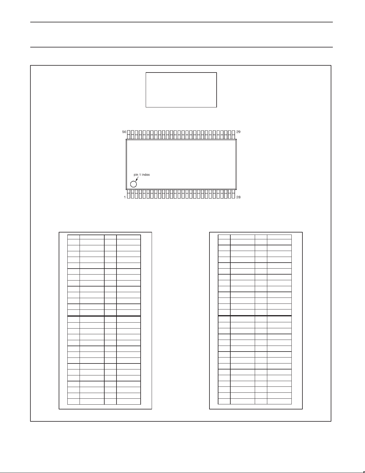
28L202
Pin Configurations
80xxx
56 Pin TSSOP
Pin Function Pin Function
1 Vcc 29 CEN
2 Vss 30 WRN
3 A6 31 RDN
4 A5 32 TxDB
5 A4 33 I/O7B
6 A3 34 I/O6B
7 RxDA 35 I/O5B
8 RESET 36 I/O4B
9 D7 37 I/O3B
10 D6 38 I/O2B
11 D5 39 I/O1B
12 D4 40 I/O0B
13 Vcc 41 Vcc
14 NC 42 Vcc
15 Vss 43 Vss
16 Vss 44 Vss
17 D3 45 I/O7A
18 D2 46 I/O6A
19 D1 47 I/O5A
20 D0 48 I/O4A
21 I / M 49 I/O3A
22 RxDB 50 I/O2A
23 A2 51 I/O1A
24 A1 52 I/O0A
25 A0 53 TxDA
26 (IACKN) 54 IRQN
27 Vcc 55
X1 / SCLK
28 Vss 56 X2
68xxx
56 Pin TSSOP
Pin Function Pin Function
1 Vcc 29 CEN
2 Vss 30 RWN
3 A6 31 DACKN
4 A5 32 TxDB
5 A4 33 I/O7B
6 A3 34 I/O6B
7 RxDA 35 I/O5B
8 RESETN 36 I/O4B
9 D7 37 I/O3B
10 D6 38 I/O2B
11 D5 39 I/O1B
12 D4 40 I/O0B
13 Vcc 41 Vcc
14 NC 42 Vcc
15 Vss 43 Vss
16 Vss 44 Vss
17 D3 45 I/O7A
18 D2 46 I/O6A
19 D1 47 I/O5A
20 D0 48 I/O4A
21 I / M 49 I/O3A
22 RxDB 50 I/O2A
23 A2 51 I/O1A
24 A1 52 I/O0A
25 A0 53 TxDA
26 IACKN 54 IRQN
27 Vcc 55
X1 / SCLK
28 Vss 56 X2
2000 Feb 10
SD00691
5

Philips Semiconductors Objective specification
SC28L202Dual UART
28L202
Pin Configuration
50 49 48 47 46 45 44 43 4252 41 40
51
1
2
3
4
5
6
7
8
9
10
11
12
13
15 16 17 18 19 20 21 22 23 2414 25 26
52 Pin
PQFP
39
38
37
36
35
34
33
32
31
30
29
28
27
80xxx
52 Pin PQFP
Pin Function Pin Function
1 RxDA 27 I/O5B
2 RESET 28 I/O4B
3 D7 29 I/O3B
4 D6 30 I/O2B
5 D5 31 I/O1B
6 D4 32 I/O0B
7 Vcc 33 Vcc
8 Vss 34 Vss
9 D3 35 I/O7A
10 D2 36 I/O6A
11 D1 37 I/O5A
12 D0 38 I/O4A
13 I / M 39 I/O3A
14 RxDB 40 I/O2A
15 A2 41 I/O1A
16 A1 42 I/O0A
17 A0 43 TxDA
18 (IACKN) 44 IRQN
19 Vcc 45
X1 / SCLK
20 Vss 46 X2
21 CEN 47 Vcc
22 WRN 48 Vss
23 RDN 49 A6
24 TxDB 50 A5
25 I/O7B 51 A4
26 I/O6B 52 A3
68xxx
52 Pin PQFP
Pin Function Pin Function
1 RxDA 27 I/O5B
2 RESETN 28 I/O4B
3 D7 29 I/O3B
4 D6 30 I/O2B
5 D5 31 I/O1B
6 D4 32 I/O0B
7 Vcc 33 Vcc
8 Vss 34 Vss
9 D3 35 I/O7A
10 D2 36 I/O6A
11 D1 37 I/O5A
12 D0 38 I/O4A
13 I / M 39 I/O3A
14 RxDB 40 I/O2A
15 A2 41 I/O1A
16 A1 42 I/O0A
17 A0 43 TxDA
18 IACKN 44 IRQN
19 Vcc 45
X1 / SCLK
20 Vss 46 X2
21 CEN 47 Vcc
22 RWN 48 Vss
23 DACKN 49 A6
24 TxDB 50 A5
25 I/O7B 51 A4
26 I/O6B 52 A3
2000 Feb 10
SD00692
6

Philips Semiconductors Objective specification
SC28L202Dual UART
OVERALL DESCRIPTION
The SC28L202 is composed of several functional blocks. They are
listed in the approximate order of hierarchy as seen from the pins of
the device.
•Bus interface. 68K or x86 format
•Timing Circuits
•I/O Ports
•UARTs
•Transmitters and Receivers
•FIFO Structures
•Arbitrating Interrupt Structure
•Character & Address Recognition
•Flow Control
•Test and Software compatibility with previous Philips (Signetics)
UARTs
BRIEF DESCRIPTION OF FUNCTIONAL BLOCKS
Bus Interface
The Two basic modes of Bus Interface
The bus interface operates in “68K” or “x86” format as selected by
the I/M pin. The signals used by this section are the Address, Data
bus, Chip select, read/write, Data acknowledge and Interrupt
acknowledge and Interrupt request. Assertion of DACKN requires
two edges of the Sclk after the assertion of CEN. The default mode
is the x86 mode. Pin or register programming may change it to he
68K mode
Timing Circuits
Crystal Oscillator
The crystal oscillator is the main timing element for the 28L202. It is
nominally set at 14.7456 MHz. Operation with a crystal as a
frequency standard is specified from 7 MHz to 16.2 MHz The use of
an external clock allows all frequencies to 50 MHz. Clock prescalers
are provided to match various available system clocks to those
needed for baud rate generation.
NOTE: if an external clock is used X2 should not drive more
than 2 CMOS or 2 TTL equivalents.
Fixed Rate BRG
The BRG is the baud rate generator, is driven by the X1/Sclk input
through a programmable prescale divider. It generates all of the 27
“fixed” internal baud rates. This baud rate generator is designed to
generate the industry standard baud rates from a 14.7456 MHz
crystal or clock frequency. X1/Sclk frequencies different from
14.7456 MHz will cause the “fixed” baud rates to change by exactly
the ratio of 14.7456 to the different frequency.
Counter–Timer
The two counter–timers are programmable 16 bit “down” counters. It
provides miscellaneous baud rates, timing periods and acts as an
extra watchdog timer for the receivers. It has 8 programmable clock
sources derived from internal and external signals. It may also act
as a character counter for the receiver. Interrupts from the counter
timer are generated as it passes through zero.
Programmable BRG (PBRG)
This is another 16 bit programmable counter to generate only baud
rates or miscellaneous clock frequencies. Its output is available to
the receivers and transmitters and may be delivered to I/O ports. It
has 8 programmable clock sources derived from internal and
external signals.
I/O ports
The SC28L202 is provided with 16 I/O ports. These ports are true
input and/or output structures and are equipped with a change of
state detector. The input circuit of these pins is always active. Under
program control the ports my display internal signals or static logic
levels. The functions represented by the I/O ports include hardware
flow control. Modem signals, signals for interrupt conditions or
various internal clocks and timing intervals. Noisy inputs to the I/O
ports are filtered (de–bounced) by a 38.4 KHz clock. Change of
state detectors are provided for each pin and are always available.
UARTs
The UARTs are fully independent, full duplex and provide all normal
asynchronous functions: 5 to 8 data bits, parity odd or even,
programmable stop bit length, false start bit detection. Also provided
are 256 byte FIFOs Xon/Xoff software flow. The BRG,
Counter–timer , or external clocks provide the baud rates. The
receivers and transmitters may operate in either the “1x” or “16x”
modes.
The control section recognizes two address schemes. One is the
subset of the other: a four (4) bit and an eight (7) bit address
spaces. The purpose of this is to provide a large degree of software
compatibility with previous Philips/Signetics UARTs.
Transmitters and Receivers
The transmitters and receivers are independent devices capable of
full duplex operation. Baud rates, interrupt and status conditions are
under separate control. Transmitters have automatic simplex
“turnaround”. Receivers have RTS and Xon/Xoff flow control and a
three character recognition system.
FIFO Structures
The FIFO structure is 256 bytes for each of the four FIFOs in the
DUART. They are organized as 11 bit words for the receiver and 8
bye words for the transmitter. The interrupt level may be set at any
value from 0 to 255. The interrupt level is independently set for each
FIFO.
FIFO interrupt and DMA fill/empty levels are controlled by the RxFIL
and TxFIL registers which may set any level of the from 0 to 255.
The signals associated with the FIFO fill levels are available to the
I/O pins (for interrupt or DMA) and to the arbitrating interrupt system
for “fine tuning” of the arbitration authority.
Intelligent Interrupt Arbitration
The interrupt system uses a highly programmable arbitrating
technique to establish when an interrupt should be presented to the
processor. The advantageous feature of this system is the
presentation of the context of the interrupt. It is presented in both a
current interrupt register and in the interrupt vector. The context of
the interrupt shows the interrupting channel, identifies which of the
18 possible sources in requesting interrupt service and in the case
of a receiver or transmitter gives the current fill level of the FIFO.
The content of the current interrupt register also drives the Global
Registers of the interrupt system. These registers are indirect
addresses (pointers) to the interrupt source requesting service.
Programming of Bid Control Registers allows the interrupt level of
any source to be varied at any time over a range of 256 levels.
Character and Address Recognition
The character recognition system is designed as a general–purpose
system. There is one for each UART. Each recognition block stores
2000 Feb 10
7

Philips Semiconductors Objective specification
SC28L202Dual UART
up to three characters. The recognition is done on a byte boundary
and sets status and interrupt when recognition events occur. Three
modes of automatic operation are provided for the in–band flow
control and three modes of automatic operation are provided for
address recognition. Both in–band flow control and address
recognition may also be completely under the control of the host
processor.
A subset of the recognition system is Xon/Xoff character recognition
and the recognition of the multi–drop address character. If Xon/Xoff
or multi–dorp function is enabled the recognition system passes the
information about the recognition event to the appropriate receiver
or transmitter state machine for execution. In any case the
information about a recognition event is available to the interrupt
system and to the control processor.
Flow Control
Flow control is implemented in either the traditional RTS/CTS
protocol or in the “inbound” Xon/Xoff method. Both may be
controlled by fully/partially automatic methods or by interrupt
generation.
Test Modes and Software
Four test modes are provided to verify UART function and processor
interface integrity. The first three are Auto echo, Local Loop Back,
and Remote Loop Back. Through local loop back the software
developer may verify all of the interrupt, flow control; the hardware
designer verify all of the timing and pin connections. This information
is obtained without any recourse to external test equipment, logic
analyzers or terminals.
The fourth, Receiver Error Loop back verification, employs a method
of automatic checking (accounting for transmission delays) of the
transmitted data to as echoed back through the remote receiver.
Errors generate interrupt and status events.
DET AILED DESCRIPTIONS
NOTE: For the convenience of the reader some paragraphs
of the following sections are repeated in descriptions of
closely linked functions described in other sections.
Bus Interface
The bus interface operates in two modes selected by the I/M pin. If
this pin is high or left open the signals DACKN signal is not
generated or used and data flow to and from the chip is controlled
by the state the CEN, RDN, WRN pin combination. If the I/M pin is
tied low the data is written to the device when the DACKN pin is
asserted low by the DUART. Read data is presented by a delay from
CEN active.
The Host interface is comprised of the signal pins CEN, WRN RDN,
(or R/WN) IACKN, DACKN, IRQN, 6 address pins and 8 three–state
data bus pins. Addressing of the various functions of the DUART is
through the address bus A(6:0). Data is presented on the 8–bit data
bus.
DACKN Cycle
When operating in the “68K” mode bus cycle completion is indicated
by the DACKN pin (an open drain signal) going low. The timing of
DACKN is by GCCR(6) where two time delays area available. The
delay begins with the falling edge of CEN and DACKN is presented
after either two edges of he X1/Sclk (1/2 X1/Sclk Cycle) or, under
program control, a short internal delay of less than 50 ns. Usually in
this mode the address and data are set up with respect to the
leading edges of the bus cycle.
The DACKN pin is a three state driver. At the termination of an
access to the L202 a very short pulse (less than 5 ns) drives the pin
high and immediately returns to the high impedance state. This will
occur at the termination of the CEN or IACKN cycle.
NOTE: The faster X86 timing may be used in the 68K mode IF the
bus cycles are faster than 1/2 period of the Sclk clock. Withdrawing
CEN before DACKN prevents the generation of DACKN. In this case
bus timing is effectively that of the X86 mode.
When operating in the “x86” mode DACKN is not generated. Data is
written on the termination of CEN or WRN whichever one occurs
first. Read data is presented from the leading edge of the read
condition (CEN and RDN both low).
IACKN Cycle, Update CIR
When the host CPU responds to the interrupt, it will usually assert
the IACKN signal low. This will cause the intelligent interrupt system
of the DUART to generate an IACKN cycle in which the condition of
the interrupting source is determined. When IACKN asserts, the last
valid of the interrupt arbitration cycle is captured in the CIR. The
value captured presents all of the important details of the highest
priority interrupt at the moment the IACKN (or the ”Update CIR”
command) was asserted. Due to system interrupt latency the
interrupt condition captured by the CIR may not be the condition that
caused the initial assertion of the interrupt.
The Dual UART will respond to the IACKN cycle with an interrupt
vector. The interrupt vector may be a fixed value, the content of the
Interrupt Vector Register, or when ”Interrupt Vector Modification” is
enabled via ICR, it may contain codes for the interrupt type and/or
interrupting channel. This allows the interrupt vector to steer the
interrupt service directly to the proper service routine. The interrupt
value captured in the CIR remains until another IACKN or “Update
CIR” command is given to the DUART. The interrupting channel and
interrupt type fields of the CIR set the current ”interrupt context” of
the DUART. The channel component of the interrupt context allows
the use of Global Interrupt Information registers that appear at fixed
positions in the register address map. For example, a read of the
Global RxFIFO will read the channel B RxFIFO if the CIR interrupt
context is channel B receiver. At another time read of the GRxFIFO
may read the channel A RxFIFO (CIR holds a channel A receiver
interrupt) and so on. Global registers exist to facilitate qualifying the
interrupt parameters and for writing to and reading from FIFOs
without explicitly addressing them.
The CIR will load with 0x00 if IACKN or Update CIR is asserted
when the arbitration circuit is NOT asserting an interrupt. In this
condition there is no arbitration value that exceeds the threshold
value. When Interrupt vector modification is active in this situation
the interrupt vector bits associated with the CIR will all be zero. A
zero type field indicates nothing with in the DUART is requiring
processor service.
NOTE: IACKN is essentially a special read action where the value of
the interrupt vector is presented to the data bus.
Timing Circuit
Crystal Oscillator
The crystal oscillator operates directly from a crystal, tuned between
7.0 MHz and 16.2 MHz connected across the X1/Sclk and X2 inputs
with a minimum of external components. BRG values listed for the
clock select registers correspond to a 14.7456 MHz crystal
frequency. Use of different frequencies will change the “standard”
baud rates by precisely the ratio of 14.7456 MHz to the different
crystal frequency.
An external clock up to 50 MHz frequency range may be connected
to X1/Sclk pin. If an external clock is used instead of a crystal,
X1/Sclk must be driven and X2 left floating or driving a load of not
2000 Feb 10
8

Philips Semiconductors Objective specification
SC28L202Dual UART
more than 2 CMOS or TTL equivalents. The X1/Sclk clock serves as
the basic timing reference for the baud rate generator (BRG) and is
available to the programmable BRG (PBRG), counter–timers,
control logic and the UART receivers and transmitters.
Baud Rate Generator BRG
The baud rate generator operates from the oscillator or external
X1/Sclk clock input and generates 27 commonly used data
communications baud rates (including MIDDI) ranging from 50 to
921.6K baud. These common rates may be increased (up to 3000K
baud) when faster clocks are used on the X1/Sclk clock input. (See
Receiver and Transmitter Clock Select Register descriptions.) All of
these are available simultaneously for use by any receiver or
transmitter. The clock outputs from the BRG are at 16X the actual
baud rate.
Please see counter timer description for a description of the
frequency error that the asynchronous protocol may tolerate.
Depending on character length it varies from 4.1% to 6.7%.
Counter–Timer
The two Counter/Timers are programmable 16 bit dividers that are
used for generating miscellaneous clocks or generating timeout
periods. These clocks may be used by any or all of the receivers
and transmitters in the DUART or may be directed to an I/O pin for
miscellaneous use.
Counter/Timer programming
The counter timer is a 16–bit programmable divider that operates in
one of four modes: character count, counter, timer, and time out.
Character count counts characters. The timer mode generates a
square wave. In the counter mode it generates a time delay. In the
time out mode it monitors the time between received characters.
The C/T uses the numbers loaded into the Counter/Timer Lower
Register (CTPL) and the Counter/Timer Upper Register (CTPU) as
its divisor. The counter timer is controlled with six commands:
Start/Stop C/T, Read/Write Counter/Timer lower register and
Read/Write Counter/Timer upper register. These commands have
slight differences depending on the mode of operation. Please see
the detail of the commands under the CTPL/CTPU Register
descriptions.
Whenever the these timers are selected via the receiver or
transmitter Clock Select register their output will be configured as a
16x clock for the respective receiver or transmitter. Therefore one
needs to program the timers to generate a clock 16 times faster than
the data rate. The formula for calculating ’n’, the number loaded to
the CTPU and CTPL registers, based on a particular input clock
frequency is shown below.
For the timer mode the formula is as follows:
n +
NOTE: ‘n’ may assume a value of 1. In previous Philips data
communications controllers this value was not allowed. The
Counter/Timer Clock Select Register (CTCS) controls the
Counter/Timer input frequency.
The frequency generated from the above formula will be at a rate 16
times faster than the desired baud rate. The transmitter and receiver
state machines include divide by 16 circuits, which provide the final
frequency and provide various timing edges used in the qualifying
the serial data bit stream. Often this division will result in a
non–integer value: 26.3 for example. One may only program integer
numbers to a digital divider. There for 26 would be chosen. If 26.7
were the result of the division then 27 would be chosen. This gives a
baud rate error of 0.3/26.3 or 0.3/26.7 that yields a percentage error
Clockinputfrequency
(2 16 (Baud rate desired))
of 1.14% or 1.12% respectively, well within the ability of the
asynchronous mode of operation. Higher input frequency to the
counter reduces the error effect of the fractional division
One should be cautious about the assumed benign effects of small
errors since the other receiver or transmitter with which one is
communicating may also have a small error in the precise baud rate.
In a ”clean” communications environment using one start bit, eight
data bits and one stop bit the total difference allowed between the
transmitter and receiver frequency is approximately 4.6%. Less than
eight data bits will increase this percentage.
Programmable Baud Rate Generators. PBRG
Two PBRG Counters (Used only for random baud rate generation)
The two PBRG Timers are programmable 16 bit dividers that are
used for generating miscellaneous clocks. These clocks may be
used by any or all of the receivers and transmitters in the SC28L202
or output to the general purpose I/O pins.
Each timer unit has eight different clock sources available to it as
described in the PBRG clock source Register. Note that the timer
run and stop controls are also contained in this register. The PBRG
counters generate a symmetrical square wave whose half period is
equal in time to the division of the selected PBRG Timer clock
source by the number loaded to the PBRGPU and PBRGPL Preset
Registers. Thus, the output frequency will be the clock source
frequency divided by twice the 16 bit value loaded to these registers.
This is the result of counting down once for the high portion of the
output wave and once for the low portion.
Whenever the these timers are selected via the receiver or
transmitter Clock Select register their output will be configured as a
16x clock for the respective receiver or transmitter. Therefore one
needs to program the timers to generate a clock 16 times faster than
the data rate. The formula for calculating ’n’, the number loaded to
the PBRGPL and PBRGPU registers, is the same as shown above
I/O Ports
Eight I/O ports are “loosely” provided for each channel. They may be
programmed to be inputs or outputs. The input circuits are always
active whether programmed as and input or an output. In general a
2–bit code in the
function these pins will present. All I/O ports default to high
impedance input state on power up.
When calling software written for previous Philips (Signetics)
DUARTs the user should be sure to declare I/O ports to be
inputs where drivers may be attached to an I/O port pin that
previous software had expected to be an output.
Input Characteristics of the I/O ports
Eight I/O pins are provided for each channel. These pins are
configured individually to be inputs or outputs. As inputs they may
be used to bring external data to the bus, as clocks for internal
functions or external control signals. Each I/O pin has a ”Change of
State” detector. The change detectors are used to signal a change in
the signal level at the pin (Either 0 to 1 or 1 to 0 transitions). The
level change on these pins must be stable for 25 to 50 us (two
edges of the 38.4 KHz baud rate clock) before the detectors will
signal a valid change. These are typically used for interface signals
from modems to the DUART and from there to the host.
Output Port of the I/O ports
The OPR, I/OPCR, MR, and CR registers may control the I/O pins
when configured as outputs. (For the control in the loser 16 position
address space the control register is the OPCR) Via appropriate
programming the pins of the output port may be configures as
another parallel port to external circuits, or they may represent
internal conditions of the UART. When this 8–bit port is used as a
I/OPCR
(I/O Port Control Register) controls what
2000 Feb 10
9

Philips Semiconductors Objective specification
SC28L202Dual UART
general–purpose output port, the output port pins drive inverse logic
levels of the individual bits in the Output Port Register (OPR). The
OPR register is set and reset by writing to the SOPR and ROPR
addresses. (See the description of the SOPR and ROPR registers).
The output pins will drive the same data polarity of the OPR
registers. The I/OPCR (or the OPCR) register conditions these
output pins to be controlled by the OPR or by other signals in the
chip. Output ports are driven high on hardware reset.
UART Operation
Receiver and Transmitter
The Dual UART has two full duplex asynchronous
receiver/transmitters. The operating frequency for the receiver and
transmitter can be selected independently from the baud rate
generator, the counter, or from an external input. Registers that are
central to basic full–duplex operation are the mode registers (MR0,
MR1 and MR2), the clock select registers (RxCSR and TxCSR), the
command register (CR), the status register (SR), the transmit
holding register (TxFIFO), the receive holding register (RxFIFO),
interrupt status register (ISR) and interrupt mask register (IMR).
MR3 does not exist in 92 mode. MR3 is used in the control of the
intelligent operations of the L202.
Transmitter Status Bits
The SR (Status Register, one per UART) contains two bits that show
the condition of the transmitter FIFO. These bits are TxRDY and Tx
Idle. TxRDY means the TxFIFO has space available for one or more
bytes; Tx Idle means The TxFIFO is completely empty and the last
stop bit has been completed – the transmitter is underrun. Tx Idle
can not be active without TxRDY also being active. These two bits
will go active upon initial enabling of the transmitter
Transmission resumes and the Tx Idle bit is cleared when the CPU
loads at least one new character into the TxFIFO. The TxRDY will
not extinguish until the TxFIFO is completely full. The TxRDY bit will
always be active when the transmitter is enabled and there is at
lease one open position in the TxFIFO.
The transmitter is disabled by a hardware reset, a transmitter reset
in the command register or by the transmitter disable bit also in the
command register (CR). The transmitter must be explicitly enabled
via the CR before transmission can begin. Note that characters
cannot be loaded into the TxFIFO while the transmitter is disabled,
hence it is necessary to enable the transmitter and then load the
TxFIFO. It is not possible to load the TxFIFO and then enable the
transmission.
Note the difference between transmitter disable and transmitter
reset.
Either hardware or software may cause the reset action. When reset
the transmitter stops transmission immediately. The transmit data
output will be driven high, transmitter status bits set to zero and any
data remaining in the TxFIFO is effectively discarded.
The transmitter disable is controlled by the Tx Enable bit in the
command register. Setting this bit to zero will not stop the transmitter
immediately but will allow it to complete any tasks presently
underway. It is only when the last character in the TxFIFO and its
stop bit(s) have been transmitted that the transmitter will go to its
disabled state. While the transmitter enable/disable bit in the
command register is at zero the TxFIFO will not accept any more
characters and the Tx Idle and TxRDY bits of the status register set
to zero.
Transmission of ”break”
Transmission of a break character is often needed as a
synchronizing condition in a data stream. The ”break” is defined as a
start bit followed by all zero data bits by a zero parity bit (if parity is
enabled) and a zero in the stop bit position. The forgoing is the
minimum time to define a break. The transmitter can be forced to
send a break (continuous low condition) by issuing a start break
command via the CR. Once the break starts, the TxD output
remains low until the host issues a command to ”stop break” via the
CR or the transmitter is issued a software or hardware reset. In
normal operation the break is usually much longer than one
character time.
1x and 16x modes, Transmitter
The transmitter clocking has two modes: 16x and 1x. Data is always
sent at the 1x rate. However the logic of the transmitter may be
operated with a clock that is 16 times faster than the data rate or at
the same rate as the data i.e. 1x. All clocks selected internally for
the transmitter (and the receiver) will be 16x clocks. Only when an
external clock is selected may the transmitter logic and state
machine operate in the 1x mode. The 1x or 16x clocking makes little
difference in transmitter operation. (This is not true in the receiver)
In the 16X–clock mode the transmitter will recognize a byte in the
TxFIFO within 1/16 to 2/16–bit time and thus begin transmission of
the start bit. In the 1x mode this delay may be up to 2 bit times.
Transmitter FIFO
The FIFO configuration of the as 28L202 is 256 8–bit words.
Interrupt levels may be set to any level within the FIFO size and may
be set differently for each FIFO. Logic associated with the FIFO
encodes the number of empty positions for presentation to the
interrupt arbitration system. The encoding value is the number of
empty positions. Thus, an empty TxFIFO will bid with the value or
255; when full it will not bid at all; one position empty bids with the
value 0. A Full TxFIFO will not bid since no character is available.
Normally TxFIFO will present a bid to the arbitration system
whenever it has one or more empty positions. The Bits of the
TxFIFO Interrupt Level in the MR0(5:4) allow the user to modify this
characteristic so that bidding will not start until one of four levels
(one or more filled, empty, 16 filled, 240 filled, full) have been
reached. As will be shown later this feature may be used to make
moderate improvements in the interrupt service efficiency . A similar
system exists for the Receiver.
Transmitter
The 28L202 is conditioned to transmit data when the transmitter is
enabled through the command register. The transmitter of the
28L202 indicates to the CPU that it is ready to accept a character by
setting the ISR TxRDY bit in the status register. This condition can
be programmed to generate an interrupt request at
When the transmitter is initially enabled the TxRDY and Tx Idle bits
will be set in the status register. When a character is loaded to the
transmit FIFO the Tx Idle bit will be reset. The Tx Idle bit will not set
until the transmit FIFO is empty and the transmit shift register has
finished transmitting the stop bit of the last character written to the
transmit FIFO.
The TxRDY bit is set whenever the transmitter is enabled and the
TxFIFO is not full. Data is transferred from the holding register to
transmit shift register when it is idle or has completed transmission
of the previous character. Characters cannot be loaded into the
TxFIFO while the transmitter is disabled.
The transmitter converts the parallel data from the CPU to a serial
bit stream on the TxD output pin. It automatically sends a start bit
I/O4
or IRQN.
2000 Feb 10
10

Philips Semiconductors Objective specification
SC28L202Dual UART
followed by the programmed number of data bits, an optional parity
bit, and the programmed number of stop bits. The least significant
bit is sent first. Following the transmission of the stop bits, if a new
character is not available in the TxFIFO, the TxD output remains
High and the Tx Idle bit in the Status Register (SR) will be set to 1.
Transmission resumes and the Tx Idle bit is cleared when the CPU
loads a new character into the TxFIFO.
If the transmitter is disabled, it continues operating until the
character currently being transmitted is completely sent out. The
transmitter can be forced to send a continuous Low condition by
issuing a send break command. The transmitter can be reset
through a software command. If it is reset, operation ceases
immediately and the transmitter must be enabled through the
command register before resuming operation.
If CTS option of hardware flow control is enabled (MR2 [4] = 1), the
CTS input at I/O0 or I/O1 must be Low in order for the character to
be transmitted. The transmitter will check the state of the CTS input
at the beginning of each character transmitted. If it is found to be
High, the transmitter will delay the transmission of any following
characters until the CTS has returned to the low state. CTS going
high during the serialization of a character will not affect that
character.
It is an interesting point of the I/O system inputs being always active
that by enabling transmitter to be sensitive the I/O0 or I/O1 and then
controlling the I/O pin as an out put that one is able to control the
transmitter flow via software control of the I/O pin.
The transmitter can also control the RTSN outputs, I/O0 or I/O1 via
MR2 [5]. When this mode of operation is set (often referred to as the
RS–485 method) the meaning of the I/O0 B or I/O1 B signals is “all
bytes loaded to the transmitter’s FIFO have been transmitted
including the last stop bit(s). See the MR2(5) description for enabling
this automatic function.
Receiver Operation
Receiver
The receiver accepts serial data on the RxD pin, converts the serial
input to parallel format, checks for start bit, stop bit, parity bit (if any),
framing error or break condition, and presents the assembled
character and its status condition to the CPU via the RxFIFO. Three
status bits are FIFOed with each character received. The RxFIFO is
really 11 bits wide: eight data and 3 status. Unused FIFO bits for
character lengths less than 8 bits are set to zero.
It is important to note that in the asynchronous protocol the receiver
logic considers the entire message to be contained within the start
bit to the stop bit. It is not aware that a message may contain many
characters. The receiver returns to its idle mode at the end of each
stop bit! As described below it immediately begins to search for
another start bit, which is normally, of course, immediately
forthcoming.
1x and 16x mode, Receiver
The receiver operates in one of two modes: 1x and 16x. Of the two,
the 16x is more robust and the preferred mode. Although the 1x
mode may allow a faster data rate is does not provide for the
alignment of the receiver 1x data clock to that of the transmitter. This
strongly implies that the 1x clock of the remote transmitter is
available to the receiver; the two devices are physically close to
each other.
The 16x mode operates the receiver logic at a rate 16 times faster
than the 1x data rate. This allows for validation of the start bit length,
the validation of level changes at the receiver serial data input
(RxD), and the validation of the stop bit length. Of most importance
in the 16x mode is the ability of the receiver logic to align the phase
of the internally generated receiver 1x data clock to that of the
received start bit of the remote transmitter. This occurs with an
accuracy of less than 1/16 bit time.
Receiver
The receiver of the 28L202 is conditioned to receive data when
enabled through the command register. The receiver looks for a
High–to–Low (mark–to–space) transition of the start bit on the RxD
input pin. If a transition is detected, the state of the RxD pin is
sampled each 16X clock for 7–1/2 clock periods (16X clock mode)
or at the next rising edge of the bit time clock (1X clock mode). If
RxD is sampled high, (that is the start bit was low less than 7/16 to
½ bit time) the start bit is judged invalid and the search for another
valid start bit begins immediately. If RxD is still low, a valid start bit is
assumed and the receiver then continues to sample the input at
one–bit time intervals at the theoretical center of the bit. When the
proper number of data bits and parity bit (if used) have been
assembled, and one half–stop bit has been detected the receiver
loads the byte to the FIFO. The least significant bit is received first.
The data is then transferred to the Receive FIFO and the ISR
RxRDY bit in the SR is set to a 1. This condition can be
programmed to generate an interrupt at IRQN or I/O[4:5] for
channels A or B respectively. If the character length is less than 8
bits, the most significant unused bits in the RxFIFO are set to zero.
After the stop bit is detected, the receiver will immediately look for
the next start bit. However, if a non–zero character was received
with the stop bit at a zero level (framing error) and RxD remains Low
for at least another one half bit time after the stop bit was sampled,
then the receiver operates as if a new start bit had been detected. It
then continues assembling the next character.
The error conditions of parity error, framing error, and overrun error
(if any) are written to the SR at the received character boundary.
This is just before the RxRDY status bit is set.
A break condition is detected when RxD is Low for the entire
character including the parity bit, if used, and stop bit. When a break
is found a character consisting of all zeros will be loaded into the
RxFIFO, the received break bit in the SR and the “change of break”
bit in the ISR are set to 1 and the receiver ready is set in the SR.
The RxD input must
RxC1x clock for the receiver to recognize the end of the break
condition. At the end of the break condition the search for the next
start bit begins.
Two edges of the RxC1x clock will usually require a high time of one
RxC1x clock period or 3 RxC1x edges since the clock of the
controller is usually not synchronous to nor in phase with the RxC1x
clock.
Receiver Status Bits
There are five (5) status bits that are evaluated with each byte (or
character) received: received break, framing error, parity error,
overrun error, and change of break. The first three are appended to
each byte and stored in the RxFIFO. The last two are not
necessarily related to the byte being received or a byte that is in the
RxFIFO. They are however developed by the receiver state
machine.
The ”received break” will always be associated with a zero byte in
the RxFIFO. It means that zero character was a break character and
not a zero data byte. The reception of a break condition will always
set the ”change of break” (see below) status bit in the Interrupt
Status Register (ISR).
return to high for two (2) clock edges
of the
2000 Feb 10
11

Philips Semiconductors Objective specification
SC28L202Dual UART
The Change of break condition is reset by a reset error status
command in the command register
A framing error occurs when a non–zero character was seen and
that character has a zero in the stop bit position.
The parity error indicates that the receiver–generated parity was not
the same as that sent by the transmitter.
The framing, parity and received break status bits are reset when
the associated data byte is read from the RxFIFO since these “error”
conditions are attached to the byte that has the error
The overrun error occurs when the RxFIFO is full, the receiver shift
register is full, and another start bit is detected. At this moment the
receiver has 257 valid characters and the start bit of the 258
th
has
been seen. At this point the host has approximately 6/16 bit time to
read a byte from the RxFIFO or the overrun condition will be set.
th
The 258
character then overruns the 257th and the 258th the 259
and so on until an open position in the RxFIFO is seen. (“seen”
meaning at least one byte was read from the RxFIFO.)
Overrun is cleared by a use of the “error reset” command in the
command register.
The fundamental meaning of the overrun is that data has been lost.
Data in the RxFIFO remains valid. The receiver will begin placing
characters in the RxFIFO as soon as a position becomes vacant.
NOTE: Precaution must be taken when reading an overrun FIFO.
There will be 256
th
valid characters in the receiver FIFO. There will
be one character in the receiver shift register. However it will NOT
be known if more than one “over–running” character has been
received since the overrun bit was set. The 257
and read as valid but it will not be known how many characters were
lost between the two characters of the 256
th
character received
th
and 257th reads of the
RxFIFO. In the 8-bit mode, the numbers 8 and 9 replace the
numbers 256 and 257 above.
The ”Change of break” means that either a break has been detected
or that the break condition has been cleared. This bit is available in
the ISR. The break change bit being set in the ISR and the received
break bit being set in the SR will signal the beginning of a break. At
the termination of the break condition only the change of break in
the ISR will be set. After the break condition is detected the
termination of the break will only be recognized when the RxD input
has returned to the high state for two successive edges of the 1x
clock; 1/2 to 1 bit time. (see above)
The receiver is disabled by reset or via CR commands. A disabled
receiver will not interrupt the host CPU under any circumstance in
the normal mode of operation. If the receiver is in the multi–drop or
special mode, it will be partially enabled and thus may cause an
interrupt. Refer to section on Wake–Up and the register description
for MR1 for more information.
Receiver FIFO
The receiver buffer memory is a 256 byte FIFO with three status bits
appended to each data byte. (The FIFO is then 256 11–bit ”words”).
The receiver state machine gathers the bits from the receiver shift
register and the status bits from the receiver logic and writes the
assembled byte and status bits to the RxFIFO shortly after the stop
bit has been sampled. Logic associated with the FIFO encodes the
number of filled positions for presentation to the interrupt arbitration
system. The encoding is always the number of filled positions. Thus,
a full RxFIFO will bid with the value of 255 and the Status Register
RxFULL bit is set. When empty it will not bit at all. One position
occupied bids with the value 1. An empty FIFO will not bid since no
character is available.
Normally RxFIFO will present a bid to the arbitration system
whenever it has one or more filled positions. The bits of the RxFIFO
Interrupt Offset Level (RxFIL) or the bits of the MR2(3:2) allow the
user to modify this characteristic so that bidding will not start until
one of four levels (one or more filled, 64 filled, 192 filled, full) have
been reached. As will be shown later this feature may be used to
make slight improvements in the interrupt service efficiency . A
similar system exists in the transmitter.
RxFIFO Status Bits. Status reporting modes
This description applies to the upper three bits in the ”Status
Register” These three bits are not ”in the status register”; they are
part of the RxFIFO. The three status bits at the output of the RxFIFO
are presented as the upper three bits of the status register included
in each UART.
The error status of a character, as reported by a read of the SR
th
(status register upper three bits) can be provided in two ways, as
programmed by the error mode control bit in the mode register:
”Character mode ” or the ”Block Mode”. The block mode may be
further modified (via a CR command) to set the status bits as the
characters enter the FIFO or as they are read from the FIFO.
In the ’character’ mode, status is provided on a character by
character basis as the characters are read from the RxFIFO: the
”status” applies only to the character at the output of the RxFIFO –
The next character to be read.
In the ’block’ mode (on entry) the status provided in the SR for these
three bits is the logical OR of the status for all characters coming to
the input of the RxFIFO since the last reset error command was
issued. In this mode each of the status bits stored in the RxFIFO are
passed through a latch as they are sequentially written to the
receiver FIFO. If any of the characters has an error bit set that latch
will set and remain set until it is reset with a “receiver reset” issued
from the command register or a chip reset is issued. The purpose of
this mode is indicating an error in the data block as opposed to an
error in a character. This mode improves receiver service efficiency.
In modern systems with low error rates, it is more efficient to ask for
retransmit of a block error data than to analyze it on a byte by byte
system.
The above paragraph describes the block mode activity as the data
is entered to the RxFIFO. Normally the status would be read only
once – at the beginning of the service to the receiver interrupt. If an
error is not set then the entire amount of data in the RxFIFO would
be read without any more reading if the receiver status. This
effectively doubles the efficiency of reading the receiver RxFIFO.
The use of the block mode on Exit passes the data and error
conditions as the RxFIFO is read. Here the final read of the status
register would be after the last byte was read from the RxFIFO. This
delays the knowledge of an error condition until after the data has
been read.
The latch used in the block mode to indicate ”problem data” is
usually set as the characters are read out of the RxFIFO. Via a
command in the CR the latch may be configured to set as error
characters are loaded to the RxFIFO. This gives the advantage of
indicating ”problem data” up to 256 (or the FIFO size) characters
earlier.
In either mode, reading the SR does not affect the RxFIFO. The
RxFIFO address is advanced only when the RxFIFO is read.
Therefore, the SR should be read prior to reading the corresponding
data character.
2000 Feb 10
12

Philips Semiconductors Objective specification
SC28L202Dual UART
If the RxFIFO is full when a new character is received, the character is held in the receiver shift register until a position is available in the RxFIFO. At this time there are 257 valid characters in the RxFIFO. If an additional character is received while this state exists, the contents of the RxFIFO are not affected: the character previously in the shift register is lost and the overrun error status bit, SR [4], will be set upon receipt of the start bit of the new (overrunning) character. Wake Up Mode (Also the “9–bit”, “multi–drop”, “party; line” or Special mode) The SC28L202 provides four modes of this common asynchronous ”party line” protocol where the parity bit is used to indicate that a byte is address data or information data. Three automatic modes and the default Host operated mode are provided. The automatic mode has several sub modes (see below). In the full automatic the internal state machine devoted to this function will handle all operations associated with address recognition, data handling, receiver enables and disables. In both modes the meaning of the parity bit is changed. It is often referred to as the A/D bit or the address/data bit – sometimes the “9th” bit. It is used to indicate whether the byte presently in the receiver shift register is an ”address” byte or a ”data” byte. A ”1” usually means address, a ”0” data.
Its purpose is to allow several receivers connected to the same data
source to be individually addressed. Of course addressing could be
by group also. Normally the ”Master” would send an address byte to
all receivers ”listening”. The remote receiver will be “looking” at the
data stream for its address. Upon recognition of its address it will
enable itself to receive the following data stream. Upon receipt of an
address not its own it would then disable itself. As descried below
appropriate status bits are available to describe the operation.
Again, for this mode an “address byte” is a byte that has the bit in
the parity position set to logical 1.
The use of the multi–drop mode usually implies a “master and slave”
configuration of the several UART stations so programmed. The
software control should allow time for the slave stations to respond
to the receipt of an address bit. Often a reply from the addressed
station is expected to confirm the receipt of the address. Please see
control the automatic features of the address recognition in
MR0(1:0).
Enabling the Wake Up mode
(This mode is variously referred to as “9–bit” or “Multi–drop”.)
This mode is selected by programming bits MR1 [4:3] (the parity
bits) to ’11’. The wake up feature has four modes of operation: one
strictly under processor control and three automatic. These modes
are controlled by bits 6, 1, 0 in the MR3 register. Bit 6 controls the
loading of the address byte to the RxFIFO and MR0 [1:0] determines
the sub mode as shown in the following list.
MR3 [1:0] = 00 Normal Wake Up Mode (default) which is the same
as previous DUARTs and is therefore controlled by the processor.
The Host controls operation via interrupts it receives and commands
it writes to the DUART command registers (CR).
Normal Wake up (The default configuration)
The enabling of the wake–up mode executes a partial enabling of
the receiver state machine. Even though the receiver has been reset
the wake up mode will over ride the disable and reset condition.
In the default (mode “00” above and the least efficient) configuration
for this mode of operation, a ’master’ station transmits an address
character followed by data characters for the addressed ’slave’
station. The slave stations, whose receivers are normally disabled
(not reset), examine the received data stream. Upon recognition of
its address bit (this is the parity bit redefined to indicate the
associated byte is an address bye – not the address itself)
interrupts the CPU (by setting RxRDY). The CPU (host) compares
the received address to its station address and enables the receiver
if it wishes to receive the subsequent data characters. Upon receipt
of another address character, the CPU may disable the receiver to
initiate the process again.
A transmitted character consists of a start bit; the programmed
number of data bits, an address/data (A/D) bit and the programmed
number of stop bits. The CPU selects the polarity of the transmitted
A/D bit by programming bit MR1 [2]. MR1 [2] = 0 transmits a zero in
the A/D bit position which identifies the corresponding data bits as
data. MR1 [2] = 1 transmits a one in the A/D bit position which
identifies the corresponding data bits as an address. The CPU
should program the mode register prior to loading the corresponding
data bytes into the TxFIFO.
While in this mode, the receiver continuously looks at the received
data stream, whether it is enabled or disabled. If disabled, it sets the
RxRDY status bit and loads the character into the RxFIFO if the
received A/D bit is a one, but discards the received character if the
received A/D bit is a zero. If the receiver is enabled, all received
characters are transferred to the CPU via the RxFIFO. In either case
when the address character is recognized the data bits are loaded
into the data FIFO while the A/D bit is loaded into the status FIFO
position normally used for parity error (SR [5]). Framing error,
overrun error, and break detect operate normally whether or not the
receiver is enabled. When the automatic modes are in operation the
loading of the address character to the FIFO is controlled by the
MR0 (6) bit.
The several automatic controls. These modes are concerned with
the recognition of the address character itself
•MR3 [1:0] = 01 Auto wake. Enable receiver on address
recognition for this station. Upon recognition of its assigned
address the local receiver will be enabled by the character
recognition state machine and normal receiver communications
with the host will be established.
•MR3 [1:0] = 10 Auto Doze. Disable receiver on address
recognition, not for this station. Upon recognition of an address
character that is not its own, in the Auto Doze mode, the receiver
will be disabled by the character recognition state machine and
the address just received either discarded or loaded to the
RxFIFO depending on the programming of MR0 [6].
•MR3 [1:0] = 11 Auto wake and doze. Both modes described
above. The programming of MR3 [1:0] to 11 will enable both the
auto wake and auto doze features.
The enabling of the wake–up mode executes a partial enabling of
the receiver state machine. Even though the receiver has been reset
the wake up mode will over ride the disable and reset conditions.
Receiver Reset and Disable
Receiver disable stops the receiver immediately – data being
assembled in the receiver shift register is lost. Data and status in the
FIFO is preserved and may be read. A re–enable of the receiver
after a disable will cause the receiver to begin assembling
characters at the next start bit detected.
Receiver reset will discard the present shift register data, reset the
receiver ready bit (RxRDY), clear the status of the byte at the top of
2000 Feb 10
13

Philips Semiconductors Objective specification
SC28L202Dual UART
the FIFO and re–align the FIFO read/write pointers. This effectively
“clears” the receiver FIFO although the FIFO data is not altered.
Receiver Watchdog Timer
A ‘watchdog timer’ is associated with each receiver. Its interrupt is
enabled by the “watchdog” bits of the “Watch Dog, Character
Address, and X enable” register (WCXER). The purpose of this
timer is to alert the control processor that characters are in the
RxFIFO which have not been read and/or the data stream has
stopped. This situation may occur at the end of a transmission when
the last few characters received are not sufficient to cause an
interrupt. This counter times out after 64 bit times. It is reset each
time a read of the RxFIFO is executed.
Receiver Time–out Mode
In addition to the watch dog timer described in the receiver section,
the counter/timer may be used for a similar function. Its
programmability, of course, allows much greater precision of timeout
intervals.
The time–out mode uses the received data stream to control the
counter. Each time a received character is transferred from the shift
register to the RxFIFO, the counter is restarted. If a new character is
not received before the counter reaches zero count, the counter
ready bit is set, and an interrupt can be generated. This mode can
be used to indicate when data has been left in the RxFIFO for more
than the programmed time limit. Otherwise, if the receiver has been
programmed to interrupt the CPU when the receive FIFO is full, and
the message ends before the FIFO is full, the CPU may not know
there is data left in the FIFO. The CTPU and CTPL value would be
programmed for just over one character time, so that the CPU would
be interrupted as soon as it has stopped receiving continuous data.
This mode can also be used to indicate when the serial line has
been marking for longer than the programmed time limit. In this
case, the CPU has read all of the characters from the FIFO, but the
last character received has started the count. If there is no new data
during the programmed time interval, the counter ready bit will get
set, and an interrupt can be generated.
Writing the appropriate command to the command register enables
the time–out mode. Writing an ‘Ax’ to CR A or CR B will invoke the
time–out mode for that channel. Writing a 0xCx to CR A or CR B will
disable the time–out mode. CTPU and CTPL should be loaded with
a count–down value that, with the selected clock, will generate a
time period greater than the normal receive character period. The
time–out mode disables the regular STAR T/STOP Counter
commands and puts the C/T into counter mode under the control of
the received data stream. Each time a received character is
transferred from the shift register to the RxFIFO, the C/T is stopped
after 1 C/T clock, reloaded with the value in CTPU and CTPL and
then restarted on the next C/T clock. If the C/T is allowed to end the
count before a new character has been received, the counter ready
bit, ISR [3], will be set. If IMR [3] is set, interrupt arbitration for the
C/T will begin. Invoking the ‘Set Time–out Mode On’ command, CRx
= ‘Ax’, clears the counter ready bit and stop the counter until the
next character is received.
Exiting the time mode will clear the counter ready bit.
Arbitrating Interrupt Structure
(NOTE: The advantages and intelligence of this system may be
completely defeated by merely setting the arbitration value in the
ICR to 0x00 and not using the CIR. One would then rely on
traditional interrupt service by searching and testing various status
registers on the assertion of the IRQN.)
The interrupt system determines when an interrupt should be
asserted thorough an arbitration (or bidding) system. This arbitration
is exercised over the several systems within the DUART that may
generate an interrupt. These will be referred to as ”interrupt
sources”. There are 18 in all and may of those have several
sub–levels. In general the arbitration is based on the fill level of the
receiver FIFO or the empty level of the transmitter FIFO. The FIFO
levels are encoded into an 8–bit number, which is concatenated to
the channel number and source identification code. All of this is
compared (via the bidding or arbitration process) to a user defined
”threshold”. Whenever a source exceeds the numerical value of the
threshold the interrupt will be generated.
Interrupt sources that do not have a FIFO are each provided with a
“programmable field” that will determine their importance in the
arbitration and type identification process. (See Table 1 below)
At the time of interrupt acknowledge (IACKN) the source which has
the highest bid (not necessarily the source that caused the interrupt
to be generated) will be captured in a ”Current Interrupt Register”
(CIR). This register will contain the complete definition of the
interrupting source: channel, types of interrupt (receiver, transmitter,
change of state, etc.) and FIFO fill level. The value of the bits in the
CIR are used to drive the interrupt vector and global registers such
that controlling processor may be steered directly to the proper
service routine. A single read operation to the CIR provides all the
information needed to qualify and quantify the most common
interrupt sources.
The interrupt sources for each channel are listed below.
•Transmit FIFO empty level for each channel
•Receive FIFO Fill level for each channel
•Receiver with error for each channel
•Change in break received status per channel
•Change of state on channel input pins
•Receiver Watch–dog Time out Event
•Xon/Xoff character recognition
•Address character recognition
•Counter–Timer
•No interrupt active (very useful in polled service and as a test
value to terminate interrupt service)
Associated with the interrupt system are the interrupt mask register
(IMR) and the interrupt status register (ISR) resident in each UART.
Programming of the IMR selects which of the above sources may
enter the arbitration process. The IMR enables the interrupt. Only
the bidders in the ISR whose associated bit in the IMR is set to one
(1) will be permitted to enter the arbitration process. The ISR can be
read by the host CPU to determine all currently active interrupting
conditions. For convenience of reading the ISR the MR1 (6) bit,
when set, allows the reading of the ISR masked by the bits of the
IMR.
Enabling and Activating Interrupt sources
An interrupt source becomes enabled when writing a one to the
proper Interrupt Mask Register bit (IMR) activates its interrupt
capability . An interrupt source can never generate an IRQN or have
its ”bid” or interrupt number appear in the CIR unless the source has
been enabled by the appropriate bit in an IMR.
An interrupt source is active if it is presenting its bid to the interrupt
arbiter for evaluation. Most sources have simple activation
requirements. The watch–dog timer, break received, Xon/Xoff or
2000 Feb 10
14

Philips Semiconductors Objective specification
SC28L202Dual UART
Address Recognition and change of state interrupts become active
when the associated events occur and the arbitration value
generated thereby exceeds the threshold value programmed in the
ICR (Interrupt Control Register).
The transmitter and receiver functions have additional controls to
modify the condition upon which the initiation of interrupt ”bidding”
begins: the TxINT and RxINT fields of the MR0 and MR2 registers.
These fields can be used to start bidding or arbitration when the
RxFIFO is not empty, 50% full, 75% full or 100% full. For the
transmitter it is not full, 50% empty, 75% empty and empty.
Example: To increase the probability of transferring the contents of a
nearly full RxFIFO, do not allow it to start bidding until 50% or 75%
full. This will prevent its relatively high priority from winning the
arbitration process at low fill levels. A high threshold level could
accomplish the same thing, but may also mask out low priority
interrupt sources that must be serviced. Note that for fast channels
and/or long interrupt latency times using this feature should be used
with caution since it reduces the time the host CPU has to respond
to the interrupt request before receiver overrun occurs.
Setting interrupt priorities
The bid or interrupt number presented to the interrupt arbiter is
composed of character counts, channel codes, fixed and
programmable bit fields. The interrupt values are generated for
various interrupt sources as shown in Table 1. The value
represented by the bits 11 to 4 in Table 1 are compared against the
value represented by the “Threshold. The “Threshold”, bits 10 to 0 of
the ICR (Interrupt Control Register), is aligned such that bit 0 of the
threshold is compared to bit 1 of the interrupt value generated by
any of the sources. Whenever the value of the interrupt source is
greater than the threshold the interrupt will be generated.
The channel number arbitrates only against other channels. The
threshold is not used for the channel arbitration. This results in
channel B having the highest arbitration number. The decreasing
order is B to A. If all other parts of an arbitration cycle are equal then
the channel number will determine which channel will dominate in
the arbitration process.
Note several characteristics of Table 1 in bits 4:1. These bits contain
the identification of the bidding source as indicated below:
•0000 No interrupt source active
•x001 Receiver without error
•x101 Receiver with error (errors are: parity, framing and
• overrun. Break is not considered an error
•x010 Transmitter
•1110 Change of Break
•0110 Change of State on I/O Ports
•0111 Xon/Xoff Event
•1011 Address Recognition
•x100 Receiver watch dog
•1000 Counter timer
•1111 Rx Loop Back Error
The codes form bits 4:1 drive part of the interrupt vector modification
and the Global Interrupt Type Register. The codes are unique to
each source type and identify them completely. The channel
numbering progresses from ”A” to ”B” as the binary numbers 0 to 1
and identify the interrupting channel uniquely. As the channels
arbitrate ”B” will have the highest bidding value and ”A” the lowest
Table 1. Interrupt Values
Type Bit 11:4 Bit 3 Bit 2 Bit 1 Bit 0
Receiver w/o error RxFIFO filled Byte Count 0 0 1 Channel No.
Receiver w/ error RxFIFO filled Byte Count 1 0 1 Channel No.
Receiver Watch–dog RxFIFO filled Byte Count 1 0 0 Channel No.
Transmitter TxFIFO empty Byte Count 0 1 0 Channel No.
Change of Break Programmed Field 1 1 1 0 Channel No.
Rx Loop Back Error Programmed Field 1 1 1 1 Channel No.
Change of State Programmed Field 0 1 1 0 Port 0 or 1
Xon/Xoff Programmed Field 0 1 1 1 Channel No.
Counter timer Programmed Field 1 0 0 0 Counter 0 or 1
Address Recognition Programmed Field 1 0 1 1 Channel No.
No interrupt 0 0 0 0 0
Threshold Bits 7:0 of Interrupt Control Register
(ICR)
0 0 0 0 0
2000 Feb 10
15

Philips Semiconductors Objective specification
SC28L202Dual UART
Interrupt Arbitration and IRQN generation
Interrupt arbitration is the process used to determine that an
interrupt request should be presented to the host. The arbitration is
carried out between the ”Interrupt Threshold” and the ”sources”
whose interrupt bidding is enabled by the IMR. The interrupt
threshold is part of the ICR (Interrupt Control Register) and is a
value programmed by the user. The ”sources” present a value to the
interrupt arbiter. That value is derived from four fields: the channel
number, type of interrupts source, FIFO fill level, and a
programmable value. The interrupt request (IRQN) will be asserted
only when one or more of these values exceeds the threshold value
in the interrupt control register will.
Following assertion of the IRQN the host will either assert IACKN
(Interrupt Acknowledge) or will use the command to ”Update the
CIR”. At the time either action is taken the CIR will capture the value
of the source that is prevailing in the arbitration process. (Call this
value the winning bid).
The Sclk drives the arbitration process. It evaluates the 12 bits of
the arbitration bus at ½ the Sclk rate developing a value for the CIR
every two Sclk cycles. New arbitration values presented to the
arbitration block during an arbitration cycle will be evaluated in the
next arbitration cycle.
For sources other than receiver and transmitters the user may set
the high order bits of an interrupt source’s bid value, thus tailoring
the relative priority of the interrupt sources. The fill level of their
respective FIFOs controls the priority of the receivers and
transmitters. The more filled spaces in the RxFIFO the higher the bid
value; the more empty spaces in the TxFIFO the higher its priority.
Channels whose programmable high order bits are set will be given
interrupt priority higher than those with zeros in their high order bits,
thus allowing increased flexibility . The transmitter and receiver bid
values contain the character counts of the associated FIFOs as high
order bits in the bid value. Thus, as a receiver’s RxFIFO fills, it bids
with a progressively higher priority for interrupt service. Similarly, as
empty space in a transmitter’s TxFIFO increases, its interrupt
arbitration priority increases.
The programmable fields allow the software to adjust the authority or
value of the bid for those devices not having a FIFO.
For example: The break condition is sometimes used to signal a
starting point in a continuous stream of data. A Continuous running
weather report or stock market “ticker–tape” report needs breaks in
the data so that a receiver knows where the data starts. Once start
of the break is detected it is important to reset the “change of break “
interrupt so that this bit can signal the condition of the break ending.
This is signaled by the ‘L202 the setting another change of break
event in the ISR. Since it is assumed the data will be starting very
soon after the end of break it is important to give the change of
break condition a high priority. This may be accomplished by setting
the arbitration value for the “change of break” to a high value. The
value in the “change of break programmable field” in Table 1 would
be 0x7F.
IACKN Cycle, Update CIR
When the host CPU responds to the interrupt, it will usually assert
the IACKN signal low. This will cause the DUART to generate an
IACKN cycle in which the condition of the interrupting device is
determined. When IACKN asserts, the last valid interrupt number is
captured in the CIR. The value captured presents most of the
important details of the highest priority interrupt at the moment the
IACKN (or the ”Update CIR” command) was asserted.
The Dual UART will respond to the IACKN cycle with an interrupt
vector. The interrupt vector may be a fixed value, the content of the
Interrupt Vector Register, or when ”Interrupt Vector Modification” is
enabled via ICR, it may contain codes for the interrupt type and/or
interrupting channel. This allows the interrupt vector to steer the
interrupt service directly to the proper service routine. The interrupt
value captured in the CIR remains until another IACKN cycle occurs
or until an ”Update CIR” command is given to the DUART. The
interrupting channel and interrupt type fields of the CIR set the
current ”interrupt context” of the DUART. The channel component of
the interrupt context allows the use of Global Interrupt Information
registers that appear at fixed positions in the register address map.
For example, a read of the Global RxFIFO will read the channel B
RxFIFO if the CIR interrupt context is channel B receiver. At another
time read of the GRxFIFO may read the channel A RxFIFO (CIR
holds a channel A receiver interrupt) and so on. Global registers
exist to facilitate qualifying the interrupt parameters and for writing to
and reading from FIFOs without explicitly addressing them.
The CIR will load with x’00 if IACKN or Update CIR is asserted when
the arbitration circuit is NOT asserting an interrupt. In this condition
there is no arbitration value that exceeds the threshold value. When
Interrupt vector modification is active in this situation the interrupt
vector bits associated with the CIR will all be zero.
Global Registers
The ”Global Registers”, 10 in all, are driven by the interrupt system.
They are defined by the content of the CIR (Current Interrupt
Register) as a result of an interrupt arbitration. In other words they
are indirect registers pointed to by the content of the CIR. The list of
global register follows:
•GIBCR The byte count of the interrupting FIFO
•GICR Channel number of the interrupting channel
•GITR Type identification of interrupting channel
•GRxFIFO Pointer to the interrupting receiver FIFO
•GTxFIFO Pointer to the interrupting transmitter FIFO
A read of the GRxFIFO will give the content of the RxFIFO that
presently has the highest bid value. The purpose of this system is to
enhance the efficiency of the interrupt system. The global registers
and the CIR update procedure are further described in the Interrupt
Arbitration system
Polling, (Normal and using the CIR)
Many users prefer polled to interrupt driven service where there are
not a large number of fast data channels and/or the host CPU’s
other interrupt overhead is low. The Dual UART is functional in this
environment.
The most efficient method of polling is the use of the ”update CIR”
command (with the interrupt threshold set to zero) followed by a
read of the CIR. This dummy write cycle will perform the same CIR
capture function that an IACKN falling edge would accomplish in an
interrupt driven system. A subsequent read of the CIR, at the same
address, will give information about an interrupt, if any. If the CIR
type field contains 0s, no interrupt is awaiting service. If the value is
non–zero, the fields of the CIR may be decoded for type; channel
and character count information. Optionally, the global interrupt
registers may be read for particular information about the interrupt
status or use of the global RxD and TxD registers for data transfer
as appropriate. The interrupt context will remain in the CIR until
another update CIR command or an IACKN cycle is initiated by the
host CPU occurs. The CIR loads with x’00 if Update CIR is asserted
when the arbitration circuit has NOT detected an arbitration value
that exceeds the threshold value of the ICR. The global registers
and CIR may be used as “vectors” to the service type required.
2000 Feb 10
16

Philips Semiconductors Objective specification
SC28L202Dual UART
Traditional methods of polling status registers may also be used.
Their lower efficiency may be greatly offset by use of the UCIR
command and the read of the CIR. They reduce the many reads and
tests of status registers to only one read and one write. This would
normally be accomplished by setting the interrupt threshold to zero.
Then the moment any system within the DUART needs service the
next poll of the CIR would return a non zero value and the type field
will inform the processor which of the possible 18 systems needs
service. In the case of the FIFOs the number of bytes to be written
or read is also available.
Character and Address Recognition
(Also used for Multi–drop, Xon/Xoff systems)
Character recognition is specific to each of the two UARTs. Three
programmable characters are provided for the character recognition
for each channel. The three are general purpose in nature and may
be set to only cause an interrupt or to initiate some rather complex
operations specific to ”Multi–drop” address recognition or in–band
Xon/Xoff flow control.
Character recognition system continually examines the incoming
data stream. Upon the recognition of a character bits appropriate for
the character recognized are set in the Xon/Xoff Interrupt Status
Register (XISR) and in the Interrupt Status Register (ISR). The
setting of these bit(s) will initiate any of the automatic sequences or
and/or an interrupt that may have enabled via the MR0 register.
NOTE: Reading the XISR Clears the status bits associated with the
recognition.
The characters of the recognition system are fully programmable.
The Xon/Xoff characters will be set to the standard characters if the
hardware or software reset is used.
The character recognition circuits are basically designed to provide
general–purpose character recognition. Additional control logic has
been added to allow for Xon/Xoff flow control and for recognition of
the address character in the multi–drop or ”wake–up” mode. This
logic also allows for the generation of interrupts in either the
general–purpose recognition mode or the specific conditions
mentioned above.
The generality of the above provides a modicum of compatibility to
BOP (Bit Oriented Protocol) where the generation and detection of
“flags” is required. Parts of usually synchronous BOP protocols
(HDLC in particular) are beginning to show up in asynchronous
formats.
Character Stripping
The MR0 register provides for stripping the characters used for
character recognition. Recall that the character recognition may be
conditioned to control several aspects of the communication.
However this system is first a character recognition system. The
status of the various states of this system is reported in the XISR
and ISR registers. The character stripping of this system allows for
the removal of the specified control characters from the data stream:
two for the Xon /Xoff and one for the wake up. Via control in the
MR0 register these characters may be discarded (stripped) from the
data stream when the recognition system “sees” them or they may
be sent on the RxFIFO. Whether they are stripped or not the
recognition system will process them according to the action
requested; flow control, wake up, interrupt generation, etc. Care
should be exercised in programming the stripping option if noisy
environments are encountered. If a normal character were corrupted
to a Xoff character the transmitter would be stopped. If that
character were now stripped from the FIFO stack, then that stripping
action would make it difficult to determine the cause of transmitter
stopping.
When character stripping is invoked and a recognition character is
received that has an error bit set that character is sent to the
RxFIFO even though character stripping is active.
Flow Control (Xon/Xoff)
This section describes in–band flow control or Xon/Xoff signaling.
For the RTS/CTS hardware (out–of–band) control see MR1(7) and
MR2(4) descriptions.
The flow control is accomplished via the character recognition
system giving recognition information to the flow control processor.
Xon and Xoff are special characters used by a receiver to start and
stop the remote transmitter that is sending it data. As described
below several modes of manual and automatic flow control are
available by program control.
The modes of control are described in MR3(3:2)
•00 = Host mode
•01 = Auto transmit
•10 = Auto Receive
•11 = Auto receive and transmit
Mode control
Xon/Xoff mode control is accomplished via the MR0. Bits 3 and 2
reset to zero resulting in all Xon/Xoff processing being disabled. If
MR0 [2] is set, Xon/Xoff characters received may gate the
transmitter. If MR0 [3] is set, the transmitter will transmit Xon and
Xoff when triggered by attainment of fixed fill levels in the channel
RxFIFO. The MR0 [7] bit also has a Xon/Xoff function control. If this
bit is set, a received Xon or Xoff character is not loaded into the
RxFIFO. If cleared, the power–on and reset default, the received
Xon or Xoff character is loaded onto the RxFIFO for examination by
the host CPU. The MR0 (7) function operates regardless of the
value in MR0 (3:2)
Xon Xoff Characters
The programming of these characters is usually done individually.
The standard Xon/Xoff characters are . Xon is 0x11, Xoff 0x13. Any
enabling of the Xon/Xoff functions will use the contents of the Xon
and Xoff character registers as the basis on which recognition is
predicated.
Host mode
When neither the auto–receiver or auto–transmitter modes are set,
the Xon/Xoff logic is operating in the host mode. In host mode, all
activity of the Xon/Xoff logic is initiated by commands to the CRx.
The Xoff command forces the transmitter to disable exactly as
though a Xoff character had been received by the RxFIFO. The
transmitter will remain disabled until the chip is reset or the CR (7:3)
= 10110 (Xof f resume) command is given. In particular, reception of
a Xon or disabling or re–enabling the transmitter will NOT cause
resumption of transmission. Redundant CRTX–– commands, i.e.
CRTXon, CRTXon, are harmless, although they waste time. A
CRTXon may be used to cancel a CRTXoff (and vice versa) but both
may be transmitted depending on the command timing with respect
to that of the transmitter state machine.
Auto–transmitter mode
When a channel receiver loads a Xoff character into the RxFIFO, the
channel transmitter will finish transmission of the current character
and then stop transmitting. A transmitter so idled can be restarted by
the receipt of a Xon character by the receiver or by a hardware or
2000 Feb 10
17

Philips Semiconductors Objective specification
SC28L202Dual UART
software reset. The last option results in the loss of the
untransmitted contents of the TxFIFO. When operating in this mode
the Command Register commands for the transmitter are not
effective.
While idle data may be written to the TxFIFO and it continue to
present its fill level to the interrupt arbiter and maintains the integrity
of its status registers.
Use of ’00’ as a Xon/Xoff character is complicated by the Receiver
break operation which loads a ’00’ character on the RxFIFO. The
Xon/Xoff character detectors do not discriminate in this case from a
Xon/Xoff character received through the RxD pin.
NOTE: To be recognized as a Xon or Xoff character, the receiver
must have room in the RxFIFO to accommodate the character. An
Xon/Xoff character that is received resulting in a receiver overrun
does not effect the transmitter nor is it loaded into the RxFIFO,
regardless of the state of the Xon/Xoff transparency bit, MR0 (7).
Receiver Mode
Since the receiving FIFO resources in the Dual UART are limited,
some means of controlling a remote transmitter is desirable in order
to lessen the probability of receiver overrun. The Dual UART
provides two methods of controlling the data flow. There is a
hardware–assisted means of accomplishing control, the so–called
out–of–band flow control, and an in–band flow control method.
The out–of–band flow control is implemented through the
CTSN–RTSN signaling via the I/O ports. The operation of these
hardware handshake signals is described in the receiver and
transmitter discussions.
In–band flow control is a protocol for controlling a remote transmitter
by embedding special characters within the message stream, itself.
Two characters, Xon and Xoff, which do not represent normal
printable character take on flow control definitions when the
Xon/Xoff capability is enabled. Flow control characters received may
be used to gate the channel transmitter on and off. This activity is
referred to as Auto–transmitter mode. To protect the channel
receiver from overrun, fixed fill levels (hardware set at 240
characters) of the RxFIFO may be employed to automatically insert
Xon/Xoff characters in the transmitter’s data stream. This mode of
operation is referred to as auto–receiver mode. Commands issued
by the host CPU via the CR can simulate all these conditions.
Auto Receive and Transmit
This is a combination of both modes.
NOTE: Xon /Xoff characters
The Xon/Xoff character with errors will be accepted as valid. The
user has the option sending or not sending these characters to the
FIFO. Error bits associated with Xon/Xoff will be stored normally to
the receiver FIFO.
The channel’s transmitter may be programmed to automatically
transmit a Xoff character without host CPU intervention when the
RxFIFO fill level exceeds a fixed limit (240). In this mode it will
transmit a Xon character when the RxFIFO level drops below a
second fixed limit (16). A character from the TxFIFO that has been
loaded into the TxD shift register will continue to transmit.
Character(s) in the TxFIFO that have not been loaded to the
transmitter shift register are unaffected by the Xon or Xoff
transmission. They will be transmitted after the Xon/Xoff activity
concludes.
If the fill level condition that initiates Xon activity negates before the
flow control character can begin transmission, the transmission of
the flow control character will not occur. That is, either of the
following sequences may be transmitted depending on the timing of
the FIFO level changes with respect to the normal character times:
Fix This
Character Xoff Xon Character
Character Character
Hardware keeps track of Xoff characters sent that are not rescinded
by a Xon. This logic is reset by writing MR0 (3) to ’0’. If the user
drops out of Auto–receiver mode while the XISR shows Xoff as the
last character sent the Xon/Xoff logic would not automatically send
the negating Xon.
The kill CRTX command (of the command register) can be used to
cleanly terminate any pending CRTX commands.
NOTE: In no case will a Xon/Xoff character transmission be aborted.
Once the character is loaded into the TX Shift Register, transmission
continues until completion or a chip reset or transmitter reset is
encountered. The kill CRTX command has no effect in either of the
Auto modes.
Xon/Xoff Interrupts
The Xon/Xoff logic generates interrupts only in response to
recognizing either of the characters in the XonCR or XoffCR (Xon or
Xoff Character Registers). The transmitter activity initiated by the
Xon/Xoff logic or any CR command does not generate an interrupt.
The character comparators operate regardless of the value in MR0
(3:2). Hence the comparators may be used as general–purpose
character detectors by setting MR0 (3:2)=’00’ and enabling the
Xon/Xoff interrupt in the IMR.
The Dual UART can present the Xon/Xoff recognition event to the
interrupt arbiter for IRQN generation. The IRQN generation may be
masked by setting bit 4 of the Interrupt Mask Register, IMR. The bid
level of a Xon/Xoff recognition event is controlled by the Bidding
Control Register X, BCRx, of the channel. The interrupt status can
be examined in ISR [4]. If cleared, no Xon/Xoff recognition event is
interrupting. If set, a Xon or Xoff recognition event has been
detected. The X Interrupt Status Register, XISR, can be read for
details of the interrupt and to examine other, non–interrupting, status
of the Xon/Xoff logic. Refer to the XISR in the Register Descriptions.
The character recognition function and the associated interrupt
generation is disabled on hardware or software reset.
Multi–drop or Wake up or 9 bit mode
This mode is used to address a particular UART among a group
connected to the same serial data source. Normally it is
accomplished by redefining the meaning of the parity bit such that it
indicates a character as address or data. While this method is fully
supported in the SC28L202 it also supports recognition of the
character itself. Upon recognition of its address the receiver will be
enabled and data loaded onto the RxFIFO.
Further the Address recognition has the ability, if so programmed, to
disable (not reset) the receiver when an address is seen that is not
recognized as its own. The particular features of ”Auto Wake and
Auto Doze” are described in the detail descriptions under “Receiver
Operation” above.
NOTE: Care should be taken in the programming of the character
recognition registers. Programming x’00, for example, may result in
a break condition being recognized as a control character. This will
be further complicated when binary data is being processed.
2000 Feb 10
18
 Loading...