

Philips SC26C92C1B, SC26C92C1N, SC26C92A1A, SC26C92A1B, SC26C92C1A Datasheet
...
INTEGRATED CIRCUITS
SC26C92
Dual universal asynchronous
receiver/transmitter (DUART)
Product specification
Supersedes data of 1998 Nov 09
IC19 Data Handbook
2000 Jan 31

Philips Semiconductors Product specification
DESCRIPTION
DWG #
Dual universal asynchronous receiver/transmitter (DUART)
DESCRIPTION
The SC26C92 is a pin and function replacement for the SCC2692
and SCN2681 with added features and deeper FIFOs. Its
configuration on power up is that of the 2692. Its differences from
the 2692 are: 8 character receiver, 8 character transmit FIFOs,
watch dog timer for each receiver, mode register 0 is added,
extended baud rate and overall faster speeds, programmable
receiver and transmitter interrupts. (The SCC2692 is not being
discontinued.)
The Philips Semiconductors SC26C92 Dual Universal
Asynchronous Receiver/Transmitter (DUART) is a single-chip
CMOS-LSI communications device that provides two full-duplex
asynchronous receiver/transmitter channels in a single package. It
interfaces directly with microprocessors and may be used in a polled
or interrupt driven system and provides modem and DMA interface.
The operating mode and data format of each channel can be
programmed independently. Additionally, each receiver and
transmitter can select its operating speed as one of 27 fixed baud
rates, a 16X clock derived from a programmable counter/timer, or an
external 1X or 16X clock. The baud rate generator and
counter/timer can operate directly from a crystal or from external
clock inputs. The ability to independently program the operating
speed of the receiver and transmitter make the DUART particularly
attractive for dual-speed channel applications such as clustered
terminal systems.
Each receiver and transmitter is buffered by eight character FIFOs
to minimize the potential of receiver overrun, transmitter underrun
and to reduce interrupt overhead in interrupt driven systems. In
addition, a flow control capability is provided via RTS/CTS signaling
to disable a remote transmitter when the receiver buffer is full.
Also provided on the SC26C92 are a multipurpose 7-bit input port
and a multipurpose 8-bit output port. These can be used as general
purpose I/O ports or can be assigned specific functions (such as
clock inputs or status/interrupt outputs) under program control.
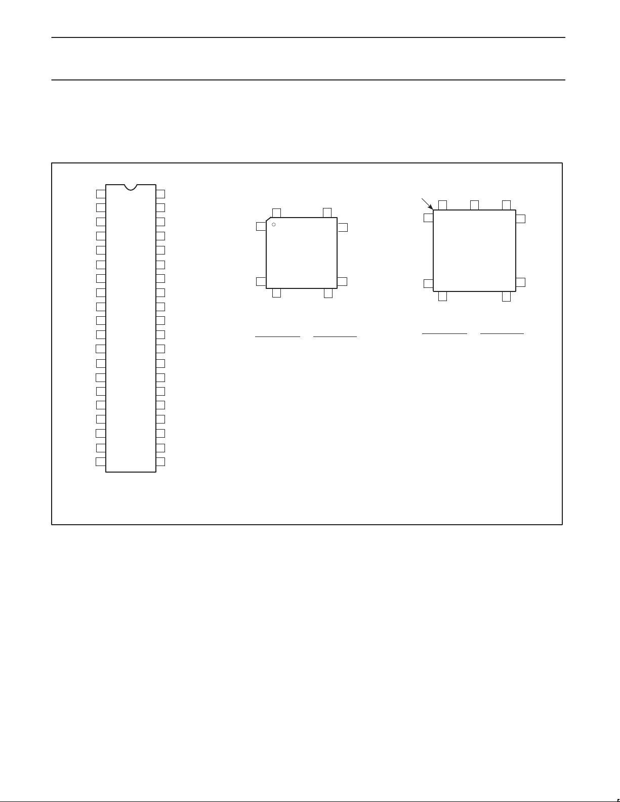
The SC26C92 is available in three package versions: 40-pin 0.6”
wide DIP, a 44-pin PLCC and 44–pin plastic quad flat pack (PQFP).
FEATURES
•Dual full-duplex independent asynchronous receiver/transmitters
•8 character FIFOs for each receiver and transmitter
•Programmable data format
– 5 to 8 data bits plus parity
– Odd, even, no parity or force parity
– 1, 1.5 or 2 stop bits programmable in 1/16-bit increments
•16-bit programmable Counter/Timer
•Programmable baud rate for each receiver and transmitter
selectable from:
– 27 fixed rates: 50 to 230.4k baud
– Other baud rates to 230.4k baud at 16X
– Programmable user-defined rates derived from a
programmable counter/timer
– External 1X or 16X clock
•Parity, framing, and overrun error detection
•False start bit detection
•Line break detection and generation
•Programmable channel mode
– Normal (full-duplex)
– Automatic echo
– Local loopback
– Remote loopback
– Multidrop mode (also called ‘wake-up’ or ‘9-bit’)
•Multi-function 7-bit input port
– Can serve as clock, modem, or control inputs
– Change of state detection on four inputs
– Inputs have typically >100k pull-up resistors
•Multi-function 8-bit output port
– Individual bit set/reset capability
– Outputs can be programmed to be status/interrupt signals
– FIFO states for DMA and modem interface
•Versatile interrupt system
– Single interrupt output with eight maskable interrupting
conditions
– Output port can be configured to provide a total of up to six
separate wire-ORable interrupt outputs
– Each FIFO can be programmed for four different interrupt levels
– Watch dog timer for each receiver
•Maximum data transfer rates:
1X – 1Mb/sec, 16X – 1Mb/sec
•Automatic wake-up mode for multidrop applications
•Start-end break interrupt/status
•Detects break which originates in the middle of a character
•On-chip crystal oscillator
•Power down mode
•Receiver timeout mode
•Single +5V power supply
•Powers up to emulate SCC2692
SC26C92
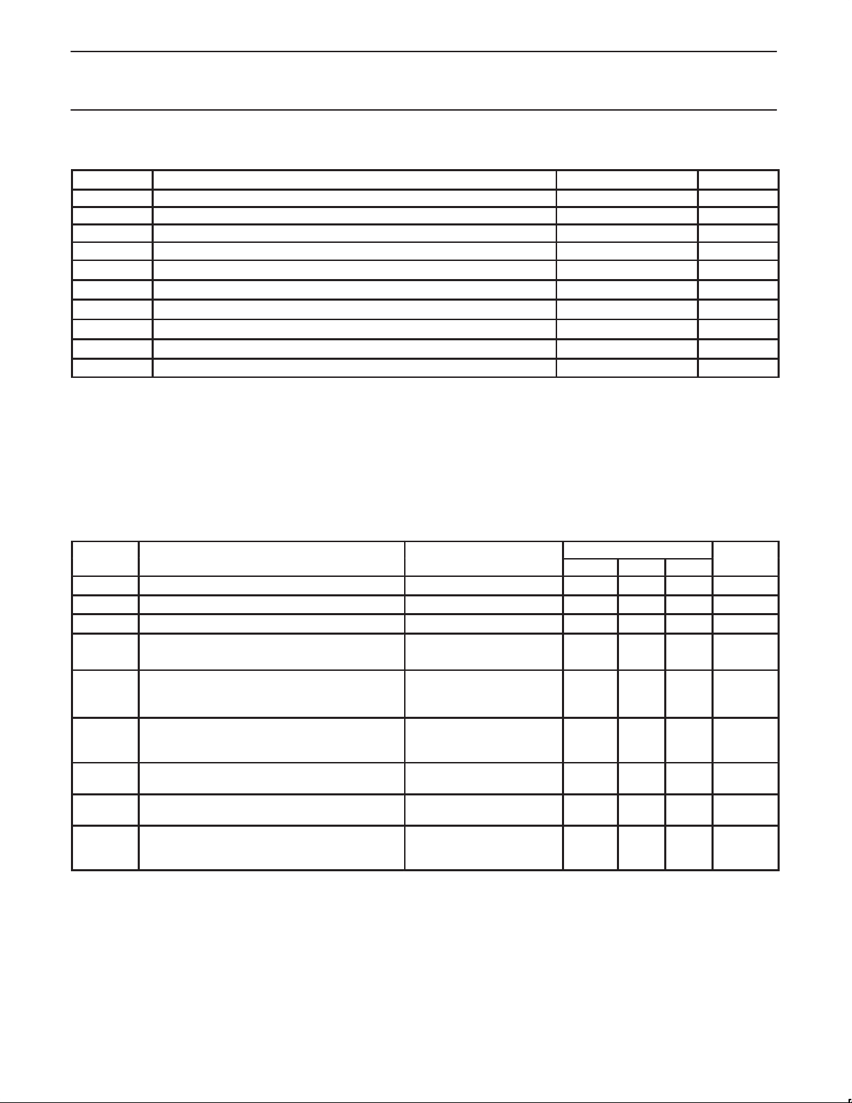
ORDERING INFORMATION
COMMERCIAL
VCC = +5V ±10%, TA = 0 to +70°C VCC = +5V ±10%, TA = -40 to +85°C
40-Pin Plastic Dual In-Line Package (DIP) SC26C92C1N SC26C92A1N SOT129-1
44-Pin Plastic Leaded Chip Carrier (PLCC) SC26C92C1A SC26C92A1A SOT187-2
44–Pin Plastic Quad Flat Pack (PQFP) SC26C92C1B SC26C92A1B SOT307–2
2000 Jan 31 853–1585 23061
1
2
INDUSTRIAL
Philips Semiconductors Product specification
Dual universal asynchronous receiver/transmitter (DUART)
NOTE:
1. Commercial devices are tested for the –40 to +85_C.
PIN CONFIGURATIONS
A0
IP3
A1
IP1
A2
A3
IP0
WRN
RDN
RxDB
TxDB
OP1
OP3
OP5
OP7
D1
D3
D5
D7
V
SS
1
2
3
4
5
6
7
8
9
10
DIP
11
12
13
14
15
16
17
18
19
40
39
38
37
36
35
34
33
32
31
30
29
28
27
26
25
24
23
22
2120
V
CC
IP4
IP5
IP6
IP2
CEN
RESET
X2
X1/CLK
RxDA
TxDA
OP0
OP2
OP4
OP6
D0
D2
D4
D6
INTRN
44
1
PQFP
11
12
TOP VIEW
PIN/FUNCTION PIN/FUNCTION
1 A3 23 N/C
2 IP0 24 OP6
3 WRN 25 OP4
4 RDN 26 OP2
5 RxDB 27 OP0
6 TxDB 28 TxDA
7 OP1 29 RxDA
8 OP3 30 X1/CLK
9 OP5 31 X2
10 OP7 32 RESET
11 N/C 33 CEN
12 D1 34 IP2
13 D3 35 IP6
14 D5 36 IP5
15 D7 37 IP4
16 GND 38 V
17 GND 39 V
18 INTRN 40 A0
19 D6 41 IP3
20 D4 42 A1
21 D2 43 IP1
22 D0 44 A2
34
33
23
22
CC
CC
INDEX
CORNER
SC26C92
6
7
17
18
PIN/FUNCTION PIN/FUNCTION
1NC 23NC
2 A0 24 INTRN
3 IP3 25 D6
4A1 26D4
5 IP1 27 D2
6A2 28D0
7 A3 29 OP6
8 IP0 30 OP4
9 WRN 31 OP2
10 RDN 32 OP0
11 RXDB 33 TXDA
12 NC 34 NC
13 TXDB 35 RXDA
14 OP1 36 X1/CLK
15 OP3 37 X2
16 OP5 38 RESET
17 OP7 39 CEN
18 D1 40 IP2
19 D3 41 IP6
20 D5 42 IP5
21 D7 43 IP4
22 V
1
PLCC
TOP VIEW
SS
44 V
40
28
CC
39
29
2000 Jan 31
SD00667
Figure 1. Pin Configurations
3
Philips Semiconductors Product specification
Dual universal asynchronous receiver/transmitter (DUART)
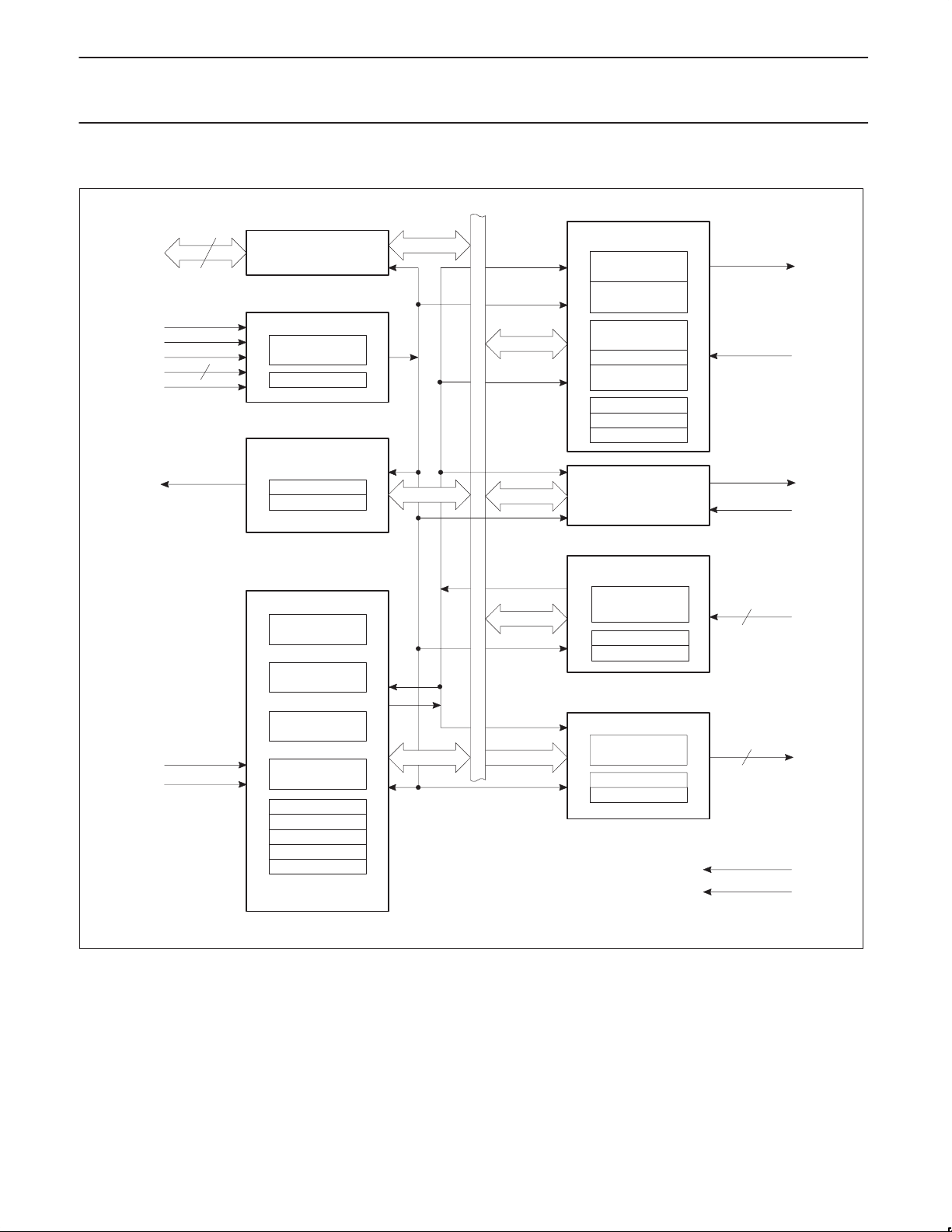
BLOCK DIAGRAM
D0–D7
RDN
WRN
CEN
A0–A3
RESET
INTRN
8
BUS BUFFER
OPERATION CONTROL
ADDRESS
4
DECODE
R/W CONTROL
INTERRUPT CONTROL
IMR
ISR
CHANNEL A
8 BYTE TRANSMIT
TRANSMIT
SHIFT REGISTER
8 BYTE RECEIVE
WATCH DOG TIMER
RECEIVE SHIFT
REGISTER
MRA0, 1, 2
CHANNEL B
(AS ABOVE)
FIFO
FIFO
CRA
SRA
SC26C92
TxDA
RxDA
TxDB
RxDB
X1/CLK
X2
TIMING
BAUD RATE
GENERATOR
CLOCK
SELECTORS
COUNTER/
TIMER
XTAL OSC
CSRA
CSRB
ACR
U
CTPL
CTPL
CONTROL
TIMING
INTERNAL DATABUS
Figure 2. Block Diagram
INPUT PORT
CHANGE OF
STATE
DETECTORS (4)
IPCR
ACR
OUTPUT PORT
FUNCTION
SELECT LOGIC
OPCR
OPR
7
8
IP0-IP6
OP0-OP7
V
CC
V
SS
SD00153
2000 Jan 31
4

Philips Semiconductors Product specification
SYMBOL
NAME AND FUNCTION
Dual universal asynchronous receiver/transmitter (DUART)
SC26C92
PIN DESCRIPTION
PKG
40,44
D0-D7 X I/O Data Bus: Bidirectional 3-State data bus used to transfer commands, data and status between the DUART
CEN X I Chip Enable: Active-Low input signal. When Low, data transfers between the CPU and the DUART are
WRN X I Write Strobe: When Low and CEN is also Low, the contents of the data bus is loaded into the addressed
RDN X I Read Strobe: When Low and CEN is also Low, causes the contents of the addressed register to be
A0-A3 X I Address Inputs: Select the DUART internal registers and ports for read/write operations.
RESET X I Reset: A High level clears internal registers (SRA, SRB, IMR, ISR, OPR, OPCR), puts OP0-OP7 in the
INTRN X O Interrupt Request: Active-Low, open-drain, output which signals the CPU that one or more of the eight
X1/CLK X I Crystal 1: Crystal connection or an external clock input. A crystal of a clock the appropriate frequency
X2 X I Crystal 2: Crystal connection. See Figure 7. If a crystal is not used this pin must be left open or not driving
RxDA X I Channel A Receiver Serial Data Input: The least significant bit is received first. “Mark” is High, “space” is Low.
RxDB X I Channel B Receiver Serial Data Input: The least significant bit is received first. “Mark” is High, “space” is Low.
TxDA X O Channel A Transmitter Serial Data Output: The least significant bit is transmitted first. This output is held
TxDB X O Channel B Transmitter Serial Data Output: The least significant bit is transmitted first. This output is
OP0 X O Output 0: General purpose output or Channel A request to send (RTSAN, active-Low). Can be
OP1 X O Output 1: General purpose output or Channel B request to send (RTSBN, active-Low). Can be
OP2 X O Output 2: General purpose output, or Channel A transmitter 1X or 16X clock output, or Channel A receiver
OP3 X O Output 3: General purpose output or open-drain, active-Low counter/timer output or Channel B transmitter
OP4 X O Output 4: General purpose output or Channel A open-drain, active-Low, RxA interrupt ISR[1] output.
OP5 X O Output 5: General purpose output or Channel B open-drain, active-Low, RxB interrupt ISR[5] output.
OP6 X O Output 6: General purpose output or Channel A open-drain, active-Low, TxA interrupt ISR[0] output.
OP7 X O Output 7: General purpose output, or Channel B open-drain, active-Low, TxB interrupt ISR[4] output.
IP0 X I Input 0: General purpose input or Channel A clear to send active-Low input (CTSAN). Pin has an internal
IP1 X I Input 1: General purpose input or Channel B clear to send active-Low input (CTSBN). Pin has an internal
IP2 X I Input 2: General purpose input or counter/timer external clock input. Pin has an internal VCC pull-up device
IP3 X I Input 3: General purpose input or Channel A transmitter external clock input (TxCA). When the external
IP4 X I Input 4: General purpose input or Channel A receiver external clock input (RxCA). When the external
IP5 X I Input 5: General purpose input or Channel B transmitter external clock input (TxCB). When the external
IP6 X I Input 6: General purpose input or Channel B receiver external clock input (RxCB). When the external
V
CC
GND X I Ground
X I Power Supply: +5V supply input.
PIN
TYPE
and the CPU. D0 is the least significant bit.
enabled on D0-D7 as controlled by the WRN, RDN and A0-A3 inputs. When High, places the D0-D7 lines
in the 3-State condition.
register. The transfer occurs on the rising edge of the signal.
presented on the data bus. The read cycle begins on the falling edge of RDN.
High state, stops the counter/timer, and puts Channels A and B in the inactive state, with the TxDA and
TxDB outputs in the mark (High) state. Sets MR pointer to MR1 and resets MR0.
maskable interrupting conditions are true. Requires a pullup resistor.
(nominally 3.6864 MHz) must be supplied at all times. For crystal connections see Figure 7, Clock Timing.
more than one TTL equivalent load.
in the “mark” condition when the transmitter is disabled, idle or when operating in local loopback mode.
“Mark” is High, “space” is Low.
held in the ‘mark’ condition when the transmitter is disabled, idle, or when operating in local loopback mode.
‘Mark’ is High, ‘space’ is Low.
deactivated automatically on receive or transmit.
deactivated automatically on receive or transmit.
1X clock output.
1X clock output, or Channel B receiver 1X clock output.
pull-up device supplying 1 to 4 mA of current.
V
CC
V
pull-up device supplying 1 to 4 mA of current.
CC
supplying 1 to 4 mA of current.
clock is used by the transmitter, the transmitted data is clocked on the falling edge of the clock. Pin has an
internal V
clock is used by the receiver, the received data is sampled on the rising edge of the clock. Pin has an
internal V
clock is used by the transmitter, the transmitted data is clocked on the falling edge of the clock. Pin has an
internal V
clock is used by the receiver, the received data is sampled on the rising edge of the clock. Pin has an
internal V
pull-up device supplying 1 to 4 mA of current.
CC
pull-up device supplying 1 to 4 mA of current.
CC
pull-up device supplying 1 to 4 mA of current.
CC
pull-up device supplying 1 to 4 mA of current.
CC
2000 Jan 31
5
Philips Semiconductors Product specification
Dual universal asynchronous receiver/transmitter (DUART)
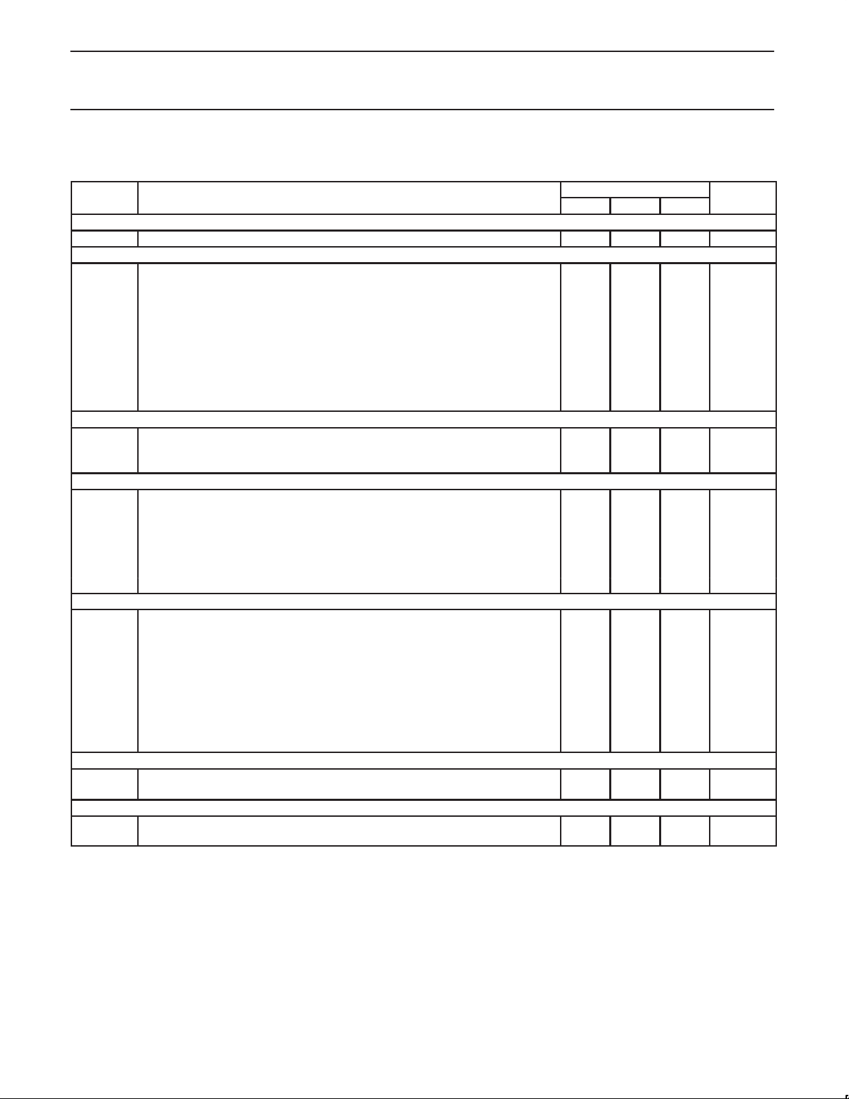
ABSOLUTE MAXIMUM RATINGS
SYMBOL
T
T
V
V
P
P
P
A
STG
CC
S
D
D
D
Operating ambient temperature range
Storage temperature range -65 to +150 °C
Voltage from VCC to GND
Voltage from any pin to GND
Package power dissipation (DIP40) 2.8 W
Package power dissipation (PLCC44) 2.4 W
Package power dissipation (PQFP44) 1.78 W
Derating factor above 25_C (PDIP40)
Derating factor above 25_C (PLCC44)
Derating factor above 25_C (PQFP44)
1
PARAMETER RATING UNIT
2
3
3
Note 4 °C
-0.5 to +7.0 V
-0.5 to VCC +0.5 V
22
19
14
SC26C92
mW/_C
mW/_C
mW/_C
NOTES:
1. Stresses above those listed under Absolute Maximum Ratings may cause permanent damage to the device. This is a stress rating only and
functional operation of the device at these or any other condition above those indicated in the operation section of this specification is not
implied.
2. For operating at elevated temperatures, the device must be derated based on +150°C maximum junction temperature.
3. This product includes circuitry specifically designed for the protection of its internal devices from damaging effects of excessive static
charge. Nonetheless, it is suggested that conventional precautions be taken to avoid applying any voltages larger than the rated maxima.
4. Parameters are valid over specified temperature range.
DC ELECTRICAL CHARACTERISTICS
VCC = 5V ± 10%, T
= –40_C to 85_C, unless otherwise specified.
A
1, 2
LIMITS
SYMBOL PARAMETER TEST CONDITIONS Min Typ Max UNIT
V
IL
V
IH
V
IH
V
OL
V
OH
I
IX1PD
I
ILX1
I
IHX1
I
I
I
OZH
I
OZL
I
ODL
I
ODH
I
CC
Input low voltage 0.8 V
Input high voltage (except X1/CLK) –40 to +85°C 2.5 V
Input high voltage (X1/CLK) 0.8 V
I
Output low voltage
Output high voltage (except OD outputs)
X1/CLK input current - power down
X1/CLK input low current - operating
X1/CLK input high current - operating
3
OL
I
OH
V
IN
V
= 2.4mA
= -400µA
= 0 to V
VIN = 0
= V
IN
CC
CC
V
CC
-0.5
-130
-0.5
CC
0.4 V
+0.5
130
Input leakage current:
All except input port pins
Input port pins
Output off current high, 3-State data bus
Output off current low , 3-State data bus
Open-drain output low current in off-state
Open-drain output high current in off-state
Power supply current
Operating mode
Power down mode
4
5
VIN = 0 to V
VIN = 0 to V
VIN = V
VIN = 0V –0.5
CC
CC
CC
VIN = 0
V
= V
IN
CC
CMOS input levels
CMOS input levels
-0.5
-8
–0.5
+0.5
+0.5
0.5 µA
0.5
5
2
10
15
NOTES:
1. Parameters are valid over specified temperature range.
2. Typical values are at +25°C, typical supply voltages, and typical processing parameters.
3. Test conditions for outputs: C
= 150pF, except interrupt outputs. Test conditions for interrupt outputs: CL = 50pF, R
L
= 2.7KΩ to VCC.
L
4. All outputs are disconnected. Inputs are switching between CMOS levels of VCC -0.2V and VSS + 0.2V.
5. See UART application note for power down currents of 5µA or less.
V
V
µA
µA
µA
µA
µA
µA
µA
µA
mA
mA
2000 Jan 31
6
Philips Semiconductors Product specification
Dual universal asynchronous receiver/transmitter (DUART)
AC CHARACTERISTICS
VCC = 5V ± 10%, T
= –40_C to 85_C, unless otherwise specified.
A
1, 2, 4
SC26C92
LIMITS
SYMBOL PARAMETER Min Typ
3
Max UNIT
Reset Timing (See Figure 3)
t
RES
Bus Timing
t
AS
t
AH
t
CS
t
CH
t
RW
t
DD
t
DF
t
DS
t
DH
t
RWD
RESET pulse width 200 ns
5
(See Figure 4)
A0-A3 setup time to RDN, WRN Low 10 ns
A0-A3 hold time from RDN, WRN Low 25 ns
CEN setup time to RDN, WRN Low 0 ns
CEN hold time from RDN, WRN High 0 ns
WRN, RDN pulse width 70 ns
Data valid after RDN Low 55 ns
Data bus floating after RDN High 25 ns
Data setup time before WRN or CEN High 25 ns
Data hold time after WRN or CEN High 0 ns
High time between reads and/or writes
5, 6
30 ns
Port Timing5 (See Figure 5)
t
PS
t
PH
t
PD
Port input setup time before RDN Low 0 ns
Port input hold time after RDN High 0 ns
OPn output valid from WRN High 100 ns
Interrupt Timing (See Figure 6)
INTRN (or OP3-OP7 when used as interrupts) negated from:
Read RxFIFO (RxRDY/FFULL interrupt) 100 ns
Write TxFIFO (TxRDY interrupt) 100 ns
t
IR
Reset command (break change interrupt) 100 ns
Stop C/T command (counter interrupt) 100 ns
Read IPCR (input port change interrupt) 100 ns
Write IMR (clear of interrupt mask bit) 100 ns
Clock Timing (See Figure 7)
t
CLK
f
CLK
t
CTC
f
CTC
t
RX
f
RX
t
TX
f
TX
X1/CLK High or Low time 50 ns
X1/CLK frequency 0.1 3.6864 8 MHz
CTCLK (IP2) High or Low time 55 ns
CTCLK (IP2) frequency 0 8 MHz
RxC High or Low time (16X) 30 ns
RxC frequency (16X)
(1X)
8
0
0
16
1
MHz
MHz
TxC High or Low time (16X) 30 ns
TxC frequency (16X)
(1X)
8
0
0
16
1
MHz
MHz
Transmitter T iming (See Figure 8)
t
TXD
t
TCS
TxD output delay from TxC external clock input on IP pin 60 ns
Output delay from TxC low at OP pin to TxD data output 5 30 ns
Receiver Timing (See Figure 9)
t
RXS
t
RXH
RxD data setup time before RxC high at external clock input on IP pin 50 ns
RxD data hold time after RxC high at external clock input on IP pin 50 ns
NOTES:
1. Parameters are valid over specified temperature range.
2. All voltage measurements are referenced to ground (GND). For testing, all inputs swing between 0.4V and 3.0V with a transition time of 5ns
maximum. For X1/CLK this swing is between 0.4V and 4.4V . All time measurements are referenced at input voltages of 0.8V and 2.0V and
output voltages of 0.8V and 2.0V , as appropriate.
3. Typical values are at +25°C, typical supply voltages, and typical processing parameters.
4. Test conditions for outputs: C
5. Timing is illustrated and referenced to the WRN and RDN inputs. Also, CEN may be the ‘strobing’ input. CEN and RDN (also CEN and
= 150pF, except interrupt outputs. Test conditions for interrupt outputs: CL = 50pF, R
L
= 2.7KΩ to VCC.
L
WRN) are ORed internally. The signal asserted last initiates the cycle and the signal negated first terminates the cycle.
6. If CEN is used as the ‘strobing’ input, the parameter defines the minimum High times between one CEN and the next. The RDN signal must
be negated for t
7. Minimum frequencies are not tested but are guaranteed by design. Crystal frequencies 2 to 4 MHz.
to guarantee that any status register changes are valid.
RWD
8. Clocks for 1X mode should be symmetrical.
2000 Jan 31
7

Philips Semiconductors Product specification
Dual universal asynchronous receiver/transmitter (DUART)
Block Diagram
The SC26C92 DUART consists of the following eight major sections:
data bus buffer, operation control, interrupt control, timing,
communications Channels A and B, input port and output port.
Refer to the Block Diagram.
Data Bus Buffer
The data bus buffer provides the interface between the external and
internal data buses. It is controlled by the operation control block to
allow read and write operations to take place between the controlling
CPU and the DUART.
Operation Control
The operation control logic receives operation commands from the
CPU and generates appropriate signals to internal sections to
control device operation. It contains address decoding and read and
write circuits to permit communications with the microprocessor via
the data bus.
Interrupt Control
A single active-Low interrupt output (INTRN) is provided which is
activated upon the occurrence of any of eight internal events.
Associated with the interrupt system are the Interrupt Mask Register
(IMR) and the Interrupt Status Register (ISR). The IMR can be
programmed to select only certain conditions to cause INTRN to be
asserted. The ISR can be read by the CPU to determine all
currently active interrupting conditions.
Outputs OP3-OP7 can be programmed to provide discrete interrupt
outputs for the transmitter, receivers, and counter/timer.
When OP3 to OP7 are programmed as interrupts, their output
buffers are changed to the open drain active low configuration.
These pins may be used for DMA and modem control.
Counter–Timer
The Counter/Timer is a programmable 16–bit divider that is used for
generating miscellaneous clocks or generating timeout periods.
These clocks may be used by any or all of the receivers and transmitters in the DUART or may be directed to an I/O pin for miscellaneous use.
Counter/Timer programming
The counter timer is a 16–bit programmable divider that operates in
one of three modes: counter, timer, and time out.
•Timer mode generates a square wave.
•Counter mode generates a time delay.
•Time out mode counts time between received characters.
The C/T uses the numbers loaded into the Counter/Timer Lower
Register (CTPL) and the Counter/Timer Upper Register (CTPU) as
its divisor. The counter timer is controlled with six commands: Start/
Stop C/T, Read/Write Counter/Timer lower register and Read/Write
Counter/Timer upper register. These commands have slight differences depending on the mode of operation. Please see the detail of
the commands under the CTPL/CTPU register descriptions.
Baud Rate Generation with the C/T
When the timer is selected as baud rates for receiver or transmitter
via the Clock Select register their output will be configured as a 16x
clock. Therefore one needs to program the timer to generate a
clock 16 times faster than the data rate. The formula for calculating
’n’, the number loaded to the CTPU and CTPL registers, based on a
particular input clock frequency is shown below.
For the timer mode the formula is as follows:
SC26C92
TIMING CIRCUITS
Crystal Clock
The timing block consists of a crystal oscillator, a baud rate
generator, a programmable 16-bit counter/timer, and four clock
selectors. The crystal oscillator operates directly from a crystal
connected across the X1/CLK and X2 inputs. If an external clock of
the appropriate frequency is available, it may be connected to
X1/CLK. The clock serves as the basic timing reference for the
Baud Rate Generator (BRG), the counter/timer, and other internal
circuits. A clock signal within the limits specified in the
specifications section of this data sheet must always be supplied to
the DUART.
If an external is used instead of a crystal, X1 should be driven using
a configuration similar to the one in Figure 7.
BRG
The baud rate generator operates from the oscillator or external
clock input and is capable of generating 27 commonly used data
communications baud rates ranging from 50 to 38.4K baud.
Programming bit 0 of MR0 to a “1” gives additional baud rates to
230.4kB. These will be in the 16X mode. A 3.6864MHz crystal or
external clock must be used to get the standard baud rates. The
clock outputs from the BRG are at 16X the actual baud rate. The
counter/timer can be used as a timer to produce a 16X clock for any
other baud rate by counting down the crystal clock or an external
clock. The four clock selectors allow the independent selection, for
each receiver and transmitter, of any of these baud rates or external
timing signal.
Clockinputfrequency
n=
2 16 Baudratedesired
NOTE: ‘n’ may not assume values of 0 and 1.
The frequency generated from the above formula will be at a rate 16
times faster than the desired baud rate. The transmitter and receiver state machines include divide by 16 circuits, which provide the
final frequency and provide various timing edges used in the qualifying the serial data bit stream. Often this division will result in a non–
integer value: 26.3 for example. One may only program integer
numbers to a digital divider. There for 26 would be chosen. If 26.7
were the result of the division then 27 would be chosen. This gives
a baud rate error of 0.3/26.3 or 0.3/26.7 that yields a percentage
error of 1.14% or 1.12% respectively, well within the ability of the
asynchronous mode of operation. Higher input frequency to the
counter reduces the error effect of the fractional division
One should be cautious about the assumed benign effects of small
errors since the other receiver or transmitter with which one is communicating may also have a small error in the precise baud rate. In
a ”clean” communications environment using one start bit, eight data
bits and one stop bit the total difference allowed between the transmitter and receiver frequency is approximately 4.6%. Less than
eight data bits will increase this percentage.
Communications Channels A and B
Each communications channel of the SC26C92 comprises a
full-duplex asynchronous receiver/transmitter (UART). The
2000 Jan 31
8

Philips Semiconductors Product specification
Dual universal asynchronous receiver/transmitter (DUART)
operating frequency for each receiver and transmitter can be
selected independently from the baud rate generator, the
counter/timer, or from an external input.
The transmitter accepts parallel data from the CPU, converts it to a
serial bit stream, inserts the appropriate start, stop, and optional
parity bits and outputs a composite serial stream of data on the TxD
output pin.
The receiver accepts serial data on the RxD pin, converts this serial
input to parallel format, checks for start bit, stop bit, parity bit (if any),
or break condition and sends an assembled character to the CPU
via the receive FIFO. Three status bits (Break Received, Framing
and Parity Errors) are also FIFOed with each data character.
Input Port
The inputs to this unlatched 7-bit port can be read by the CPU by
performing a read operation at address H’D’. A High input results in
a logic 1 while a Low input results in a logic 0. D7 will always read
as a logic 1. The pins of this port can also serve as auxiliary inputs
to certain portions of the DUART logic or modem and DMA control.
Four change-of-state detectors are provided which are associated
with inputs IP3, IP2, IP1 and IP0. A High-to-Low or Low-to-High
transition of these inputs, lasting longer than 25 - 50µs, will set the
corresponding bit in the input port change register. The bits are
cleared when the register is read by the CPU. Any change-of-state
can also be programmed to generate an interrupt to the CPU.
The input port pulse detection circuitry uses a 38.4KHz sampling
clock derived from one of the baud rate generator taps. This results
in a sampling period of slightly more than 25µs (this assumes that
the clock input is 3.6864MHz). The detection circuitry, in order to
guarantee that a true change in level has occurred, requires two
successive samples at the new logic level be observed. As a
consequence, the minimum duration of the signal change is 25µs if
the transition occurs “coincident with the first sample pulse”. The
50µs time refers to the situation in which the change-of-state is “just
missed” and the first change-of-state is not detected until 25µs later.
All the IP pins have a small pull-up device that will source 1 to 4 mA
of current from V
connections if they are not used.
V
CC
. These pins do not require pull-up devices or
CC
Output Port
The output ports are controlled from five places: the OPCR register,
SOPR, ROPR, the MR registers and the command register (CR).
The OPCR register controls the source of the data for the output
ports OP2 through OP7. The data source for output ports OP0 and
OP1 is controlled by the MR and CR registers. Normally the data
source for the OP pins is from the OPR register. The OP pin drive
the inverted level (complement) of the OPR register. Example:
when the SOPR is used to set the OPR bit to a logical 1 then the
associated OP pin will drive a logical 0.
The content of the OPR register is controlled by the “Set Output Port
Bits Command” and the “Reset Output Bits Command”. These commands are at E and F, respectively. When these commands are
used, action takes place only at the bit locations where ones exist.
For example, a one in bit location 5 of the data word used with the
“Set Output Port Bits” command will result in OPR(5) being set to
one. The OP5 would then be set to zero (V
bit position 5 of the data word associated with the “Reset Output
Ports Bits” command would set OPR(5) to zero and, hence, the pin
OP5 to a one (Vdd).
Please note that these pins drive both high and low. However when
they are programmed to represent interrupt type functions (such as
SS ). Similarly, a one in
RxRDY) they will be switched to an open drain configuration. In this
configuration an external pull–up device will be required
OPERATION
Transmitter
The SC26C92 is conditioned to transmit data when the transmitter is
enabled through the command register. The SC26C92 indicates to
the CPU that it is ready to accept a character by setting the TxRDY
bit in the status register. This condition can be programmed to
generate an interrupt request at OP0, OP1 and INTRN. When the
transmitter is initially enabled the TxRDY and TxEMT bits will be set
in the status register. When a character is loaded to the transmit
FIFO the TxEMT bit will be reset. The TxEMT will not set until: 1)
the transmit FIFO is empty and the transmit shift register has
finished transmitting the stop bit of the last character written to the
transmit FIFO, or 2) the transmitter is disabled and then re–enabled.
The TxRDY bit is set whenever the transmitter is enabled and the
TxFIFO is not full. Data is transferred from the holding register to
transmit shift register when it is idle or has completed transmission
of the previous character. Characters cannot be loaded into the
TxFIFO while the transmitter is disabled.
The transmitter converts the parallel data from the CPU to a serial
bit stream on the TxD output pin. It automatically sends a start bit
followed by the programmed number of data bits, an optional parity
bit, and the programmed number of stop bits. The least significant
bit is sent first. Following the transmission of the stop bits, if a new
character is not available in the TxFIFO, the TxD output remains
High and the TxEMT bit in the Status Register (SR) will be set to 1.
Transmission resumes and the TxEMT bit is cleared when the CPU
loads a new character into the TxFIFO.
If the transmitter is disabled, it continues operating until the character currently being transmitted and any characters in the TxFIFO
including parity and stop bit(s) have been completed.
Note the differences between the transmitter disable and the transmitter reset: reset stops all transmission immediately, effectively
clears the TxFIFO and resets all status and Tx interrupt conditions.
Transmitter disable clears all Tx status and interrupts BUT allows
the Tx to complete the transmission of all data in the TxFIFO and in
the shift register. While the Tx is disabled the TxFIFO can not be
loaded with data.
The transmitter can be forced to send a continuous Low condition by
issuing a send break command from the command register. The
transmitter output is returned to the normal high with a stop break
command.
The transmitter can be reset through a software command. If it is
reset, operation ceases immediately and the transmitter must be
enabled through the command register before resuming operation.
If the CTS option is enabled (MR2[4] = 1), the CTSN input at IP0 or
IP1 must be low in order for the character to be transmitted. The
transmitter will check the state of the CTS input at the beginning of
each character transmitted. If it is found to be High, the transmitter
will delay the transmission of any following characters until the CTS
has returned to the low state. CTS going high during the serialization of a character will not affect that character.
Transmitter “RS485 turnaround”
The transmitter can also control the RTSN outputs, OP0 or OP1 via
MR2[5]. When this mode of operation is set, the meaning of the
OP0 and OP1 signal will usually be ‘end of message’. See
description of the MR2[5] bit for more detail.
SC26C92
2000 Jan 31
9

Philips Semiconductors Product specification
Dual universal asynchronous receiver/transmitter (DUART)
This feature may be used automatically “turnaround” a transceiver
when operating in a simplex system.
Transmitter Disable Note (W.R.T. Turnaround)
When the TxEMT bit is set the sequence of instructions: enable
transmitter — load transmit holding register — disable transmitter
will often result in nothing being sent. In the condition of the TxEMT
being set do not issue the disable until the TxRDY bit goes active
again after the character is loaded to the TxFIFO. The data is not
sent if the time between the end of loading the transmit holding
register and the disable command is less that 3/16 bit time in the
16x mode. One bit time in the 1x mode.
This is sometimes the condition when the RS485 automatic “turnaround” is enabled . It will also occur when only one character is to
be sent and it is desired to disable the transmitter immediately after
the character is loaded.
In general, when it is desired to disable the transmitter before the
last character is sent AND the TxEMT bit is set in the status register
be sure the TxRDY bit is active immediately before issuing the
transmitter disable instruction. (TxEMT is always set if the transmitter has underrun or has just been enabled), TxRDY sets at the end
of the “start bit” time. It is during the start bit that the data in the
transmit holding register is transferred to the transmit shift register.
Transmitter Flow control
The transmitter may be controlled by the CTSN input when enabled
by MR2(4). The CTSN input would be connected to RTSN output of
the receiver to which it is communicating. See further description in
the MR 1 and MR2 register descriptions.
Receiver
The SC26C92 is conditioned to receive data when enabled through
the command register. The receiver looks for a High-to-Low
(mark-to-space) transition of the start bit on the RxD input pin. If a
transition is detected, the state of the RxD pin is sampled each 16X
clock for 7-1/2 clocks (16X clock mode) or at the next rising edge of
the bit time clock (1X clock mode). If RxD is sampled High, the start
bit is invalid and the search for a valid start bit begins again. If RxD
is still Low, a valid start bit is assumed and the receiver continues to
sample the input at one bit time intervals at the theoretical center of
the bit, until the proper number of data bits and parity bit (if any)
have been assembled, and one stop bit has been detected. The
least significant bit is received first. The data is then transferred to
the Receive FIFO and the RxRDY bit in the SR is set to a 1. This
condition can be programmed to generate an interrupt at OP4 or
OP5 and INTRN. If the character length is less than 8 bits, the most
significant unused bits in the RxFIFO are set to zero.
After the stop bit is detected, the receiver will immediately look for
the next start bit. However, if a non-zero character was received
without a stop bit (framing error) and RxD remains Low for one half
of the bit period after the stop bit was sampled, then the receiver
operates as if a new start bit transition had been detected at that
point (one-half bit time after the stop bit was sampled).
The parity error, framing error, and overrun error (if any) are strobed
into the SR at the received character boundary, before the RxRDY
status bit is set. If a break condition is detected (RxD is Low for the
entire character including the stop bit), a character consisting of all
zeros will be loaded into the RxFIFO and the received break bit in
the SR is set to 1. The RxD input must return to high for two (2)
clock edges of the X1 crystal clock for the receiver to recognize the
end of the break condition and begin the search for a start bit. This
will usually require a high time of one X1 clock period or 3 X1
edges since the clock of the controller is not synchronous to
the X1 clock.
Receiver FIFO
The RxFIFO consists of a First-In-First-Out (FIFO) stack with a
capacity of eight characters. Data is loaded from the receive shift
register into the topmost empty position of the FIFO. The RxRDY bit
in the status register is set whenever one or more characters are
available to be read, and a FFULL status bit is set if all eight stack
positions are filled with data. Either of these bits can be selected to
cause an interrupt. A read of the RxFIFO outputs the data at the top
of the FIFO. After the read cycle, the data FIFO and its associated
status bits (see below) are ‘popped’ thus emptying a FIFO position
for new data.
Receiver Status Bits
There are five (5) status bits that are evaluated with each byte (or
character) received: received break, framing error, parity error, overrun error, and change of break. The first three are appended to
each byte and stored in the RxFIFO. The last two are not necessarily related to the byte being received or a byte that is in the RxFIFO.
They are however developed by the receiver state machine.
The received break, framing error, parity error and overrun error (if
any) are strobed into the RxFIFO at the received character boundary, before the RxRDY status bit is set. For character mode (see
below) status reporting the SR (Status Register) indicates the condition of these bits for the character that is the next to be read from the
FIFO
The ”received break” will always be associated with a zero byte in
the RxFIFO. It means that zero character was a break character
and not a zero data byte. The reception of a break condition will
always set the ”change of break” (see below) status bit in the Interrupt Status Register (ISR). The Change of break condition is reset
by a reset error status command in the command register
Break Detection
If a break condition is detected (RxD is Low for the entire character
including the stop bit), a character consisting of all zeros will be
loaded into the RxFIFO and the received break bit in the SR is set to
1. The change of break bit also sets in the ISR The RxD input must
return to high for two (2) clock edges of the X1 crystal clock for the
receiver to recognize the end of the break condition and begin the
search for a start bit.
This will usually require a high time of one X1 clock period or 3
X1 edges since the clock of the controller is not synchronous
to the X1 clock.
Framing Error
A framing error occurs when a non–zero character whose parity bit
(if used) and stop; bit are zero. If RxD remains low for one half of
the bit period after the stop bit was sampled, then the receiver
operates as if the start bit of the next character had been detected.
The parity error indicates that the receiver–generated parity was not
the same as that sent by the transmitter.
The framing, parity and received break status bits are reset when
the associated data byte is read from the RxFIFO since these “error”
conditions are attached to the byte that has the error
Overrun Error
The overrun error occurs when the RxFIFO is full, the receiver shift
register is full, and another start bit is detected. At this moment the
receiver has 9 valid characters and the start bit of the 10
SC26C92
th
has been
2000 Jan 31
10
 Loading...