


INTEGRATED CIRCUITS
SC26C562
CMOS dual universal serial
communications controller (CDUSCC)
Product specification
Supersedes data of 1995 May 01
IC19 Data Handbook
1998 Sep 04

Philips Semiconductors Product specification
CMOS dual universal serial communications controller
(CDUSCC)
DESCRIPTION
The Philips Semiconductors SC26C562 Dual Universal Serial
Communications Controller (CDUSCC) is a single-chip CMOS-LSI
communications device that provides two independent,
multi-protocol, full-duplex receiver/transmitter channels in a single
package. It supports bit-oriented and character-oriented (byte count
and byte control) synchronous data link controls as well as
asynchronous protocols. The SC26C562 interfaces to synchronous
bus MPUs and is capable of program-polled, interrupt driven,
block-move or DMA data transfers.
The SC26C562 (CDUSCC) is (PIN) hardware and (REGISTER)
software compatible with the existing SCN26562 (DUSCC).
CDUSCC will automatically configure to the NMOS DUSCC register
map (default mode) on power up.
The operating mode and data format of each channel can be
programmed independently. Each channel consists of a receiver, a
transmitter, a 16-bit multifunction counter/timer, a digital
phase-locked loop (DPLL), a parity/CRC generator and checker, and
associated control circuits. The two channels share a common bit
rate generator (BRG), operating directly from a crystal or an external
clock, which provides sixteen common bit rates simultaneously. The
operating rate for the receiver and transmitter of each channel can
be independently selected from the BRG, the DPLL, the
counter/timer, or from an external 1X or 16X clock, making the
CDUSCC well-suited for dual-speed channel applications. Data
rates up to 10Mbits per second are supported.
The transmitter and receiver each contain a sixteen-deep FIFO with
appended transmitter command and receiver status bits and a shift
register. This permits reading and writing of up to sixteen characters
at a time, minimizing the potential of receiver overrun or transmitter
underrun, and reducing interrupt or DMA overhead. In addition, a
flow control capability is provided to disable a remote transmitter
when the FIFO of the local receiving device is full.
Two modem control inputs (DCD and CTS) and three modem
control outputs (RTS and two general purpose) are provided.
Because the modem control inputs and outputs are general purpose
in nature, they can be optionally programmed for other functions.
The SC26C562 CDUSCC is optimized to interface with processors
using a synchronous bus interface, such as the 8086, and iAPX86
family. For systems using an asynchronous bus, such as the 68000
and 68010, refer to the SC68C562 documentation.
Refer to the CMOS Dual Universal Serial Communication Controller
(CDUSCC) User’s Manual for a complete operational description.
FEA TURES
General Features
•Dual full-duplex synchronous/ asynchronous receiver and
transmitter
•Multi-protocol operation
– BOP: HDLC/ADCCP, SDLC, SDLC loop, X.25 or X.75 link level,
etc.
– COP: Single SYNC, dual SYNC, BiSYNC, DDCMP
– ASYNC: 5-8 bits plus optional parity
•Sixteen character receive and transmit FIFOs with interrupt
threshold control
•FIFO’ed status bits
•Watchdog timer
•0 to 10 Mbit/sec data rate
•Programmable bit rate for each receiver and transmitter selectable
from:
– 19 fixed rates: 50 to 64K baud
– One user-defined rate derived from programmable
counter/timer
– External 1X or 16X clock
– Digital phase-locked loop
•Parity and FCS (frame check sequence LRC or CRC) generation
and checking
•Programmable data encoding/decoding: NRZ, NRZI, FM0, FM1,
Manchester
•Programmable channel mode: full- or half-duplex, auto-echo, or
local loopback
•Programmable data transfer mode: polled, interrupt, DMA, wait
•DMA interface
– Compatible with Synchronous and Asynchronous bus DMA
controllers
– Half- or full-duplex operation
– Single or dual address data transfers
– Automatic frame termination on counter/ timer terminal count or
DMA DONE (EOPN)
•Transmit path clear status
•High speed data bus interface: 160ns bus cycle
•DPLL operation up to 312.5kHz with internal clock
•Interrupt capabilities
– Vector output (fixed or modified by status)
– Individual interrupt enable bits
– Programmable internal priorities
– Maskable interrupt conditions
– 80XX/X compatible
•Multi-function programmable 16-bit counter/timer
– Bit rate generator
– Event counter
– Count received or transmitted characters
– Delay generator
– Automatic bit length measurement
•Modem controls
– RTS, CTS, DCD, and up to four general purpose I/O pins per
channel
– CTS and DCD programmable auto-enables for Tx and Rx
– Programmable interrupt on change of CTS or DCD
•On-chip oscillator for crystal
•TTL compatible
•Single +5V power supply
Asynchronous Mode Features
•Character length: 5 to 8 bits
SC26C562
1998 Sep 04 853-1663 19973
2
Philips Semiconductors Product specification
SYMBOL
PARAMETER
UNIT
CMOS dual universal serial communications controller
(CDUSCC)
•Odd or even parity, no parity, or force parity
•Up to two stop bits programmable in 1/16-bit increments
•1X or 16X Rx and Tx clock factors
•Parity, overrun and framing error detection
•False start bit detection
•Break generation with handshake for counting break characters
•Detection of start and end of received break
•Character compare with optional interrupt on match
•Transmit and receive up to 10Mbps at 1x or 1Mbps at 16x data
rates
Bit-Oriented Protocol
•Character length: 5 to 8 bits
•Detection and transmission of residual character: 0–7 bits
•Automatic switch to programmed character length for I field
•Zero insertion and deletion
•Optional opening PAD transmission
•Detection and generation of FLAG, ABORT, and IDLE bit patterns
•Transmit 7 or 8 bit ABORT
•Detection and generation of shared (single) FLAG between
frames
•Detection of overlapping (shared zero) FLAGs
•Idle in MARK or FLAGs
•Secondary address recognition including group and global
address
•Single- or dual-octet secondary address
•Extended address and control fields
•Short frame rejection for receiver
•Detection and notification of received end of message
•CRC generation and checking
•SDLC loop mode capability
Character-Oriented Protocols
•Character length: 5 to 8 bits
•Odd or even parity, no parity, or force parity
•LRC or CRC generation and checking
•Optional opening PAD transmission
•One or two SYN characters
•External sync capability
•SYN detection and optional stripping
•SYN or MARK line-fill or underrun
•Idle in MARK or SYNs
•Parity, FCS, overrun and underrun error detection
•Optional SYNC exclusion from FCS
•BISYNC features
– EBCDIC or ASCII header, text and control messages
– SYN, DLE stripping
– EOM (end of message) detection and transmission
– Auto transparency mode switching
– Auto hunt after receipt of EOM sequence (with closing PAD
check after EOT or NAK)
– Control character sequence detection for both transparent and
normal text
– Parity generation for data and LRC characters
SC26C562
ORDERING INFORMATION
COMMERCIAL INDUSTRIAL
DESCRIPTION
48-Pin Plastic Dual In-Line Package (DIP) SC26C562C1N Not available SOT240-1
52-Pin Plastic Leaded Chip Carrier (PLCC) Package SC26C562C1A SC26C562A8A SOT238-3
ABSOLUTE MAXIMUM RATINGS
T
A
T
STG
V
CC
V
S
1998 Sep 04
Operating ambient temperature
Storage temperature -65 to +150 -65 to +150 °C
Voltage from VCC to GND
Voltage from any pin to ground
1
2
3
3
Serial Data Rate =
10Mbps Maximum
RATING
COMMERCIAL INDUSTRIAL
0 to +70 -40 to +85 °C
–0.5 to +7.0 –0.5 to +7.0 V
–0.5 to VCC +0.5 –0.5 to VCC +0.5 V
3
Serial Data Rate =
8Mbps Maximum
DWG #
Philips Semiconductors Product specification
CMOS dual universal serial communications controller
(CDUSCC)
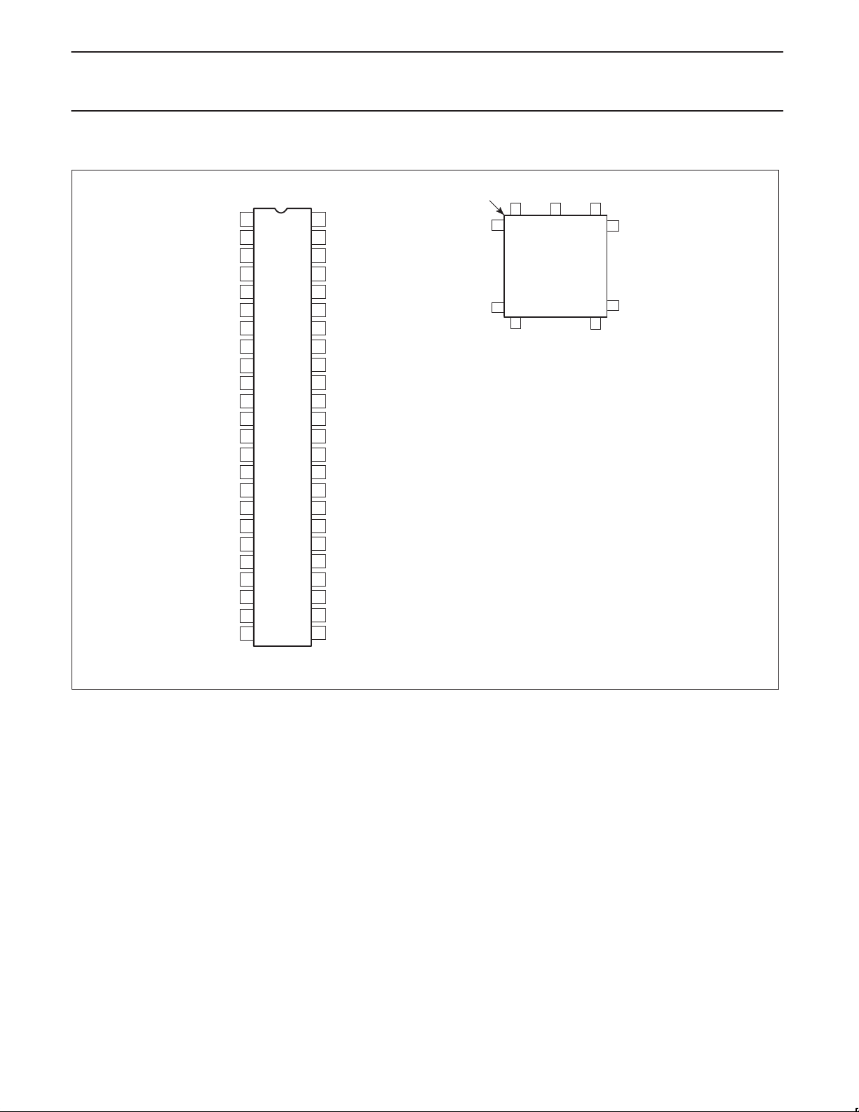
PIN CONFIGURATIONS
IACKN
RTxDAKBN/
GPI1BN
IRQN
RDYN
RTSBN/
SYNOUTBN
TRxCB
RTxCB
DCDBN/
SYNIBN
RxDB
TxDB
TxDAKBN/
GPI2BN
RTxDRQBN/
GPO1BN
TxDRQBN/
GPO2BN/RTSBN
CTSBN/LCBN
RDN
RESETN
GND
1
2
A3
3
A2
4
A1
5
6
7
8
9
10
11
12
13
14
15
16
17
18
D7
19
D6
20
D5
21
D4
22
23
24
N PACKAGE
DIP
48
V
CC
47
A4
46
A5
45
A6
RTxDAKAN/
44
GPI1AN
43
X1/CLK
42
X2
RTSAN/
41
SYNOUTAN
40
TRxCA
39
RTxCA
DCDAN/
38
SYNIAN
37
RxDA
36
TxDA
TxDAKAN/
35
GPI2AN
RTxDRQAN/
34
GPO1AN
TxDRQAN/
33
GPO2AN/RTSAN
32
CTSAN/LCAN
31
D0
30
D1
29
D2
28
D3
27
EOPN
26
WRN
25
CEN
INDEX
CORNER
7
8
20
21
PIN FUNCTION PIN FUNCTION
1 IACKN 27 CEN
2 A3 28 WRN
3 A2 29 EOPN
4A1 30D3
5 RTxDAKBN/ 31 D2
GPI1BN 32 D1
6 IRQN 33 D0
7NC 34NC
8 RDYN 35 CTSAN/LCAN
9 RTSBN/ 36 TxDRQAN/
SYNOUTBN GPO2AN/RTSAN
10 TRxCB 37 RTxDRQAN/
11 RTxCB GPO1AN
12 DCDBN/ 38 TxDAKAN/
SYNIBN GPI2AN
13 NC 39 TxDA
14 RxDB 40 RxDA
15 TxDB 41 NC
16 TxDAKBN/ 42 DCDAN/
GPI2BN SYNIAN
17 RTxDRQBN/ 43 RTxCA
GPO1BN 44 TRxCA
18 TxDRQBN/ 45 RTSAN/
GPO2BN/RTSBN SYNOUTAN
19 CTSBN/LCBN 46 X2
20 D7 47 X1/CLK
21 D6 48 RTxDAKAN/
22 D5 GPI1AN
23 D4 49 A6
24 RDN 50 A5
25 RESETN 51 A4
26 GND 52 V
A PACKAGE
1
PLCC
TOP VIEW
SC26C562
47
46
34
33
CC
SD00203
1998 Sep 04
Figure 1. Pin Configurations
4
Philips Semiconductors Product specification
CMOS dual universal serial communications controller
(CDUSCC)
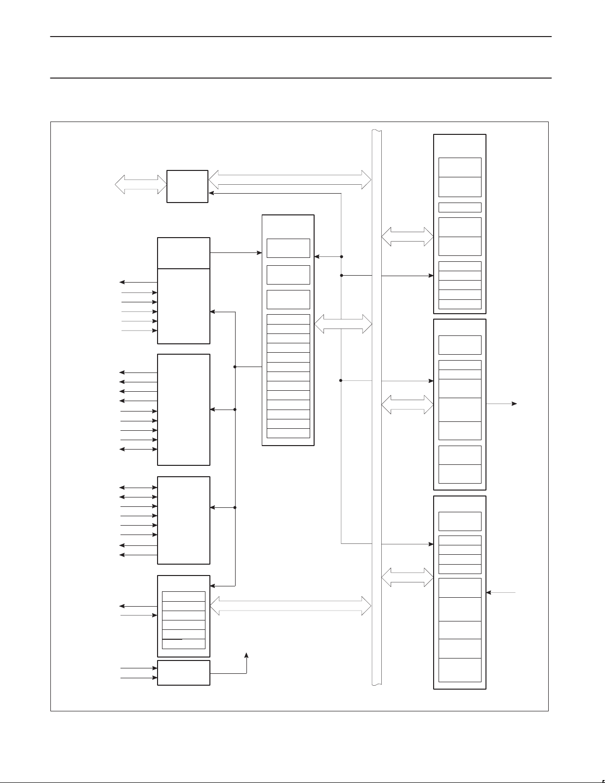
BLOCK DIAGRAM
D0–D7
RDYN
WRN
RDN
A1–A6
CEN
RESETN
RTxDRQAN/GPO1AN
RTxDRQBN/GPO1BN
TxDRQAN/GPO2AN
TxDRQBN/GPO2BN
RTxDAKAN/GPI1AN
RTxDAKBN/GPI1BN
TxDAKAN/GPI2AN
TxDAKBN/GPI2BN
EOPN
TRxCA/B
RTxCA/B
CTSAN/LCAN
CTSBN/LCBN
DCDBN/SYNIBN
DCDAN/SYNIAN
RTSBN/SYNOUTBN
RTSAN/SYNOUTAN
IRQN
IACKN
X1/CLK
X2
BUS
BUFFER
A7 CONTROL
LOGIC
MPU
INTERFACE
DMA
INTERFACE
SPECIAL
FUNCTION
PINS
INTERRUPT
CONTROL
ICRA/B
IERA/B
IVRM
IER1 A/B
IER2 A/B
IER3 A/B
OSCILLATOR
A7
CDUSCC
LOGIC
INTERFACE/
OPERATION
CONTROL
ADDRESS
DECODE
R/W
DECODE
DMA
CONTROL
CCRA/B
PCRA/B
RSRA/B
TRSRA/B
ICTSRA/B
GSR
CMR1A/B
CMR2A/B
OMRA/B
TRCR A/B
FTLR A/B
TRMR A/B
CID
CONTROL
INTERNAL BUS
CHANNEL
MODE AND
TIMING A/B
DPLL CLK
MUX A/B
DPLLA/B
BRG
COUNTER
TIMER A/B
C/T CLK
MUX A/B
CTCRA/B
CTPRHA/B
CTPRLA/B
CTHA/B
CTLA/B
TRANSMIT
A/B
TRANS CLK
MUX
TPRA/B
TTRA/B
TX SHIFT
REG
TRANSMIT
16 DEEP
FIFO
TELR
A/B
CRC
GENERATOR
SPEC CHAR
GEN LOGIC
RECEIVER
A/B
RCVR CLK
MUX
RPRA/B
RTRA/B
S1RA/B
S2RA/B
RCVR
SHIFT REG
RECEIVER
16 DEEP
FIFO
RFLR
A/B
CRC
ACCUM
BISYNC
COMPARE
LOGIC
SC26C562
TxD A/B
RxD A/B
1998 Sep 04
SD00239
Figure 2. Block Diagram
5
Philips Semiconductors Product specification
MNEMONIC
TYPE
NAME AND FUNCTION
CMOS dual universal serial communications controller
(CDUSCC)
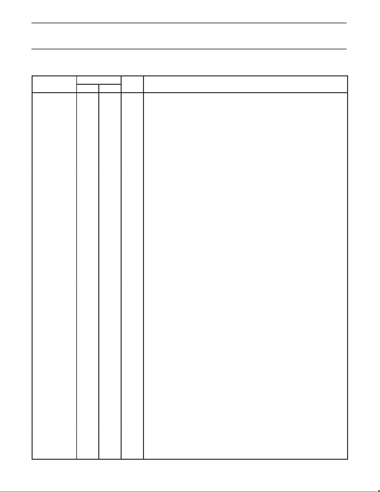
PIN DESCRIPTION
PIN NO.
DIP PLCC
A1–A6 4-2,
47-45
D0–D7 31-28,
21-18
RDN 22 24 I Read Strobe: Active-low input. When active and CSN is also active, causes the content
WRN 26 28 I Write Strobe: Active-low input. When active and CSN is also active, the content of the
CSN 25 27 I Chip Select: Active-low input. When active, data transfers between the CPU and the
RDYN 7 8 O Ready: Active-low, open drain. Used to synchronize data transfers between the CPU and
IRQN 6 6 O Interrupt Request: Active-low, open-drain. This output is asserted upon occurrence of
IACKN 1 1 I Interrupt Acknowledge: Active-low. When IACKN is asserted, the CDUSCC responds
X1/CLK 43 47 I Crystal or External Clock: When using the crystal oscillator, the crystal is connected
X2 42 46 O Crystal 2: Connection for other side of crystal. When a crystal is used, a capacitor must
RESETN 23 25 I Master Reset: Active-low. A low on this pin resets the transmitters and receivers and
RxDA, RxDB 37, 12 40, 14 I Channel A (B) Receiver Serial Data Input: The least significant bit is received first. If
TxDA, TxDB 36, 13 39, 15 O Channel A (B) Transmitter Serial Data Output: The least significant bit is transmitted
RTxCA, RTxCB 39, 10 43, 11 I/O Channel A (B) Receiver/Transmitter Clock: As an input, it can be programmed to
TRxCA, TRxCB 40, 9 44, 10 I/O Channel A (B) Transmitter/Receiver Clock: As an input, it can supply the receiver,
4-2,
51-49
33-30,
23-20
I Address Lines: Active-high. Address inputs which specify which of the internal registers
is accessed for read/write operation.
I/O Bidirectional Data Bus: Active-high, 3-State. Bit 0 is the LSB and bit 7 is the MSB. All
data, command and status transfers between the CPU and the CDUSCC take place over
this bus. The data bus is enabled when CSN and RDN, or CSN and WRRN are low during
interrupt acknowledge cycles and single address DMA acknowledge cycles.
of the addressed register to be present on the data bus. RDN is ignored unless CSN is
active.
data bus is loaded into the addressed register. The transfer occurs on the rising edge of
WRN. WRN is ignored unless CEN is active.
CDUSCC are enabled on D0–D7 as controlled by RDN or WRN and A1–A6 inputs. When
CSN is high, the data lines are placed in the 3-State condition (except during interrupt
acknowledge cycles and single address DMA transfers).
the CDUSCC. It is valid only during read and write cycles where the CDUSCC is
configured in ‘wait on Rx’, ‘wait on Tx’ or ‘wait on Tx or Rx’ modes, otherwise it is always
inactive. RDYN becomes active on the leading edge of RDN and WRN if the requested
operation cannot be performed (viz, no data in RxFIFO in the case of a read or no room in
the TxFIFO in the case of a write).
any enabled interrupting condition. The CPU can read the general status register to
determine the interrupting condition(s), or can respond with an interrupt acknowledge cycle
to cause the CDUSCC to output an interrupt vector on the data bus.
by either forcing the bus into high-impedance, placing a vector number, call instruction or
zero on the data bus. The vector number can be modified or unmodified by the status. If
no interrupt is pending, IACKN is ignored and the data bus placed in high-impedance.
between pins X1 and X2. If a crystal is not used, an external clock is supplied at this input.
This clock is used to drive the internal bit rate generator, as an optional input to the
counter/timer or DPLL, and to provide other required clocking signals. When a crystal is
used, a capacitor must be connected from this pin to ground.
be connected from this pin to ground. If an external clock is used on X1, this pin should be
left floating.
resets the registers shown in Table 1 of the CDUSCC Users’ Guide. Reset is
asynchronous, i.e., no clock is required.
external receiver clock is specified for the channel, the input is sampled on the rising edge
of the clock.
first. This output is in the marking (high) condition when the transmitter is disabled or when
the channel is operating in local loopback mode. If external transmitter clock is specified
for the channel, the data is shifted on the falling edge of the clock.
supply the receiver, transmitter, counter/timer, or DPLL clock. As an output, it can supply
the counter/timer output, the transmitter shift clock (1X), or the receiver sampling clock
(1X).
transmitter, counter/timer, or DPLL clock. As an output, it can supply the counter/timer
output, the DPLL output, the transmitter shift clock (1X), the receiver sampling clock (1X),
the transmitter BRG clock (16X), The receiver BRG clock (16X), or the internal system
clock (X1 ÷ 2).
SC26C562
1998 Sep 04
6
Philips Semiconductors Product specification
MNEMONIC
TYPE
NAME AND FUNCTION
CMOS dual universal serial communications controller
(CDUSCC)
PIN DESCRIPTION (Continued)
PIN NO.
DIP PLCC
Channel A (B) Clear-to-Send Input or Loop Control Output: Active-low. The signal
can be programmed to act as an enable for the transmitter when not in loop mode. The
CTSA/BN,
LCA/BN
DCDA/BN,
SYNIA/BN
RTxDRQA/BN,
GPO1A/BN
TxDRQA/BN,
GPO2A/BN,
RTSA/BN
RTxDAKA/BN,
GPI1A/BN
TxDAKA/BN,
GPI2A/BN
EOPN 27 29 I/O
RTSA/BN,
SYNOUTA/BN
V
CC
GND 24
32, 17 35, 19 I/O
38, 11 42, 12 I
34, 15 37, 17 O
33, 16 36, 18 O
44, 5 48, 5 I
35, 14 38, 16 I
41, 8 45, 9 O
48 34, 52 I +5V Power Input
26, 13,
41, 7
CDUSCC detects logic level transitions on this input and can be programmed to generate
an interrupt when a transition occurs. When operating in the BOP loop mode, this pin becomes a loop control output which is asserted and negated by CDUSCC commands. This
output provides the means of controlling external loop interface hardware to go on-line and
off-line without disturbing operation of the loop.
Channel A (B) Data Carrier Detected or External Sync Input: The function of this pin is
programmable. As a DCD active-low input, it acts as an enable for the receiver or can be
used as a general purpose input. For the DCD function, the CDUSCC detects logic level
transitions on this pin and can be programmed to generate an interrupt when a transition
occurs. As an active-low external sync input, it is used in COP mode to obtain character
synchronization for the receiver without receipt of a SYN character. This mode can be
used in disc or tape controller applications or for the optional byte timing lead in X.21.
Channel A (B) Receiver/Transmitter DMA Service Request or General Purpose
Output: Active-low. For half-duplex DMA operation, this output indicates to the DMA
controller that one or more characters are available in the receiver FIFO (when the
receiver is enabled) or that the transmit FIFO is not full (when the transmitter is enabled).
For full-duplex DMA operation, this output indicates to the DMA controller that data is
available in the receiver FIFO. In non-DMA mode, this pin is a general purpose output that
can be asserted and negated under program control.
Channel A (B) Transmitter DMA Service Request, General Purpose Output, or
Request-to-Send: Active-low. For full-duplex DMA operation, this output indicates to the
DMA controller that the transmit FIFO is not full and can accept more data. When not in
full-duplex DMA mode, this pin can be programmed as a general purpose or a
Request-to-Send output, which can be asserted and negated under program control.
Channel A (B) Receiver/Transmitter DMA Acknowledge or General Purpose Input:
Active-low. For half-duplex single address operation, this input indicates to the CDUSCC
that the DMA controller has acquired the bus and that the requested bus cycle (read
receiver FIFO when the receiver is enabled or load transmitter FIFO when the transmitter
is enabled) is beginning. For full-duplex single address DMA operation, this input indicates
to the CDUSCC that the DMA controller has acquired the bus and that the requested read
receiver FIFO bus cycle is beginning. Because the state of this input can be read under
program control, it can be used as a general purpose input when not in single address
DMA mode.
Channel A (B) Transmitter DMA Acknowledge or General Purpose Input: Active-low.
When the channel is programmed for full-duplex single address DMA operation, this input
is asserted to indicate to the CDUSCC that the DMA controller has acquired the bus and
that the requested load transmitter FIFO bus cycle is beginning. Because the state of this
input can be read under program control, it can be used as a general purpose input when
not in full-duplex single address DMA mode.
Done (EOP): Active-low, open-drain. EOPN can be used and is active in both DMA and
non-DMA modes. As an input, EOPN indicates the last DMA transfer cycle to the TxFIFO.
As an output, EOPN indicates either the last DMA transfer from the RxFIFO or that the
transmitted character count has reached terminal count.
Channel A (B) Sync Detect or Request-to-Send: Active-low. If programmed as a sync
output, it is asserted one bit time after the specified sync character (COP or BISYNC
modes) or a FLAG (BOP modes) is detected by the receiver. As a Request-to-Send
modem control signal, it functions as described previously for the TxDRQN/RTSN pin.
I Signal and Power Ground Input
SC26C562
1998 Sep 04
7
 Loading...