

Philips SC2000 Datasheet

INTEGRATED CIRCUITS
DATA SH EET
SC2000
Universal Timeslot Interchange
Preliminary specification
File under Integrated Circuits
2000 Sep 07

Philips Semiconductors Preliminary specification
Universal Timeslot Interchange SC2000
Features
Overview
Description
Pinout
Register Description
Electrical Characteristics
Timing Information
. . . . . . . . . . . . . . . . . . . . . . . . . . . . . . . . . . . . . . . . . . . . . . . . . . . . . . . . . . . . . . . . . . . . . . . . . . . . . . . . . . . . . . . . . . . . . . . . . . . . 1
Block Diagram. . . . . . . . . . . . . . . . . . . . . . . . . . . . . . . . . . . . . . . . . . . . . . . . . . . . . . . . . . . . . . . . . . . . . . . . . . . . . . . . . . . . . . . . . . . . .1
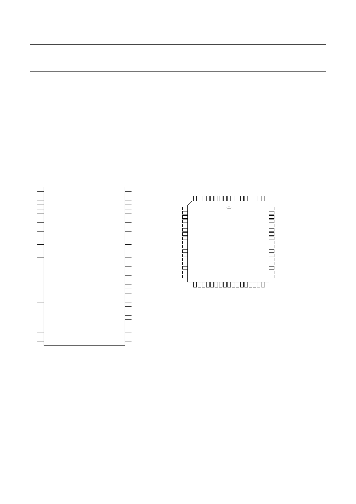
Package Mechanical Drawing . . . . . .. . . . . . . . . . . . . . . . . . . . . . . . . . . . . . . . . . . . . . . . . . . . . . . . . . . . . . . . . . . . . . . . . . . . . . . . . . . .1
. . . . . . . . . . . . . . . . . . . . . . . . . . . . . . . . . . . . . . . . . . . . . . . . . . . . . . . . . . . . . . . . . . . . . . . . . . . . . . . . . . . . . . . . . . . . . . . . . . . . 2
. . . . . . . . . . . . . . . . . . . . . . . . . . . . . . . . . . . . . . . . . . . . . . . . . . . . . . . . . . . . . . . . . . . . . . . . . . . . . . . . . . . . . . . . . . . . . . . . . . 2
SCbus/ST-BUS Mode . . . . . . . . . . . . . . . . . . . . . . . . . . . . . . . . . . . . . . . . . . . . . . . . . . . . . . . . . . . . . . . . . . . . . . . . . . . . . . . . . . . . . . . . . . 2
PEB Mode . . . . . . . . . . . . . . . . . . . . . . . . . . . . . . . . . . . . . . . . . . . . . . . . . . . . . . . . . . . . . . . . . . . . . . . . . . . . . . . . . . . . . . . . . . . . . . . . . . 2
CPU Data Switching. . . . . . . . . . . . . . . . . . . . . . . . . . . . . . . . . . . . . . . . . . . . . . . . . . . . . . . . . . . . . . . . . . . . . . . . . . . . . . . . . . . . . . . . . . . . 2
Internal Bus Data Switching . . . . . . . . . . . . . . . . . . . . . . . . . . . . . . . . . . . . . . . . . . . . . . . . . . . . . . . . . . . . . . . . . . . . . . . . . . . . . . . . . . . . . . . 2
Loopback Mode . . . . . . . . . . . . . . . . . . . . . . . . . . . . . . . . . . . . . . . . . . . . . . . . . . . . . . . . . . . . . . . . . . . . . . . . . . . . . . . . . . . . . . . . . . . . . . . 2
Additional Features . . . . . . . . . . . . . . . . . . . . . . . . . . . . . . . . . . . . . . . . . . . . . . . . . . . . . . . . . . . . . . . . . . . . . . . . . . . . . . . . . . . . . . . . . . . . 3
. . . . . . . . . . . . . . . . . . . . . . . . . . . . . . . . . . . . . . . . . . . . . . . . . . . . . . . . . . . . . . . . . . . . . . . . . . . . . . . . . . . . . . . . . . . . . . . . . . . . . . 3
Logical Pin Organization . .. . . . . . . . . . . . . . . . . . . . . . . . . . . . . . . . . . . . . . . . . . . . . . . . . . . . . . . . . . . . . . . . . . . . . . . . . . . . . . . . . . . . .3
Physical Pinout . . . . . . . . . . . . . . . . . . . . . . . . . . . . . . . . . . . . . . . . . . . . . . . . . . . . . . . . . . . . . . . . . . . . . . . . . . . . . . . . . . . . . . . . . . . . . .3
Pin Description . . . . . . . . . . . . . . . . . . . . . . . . . . . . . . . . . . . . . . . . . . . . . . . . . . . . . . . . . . . . . . . . . . . . . . . . . . . . . . . . . . . . . . . .4
. . . . . . . . . . . . . . . . . . . . . . . . . . . . . . . . . . . . . . . . . . . . . . . . . . . . . . . . . . . . . . . . . . . . . . . . . . . . . . . . . . . . . . . . . . 6
Microprocessor Interface Registers . . . . . . . . . . . . . . . . . . . . . . . . . . . . . . . . . . . . . . . . . . . . . . . . . . . . . . . . . . . . . . . . . . . . . . . . . . . . . . . . . . 6
Command/Status Register . . . . . . . . . . . . . . . . . . . . . . . . . . . . . . . . . . . . . . . . . . . . . . . . . . . . . . . . . . . . . . . . . . . . . . . . . . . . . . 6
Internal Registers . . . . . . . . . . . . . . . . . . . . . . . . . . . . . . . . . . . . . . . . . . . . . . . . . . . . . . . . . . . . . . . . . . . . . . . . . . . . . . . . . . . . . . . . . . . . . . 7
Internal Register Memory Map. . . . . . . . . . . . . . . . . . . . . . . . . . . . . . . . . . . . . . . . . . . . . . . . . . . . . . . . . . . . . . . . . . . . . . . . . . . . . . . . . . 7
Configuration Registers . . . . . . . . . . . . . . . . . . . . . . . . . . . . . . . . . . . . . . . . . . . . . . . . . . . . . . . . . . . . . . . . . . . . . . . . . . . . . . . . . . . . . . . . . 7
Version/Revision Register (O4H) . . . . . . . . . . . . . . . . . . . . . . . . . . . . . . . . . . . . . . . . . . . . . . . . . . . . . . . . . . . . . . . . . . . . . . . . . . . . . . . 10
Destination Routing Memory (80H-9FH) . . . . . . . . . . . . . . . . . . . . . . . . . . . . . . . . . . . . . . . . . . . . . . . . . . . . . . . . . . . . . . . . . . . . . . . . . 10
Source Routing Memory (A0H-BFH) . . . . . . . . . . . . . . . . . . . . . . . . . . . . . . . . . . . . . . . . . . . . . . . . . . . . . . . . . . . . . . . . . . . . . . . . . . . . 11
Destination Parallel Access Registers (C0H-DFH) . . . . . . . . . . . . . . . . . . . . . . . . . . . . . . . . . . . . . . . . . . . . . . . . . . . . . . . . . . . . . . . . . . 12
Source Parallel Access Registers (E0H-FFH). . . . . . . . . . . . . . . . . . . . . . . . . . . . . . . . . . . . . . . . . . . . . . . . . . . . . . . . . . . . . . . . . . . . . . 12
. . . . . . . . . . . . . . . . . . . . . . . . . . . . . . . . . . . . . . . . . . . . . . . . . . . . . . . . . . . . . . . . . . . . . . . . . . . . . . . . . 13
Absolute Maximum Ratings . . . . . . . . . . . . . . . . . . . . . . . . . . . . . . . . . . . . . . . . . . . . . . . . . . . . . . . . . . . . . . . . . . . . . . . . . . . . . . 13
CRecommended DC Operating Conditions . . . . . . . . . . . . . . . . . . . . . . . . . . . . . . . . . . . . . . . . . . . . . . . . . . . . . . . . . . . . . . . . . . . . . . . . . . . 13
DC Electrical Characteristics . . . . . . . . . . . . . . . . . . . . . . . . . . . . . . . . . . . . . . . . . . . . . . . . . . . . . . . . . . . . . . . . . . . . . . . . . . . . . . . 13
. . . . . . . . . . . . . . . . . . . . . . . . . . . . . . . . . . . . . . . . . . . . . . . . . . . . . . . . . . . . . . . . . . . . . . . . . . . . . . . . . . . . . . . . . . . 14
Microprocessor Interface Timing. . . . . . . . . . . . . . . . . . . . . . . . . . . . . . . . . . . . . . . . . . . . . . . . . . . . . . . . . . . . . . . . . . . . . . . . . . . . . .14
Local and Expansion Bus Timing . . . . . . . . . . . . . . . . . . . . . . . . . . . . . . . . . . . . . . . . . . . . . . . . . . . . . . . . . . . . . . . . . . . . . . . . . . . . . .16
Clock and Sync Input Timing . . . . . . . . . . . . . . . . . . . . . . . . . . . . . . . . . . . . . . . . . . . . . . . . . . . . . . . . . . . . . . . . . . . . . . . . . . . . . . .30
2000 Sep 07 2

Philips Semiconductors Preliminary specification
Universal Timeslot Interchange SC2000
FEATURES
• Multi-time slot switching capability
for N x 64K channels (N = 1 to 32).
• Architecture optimized for the call
processing environment: SCSA
TM
PEB
, or MVIPTM compatible.
TM
,
• Two software selectable expansion
bus formats:
• SCbus
TM
/ST-BUS
TM
• PEB
• Two software selectable local bus
formats:
• ST-BUS
• PEB
• Enhanced input hysteresis threshold.
• 32 x 2048 channel switch
• Serial or parallel access to the SCbus.
MC Rx data
MC Tx data
Microprocessor Bus
Clock in
Clock Out
Microprocessor
Interface
SI
SO
Local
Bus
Interface
CLKFAIL&
MC bus
Configuration
registers
Parallel
Access
Registers
Routing
Memory
Switch
Matrix
Timing
Block Diagram
• Internal support for SCbus clock
fallback
• Built-in SCbus message bus
interface
• Supports both Intel® and Motorola®
processor interfaces
• 68-pin PLCC package
• 5v CMOS technology
CLKFAIL
MC
Expansion
Bus
Interface
Expansion Serial Bus
Expansion Clock Out
0.995 [25.27]
0.985 [25.02]
0.056 [1.42]
0.042 [1.07]
0.200 [5.08]
0.165 [4.19]
0.800 [20.32]
REF
0.048 [1.22]
0.042 [1.07]
0.995 [25.27]
0.985 [25.02]
0.800 [20.32] REF
PIN 1
INDEX
0.130 [3.30]
0.090 [2.29]
2000 Sep 07 3
Package Mechanical Drawing

Philips Semiconductors Preliminary specification
Universal Timeslot Interchange SC2000
OVERVIEW
The SC2000 is a custom VLSI circuit
optimized for use in the call processing
environment. The SC2000 provides a
cost-effective means of implementing
the interface between a high speed
internal TDM bus and an external
(expansion) TDM bus. Internal buffering allows the exchange of data between
TDM buses of different speeds and
architectures.
The SC2000 supports two external bus
formats; SCbus/ST-BUS and PEB,
and two internal bus formats; SCbus/
ST-BUS and PEB. It is compatible with
SCSA, PEB, or MVIP requirements.
SCbus operation is also compatible
with the Siemens PCM Highway.
The switching function and operational
configurations of the SC2000 are fully
software programmable. The processor
bus interface is pin configured, allowing
ease of use with a wide variety of industry-standard CPUs.
DESCRIPTION
The primary function of the SC2000 is
to exchange digital data between the
time slot on the local bus and the time
slot on the expansion bus . A microprocessor interface allows the host CPU to
define the time slots and serial streams
between which the data is exchanged.
SCbus/ST-BUS Mode
In SCbus mode the serial streams of the
external bus can be programmed to
operate at 2.048 Mbps, 4.096 Mbps or
8.192 Mbps. The local bus will always
operate at 2.048 Mbps.
The local-to-external bus switch connection is defined by the contents of the
destination routing memory. There are
32 destination routing memory locations, one corresponding to each time
slot of the local bus. The data stored in
the destination routing memory selects
the time slot and serial stream of the expansion bus to which the local bus input
(SI) will be connected.
The external-to-local bus switch connection is defined by the contents of the
source routing memory. There are 32
source routing memory locations, one
corresponding to each time slot of the
local bus. The data stored in the source
routing memory selects the time slot and
serial stream to which the local bus output (SO) will be connected.
Writing data into the routing memories
is synchronized with the SCbus timing
so that routing data is only changed on
frame boundaries.
All serial data is buffered in holding registers. The entire contents of the holding
register are transferred to the output
registers on frame boundaries. This
architecture introduces a constant
one-frame delay through the switch.
This constant delay allows bundled
time slots to be switched.
PEB Mode
In PEB mode the serial streams of the
external bus and the local bus may be
selected to run at either 1.544 Mbps
or 2.048 Mbps.
When PEB mode is selected, one of four
PEB configurations may be used:
1. PEB resource mode, without
switching.
2. PEB network mode, without
switching.
3. PEB resource mode, with switching.
4. PEB network mode, with switching.
When switching is not selected the serial
data is simply buffered between the local
bus and the PEB. This maintains the
data position relative to the multi-frame
sync and allows robbed-bit or CAS
signals to propagate transparently.
When switching is selected the serial
data is transferred between the local and
PEB buses via the switching matrix. The
one-frame delay that occurs requires
that robbed-bit or CAS signals be
handled specially.
The advantages of modes with
switching are:
• Timing delays between the local and
PEB bus are decoupled by the switch
matrix
• The local bus can access all PEB data
lines (SERR, SERT, and L_SERT)
• SO can be set to high impedance
on frame boundaries, allowing a
bi-directional local bus to be
implemented
Non-switching modes are the only configurations that support an interface
to an asynchronous PEB.
CPU Data Switching
In addition to switching local bus serial
data to and from the external bus, the
SC2000 also allows the CPU to write
data directly to the external bus. The
chip provides a frame-sync generated
interrupt which enables a group of
time slots to be accessed from the
same frame.
Internal Bus Data Switching
The Source Routing Memory Local
Connect Enable selects the switching
of data from any SI time slot to any SO
time slot. This operation introduces a
constant two-frame delay, as the data
passes through the switch twice.
Loopback Mode
The SCbus Loopback Mode electrically
isolates the SC2000 from the external
bus but still allows access to the local
bus. This mode is intended for isolating
the board from the external bus while
diagnostic tests are being run. A
CLK_IN source is required for this
mode. The recommended CLK_IN
frequencies are 2.048 MHz, 4.096
MHz, 8.192 MHz, 16.384 MHz, or
32.768 MHz.
2000 Sep 07 4
Philips Semiconductors Preliminary specification
Universal Timeslot Interchange SC2000
Additional Features
The SO output may be set to high impedance on frame boundaries by setting
the Source Routing Memory Switch
Output Enable Bit. This allows outputs
from multiple devices to be connected
to a common line. The SO signal may
also be configured as an open collector
output.
The data sample position of both local
and external buses is selectable between
50% and 75% of the bit width.
Logical and Physical Pinout Diagrams
SC2000
D_7
24
26
D_6
D_5
27
D_4
29
D_3
30
D_2
31
D_1
32
D_0
33
A_1
37
A_0
38
CS*
23
RD*(STRB*)
22
WR*(R/W*)
20
RESET
18
I*(M)
17
50
CLK_IN
52
SYNC_IN
39
SI
54
TXD
PLCC68
(MSYNCT) RSRVD
(L_FSYNCT) SD_1
(L_MSYNCT) SD_2
(R_FSYNCT) SD_12
(R_MSYNCT) SD_13
(CLKT) SCLKX2*
(FSYNCT) SCLK
(SERT) FSYNC*
(SIGT) CLKFAIL
(L_CLKT) SD_0
(L_TSX*) SD_3
(L_SERT) SD_4
(L_SIGT) SD_5
(CLKR) SD_6
(FSYNCR) SD_7
(MSYNCR) SD_8
(SERR) SD_9
(SIGR) SD_10
(R_CLKT) SD_11
(R_TSX*) SD_14
(R_SERT) SD_15
(R_SIGT) MC
SO_CLK
SI_CLK
SO_FS
SI_FS
SO_MS
SI_MS
RXD
INT
35
55
57
58
59
61
62
63
65
66
67
1
3
4
5
7
8
9
11
12
13
15
16
41
40
48
47
46
44
SO
43
53
SD_12
SD_13
SD_14
SD_15
MC
I*
RESET
WR*
RD*
CS*
D_7
D_6
Physical Pinout
SD_9
SD_10
SD_11
10
11
12
13
14
15
16
17
18
19
20
21
22
23
24
25
26
D_3
D_4
D_5
SD_6
SD_7
SD_8
SC2000
68-PIN PLCC
(TOP VIEW)
D_0
D_1
D_2
SD_5
123456789
353433323130292827
INT
SD_1
SD_0
CLKFAIL
SD_2
SD_3
SD_4
S1
S0_CLK
S1_CLK
61626364656667
60
FSYNC*
59
RSRVD
58
SCLK
57
56
SCLKX2*
55
TXD
54
RXD
53
SYNC_IN
52
51
CLK_IN
50
49
SO_FS
48
SI_FS
47
SO_MS
46
45
SI_MS
44
43424140393837
S0
68
36
A_0
A_1
Logical Pin Organization
2000 Sep 07 5

Philips Semiconductors Preliminary specification
PIN DESCRIPTION
Universal Timeslot Interchange SC2000
Pin Name
D_0 - D_7 I/O 33, 32, 31, 30,
A_0, A_1 I 38, 37 Address bus. These inputs select the internal register used by a read or write operation. Normally connected to CPU address lines
CS* I 23 Chip Select. This active low input selects the chip for a read or write operation.
I* I 17 Bus Interface Mode Select. This input selects Intel- and Motorola-type data bus interface configurations.
RD*
or
STRB*
WR*
or
R/W*
RESET I 18 Reset.
CLK_IN I 50 Local clock input.
SYNC_IN I 52 Local sync input.
SI I 39 Serial input.
SO O 43 Serial output.
TXD I 54 Transmit data
INT O 35 Interrupt Request.
SCLKx2* or
CLKT
SCLK or
FSYNCT
RSRVD or
MSYNCT
FSYNC* or
SERT
CLKFAIL I/O 61 Register bit C_4 = 0.
SD_0 or
L_CLKT
SD_1 or
L_FSYNCT
SD_2 or
L_MSYNCT
SD_3 or
L_TSX*
Input/Output Pin Number Pin Description
29, 27, 26, 24
I
22 I* = 0. Read
I
I
20 I* = 0. Write
I
I/O
55 Register bit C_4 = 0. SCbus System clock x 2.
I
I/O
57 Register bit C_4 = 0. SCbus System clock.
I
I
58 Register bit C_4 = 0. SCbus Reserved.
I
I/O
59 Register bit C_4 = 0. SCbus Frame sync.
I
I/O
62 Register bit C_4 = 0. SCbus Serial data stream 0.
I/O
I/O
63 Register bit C_4 = 0. SCbus Serial data stream 1.
I/O
I/O
65 Register bit C_4 = 0. SCbus Serial data stream 2.
I/O
I/O
66 Register bit C_4 = 0. SCbus Serial data stream 3.
I/O
Data bus.
These bi-directional, tri-state lines are the SC2000s interface to the CPU data bus.
A0 and A1 in 8-bit CPU systems, or A1 and A2 in 16-bit CPU systems.
0 = Intel. 1 = Motorola.
This active low input enables the data bus drivers to drive the CPU data bus with the contents of the internal register selected by
A_0 and A_1.
I* = 1. Strobe
During a read operation a low on this input enables the data bus drivers to drive the CPU data bus with the contents of the internal
register selected by A_0 and A_1. During a write operation data is transferred from the CPU data bus to the register selected by
A_0 and A_1 on a low to high transition of this signal.
During a write operation data is transferred from the CPU data bus to the register selected by A_0 and A_1 on a low to high
transition of this signal.
I* = 1. Read/Write
This input selects between a write operation (R/W* = 0) and a read operation (R/W* =1).
This active high input forces all outputs to tri-state, and resets the SC2000 chip.
Local serial bus data input line.
Local serial bus data output line.
SCbus Message Bus transmit data input line.
Active high interrupt request output line.
Register bit C_4 = 1. PEB Transmit clock.
Register bit C_4 = 1. PEB Frame sync.
Register bit C_4 = 1. PEB Transmit multi-frame sync.
Register bit C_4 = 1. PEB Transmit serial data.
SCbus Clock fail signal.
Register bit C_4 = 1. PEB Local resource transmit clock.
Register bit C_4 = 1. PEB Local resource transmit frame sync.
Register bit C_4 = 1. PEB Local resource multi-frame sync.
Register bit C_4 = 1. PEB Local resource transmit time slot enable.
2000 Sep 07 6

Philips Semiconductors Preliminary specification
PIN DESCRIPTION (continued)
Universal Timeslot Interchange SC2000
Pin Name Input/Output Pin Number Pin Description
SD_4 or
L_SERT
SD_5 I/O 1 Register bit C_4 = 0.
SD_6 or
CLKR
SD_7 or
FSYNCR
SD_8 or
MSYNCR
SD_9 or
SERR
SD_10 I/O 8 Register bit C_4 = 0.
SD_11 I/O 9 Register bit C_4 = 0.
SD_12 I/O 11 Register bit C_4 = 0.
SD_13 I/O 12 Register bit C_4 = 0.
SD_14 I/O 13 Register bit C_4 = 0.
SD_15 I/O 15 Register bit C_4 = 0.
MC I/O 16 Register bit C_4 = 0.
SO_CLK O 41 Serial Output Clock.
SI_CLK O 40 Serial Input Clock.
SO_FS O 48 Serial Output Frame Sync.
SI_FS O 47 Serial Input Frame Sync.
SO_MS O 46 Serial Output Multi-frame Sync.
SI_MS O 44 Serial Input Multi-frame Sync.
RXD O 53 Receive Data. Message channel serial data output.
VDDO1 -
VDDO5
VDDI1 -
VDDI3
VSSO1 -
VSSO7
VSSI1 -
VSSI3
I/O
I/O
I/O
I/O
I/O
I/O
I/O
I/O
I/O
I/O
Power 2, 10, 25, 45, 60 I/O pad VDD (+5 V).
Power 19, 34, 51 Core V
Power 6, 14, 28, 42, 56,
Power 21, 36, 49 Core VSS (GND).
67 Register bit C_4 = 0. SCbus Serial data stream 4.
3 Register bit C_4 = 0. SCbus Serial data stream 6.
4 Register bit C_4 = 0. SCbus Serial data stream 7.
5 Register bit C_4 = 0. SCbus Serial data stream 8.
7 Register bit C_4 = 0. SCbus Serial data stream 9.
64, 68
Register bit C_4 = 1. PEB Local resource transmit serial data.
SCbus Serial data stream 5.
Register bit C_4 = 1. PEB Receive clock.
Register bit C_4 = 1. PEB Receive frame sync.
Register bit C_4 = 1. PEB Receive multi-frame sync.
Register bit C_4 = 1. PEB Receive data stream.
SCbus Serial data stream 10.
SCbus Serial data stream 11.
SCbus Serial data stream 12.
SCbus Serial data stream 13.
SCbus Serial data stream 14.
SCbus Serial data stream 15.
SCbus Message Bus signal.
Clock for local serial output data.
Clock for local serial input data.
Frame sync for local serial output data.
Frame sync for local serial input data.
Multi-frame sync for local serial output data.
Multi-frame sync for local serial input data.
(+5 V).
DD
I/O pad VSS (GND).
2000 Sep 07 7

Philips Semiconductors Preliminary specification
Universal Timeslot Interchange SC2000
REGISTER DESCRIPTION
Microprocessor Interface Registers
The four 8-bit Microprocessor Interface
Registers comprise the command and
control port for the SC2000.
Command/Status Register
Busy (CS_0): This bit is automatically
set to 1 when a command that requires
synchronization with the SC2000’s internal state machine has been initiated.
The bit is cleared to 0 when the command has been completed. The following commands require synchronization:
• Destination Routing Memory Write
• Source Routing Memory Write
• Parallel Access Destination Write
• Parallel Access Source Read
Read (CS_1): Setting this bit to 1 ini-
tiates a read of the register pointed to
by the contents of the Internal Address
Register. Once the BUSY bit is read as
cleared to 0 the contents of the selected
register will be available in the Low Byte
and High Byte Data Registers. Once the
READ operation is complete the READ
bit is cleared automatically.
Write (CS_2):
tiates a write to the register pointed to
by the contents of the Internal Address
Register. Once the busy bit has been
cleared to 0 the contents of the Low Byte
and High Byte Data Registers have been
transferred into the selected register.
Once the WRITE operation is completed the WRITE bit is cleared automatically.
Setting this bit to 1 ini-
Terminate (CS_3): Setting this bit to 1
terminates any command that requires
synchronization with the SC2000’s internal state machine. This command is
needed to complete a command when
the SC2000’s internal state machine has
stopped running due to the failure of the
system clocks. The command currently
being executed is completed asynchronously and the BUSY bit is cleared to 0.
To restore normal operation the TERMINATE bit must be explicitly cleared
to 0. This bit can be read back for verification purposes.
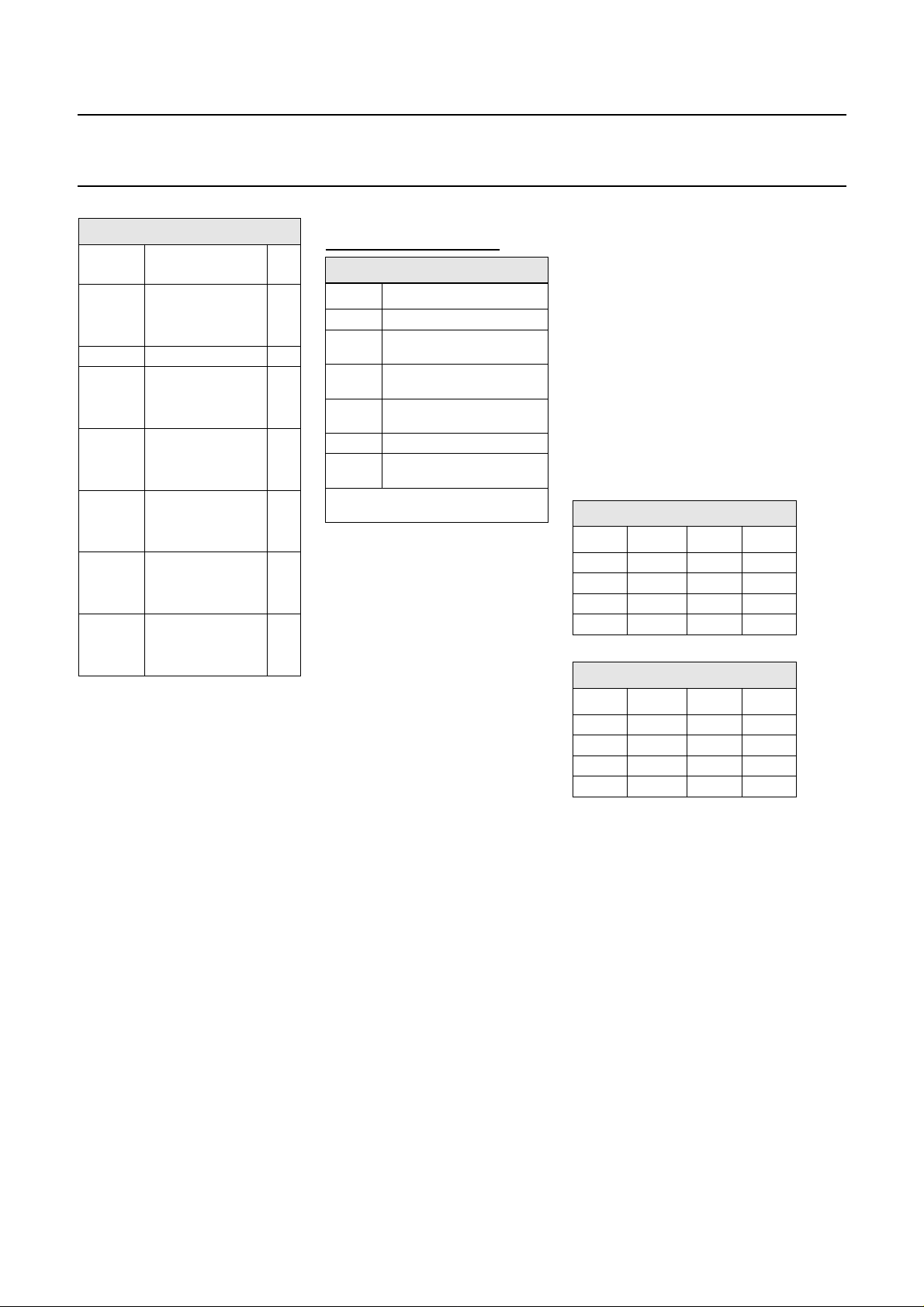
Command/Status Register
BIT R/W Command/Status
0 R CS_0: Busy (S)
1 W CS_1: Read (C)
2 W CS_2: Write (C)
3 R/W CS_3: Terminates (C)
4 CS_4: Reserved
5 CS_5: Reserved
6 CS_6: Reserved
7 R/W CS_7: Reset (C)
Note: (1) Bit 0 is the LSB of the byte.
(2) Initiating multiple commands in a
single access is not recommended.
CPU Interface Register Map
A_1 A_0 Register Name
0 0 Command/Status
0 1 Internal Address
1 0 Low Byte Data
1 1 High Byte Data
Low Byte Data Register
BIT R/W Function
0 R/W D_0
1 R/W D_1
2 R/W D_2
3 R/W D_3
4 R/W D_4
5 R/W D_5
6 R/W D_6
7 R/W D_7
Note: Bit 0 is the LSB of the byte.
High Byte Data Register
BIT R/W Function
0 R/W D_8
1 R/W D_9
2 R/W D_10
3 R/W D_11
4 R/W D_12
5 R/W D_13
6 R/W D_14
7 R/W D_15
Note: Bit 0 is the LSB of the byte.
2000 Sep 07 8
Philips Semiconductors Preliminary specification
Universal Timeslot Interchange SC2000
Internal Register Memory Map
Values for
A_7 .. A_0 (H)
00
.
.
03
04 Version/Revision R/W
05
.
.
7F
80
.
.
9F
A0
.
.
BF
C0
.
.
DF
E0
.
.
FF
Function R/W
Configuration 1
.
.
Configuration 4
Reserved
.
.
Reserved
Destn Routing
.
.
Destn Routing
Source Routing
.
.
Source Routing
Destn Parallel
.
.
Destn Parallel
Source Parallel
.
.
Source Parallel
R/W
R/W
R/W
R/W
R/W
R/W
Reset (CS_7): Setting this bit to 1 forces
the SC2000 into its reset state, and
initializes all internal registers. This
command reproduces the function
of the RESET pin. Setting this bit to 0
returns the SC2000 to normal operation.
This bit can be read back for verification
purposes.
Internal Registers
The internal registers are accessed by
reads and writes to the Data Registers
using the address held in the Internal
Address Register.
Configuration Registers
Configuration Register 1(00H)
Configuration Register 1
BIT Function
0 C_0: Global Output Enable
1 C_1: Expansion Bus Timing
2
3
4 C_4: Expansion Bus
5 C_5: SCbus Loopback Mode
6
7
Note: Bit 0 is the LSB of the Low Byte
Driver Enable
C_2: Framing Mode 0
C_3:Framing Mode 1
Interface Select
C_6: PEB module Type 0
C_7:PEB Module Type 1
Data Register.
Global Output Enable (C_0): Clearing
this bit to 0 forces all outputs to the high
impedance state, with the exception of
the microprocessor interface data bus.
Setting this bit to 1 enables all outputs.
This bit is cleared on RESET.
Expansion Bus Timing Driver
Enable (C_1): When SCbus Mode is
selected (C_4 = 0), clearing this bit to
0 disables the expansion bus timing
drivers.
When PEB Resource Mode is selected
(C_6, C_4 = 01), this bit has no effect.
When PEB Network Mode is selected
(C_6, C_4 = 11), clearing this bit to 0
disables the expansion bus drivers
CLKR, L_CLKT, FSYNCR, L_FSYNCT,
MSYNCR, and L_MSYNCT. Setting this
bit to 1 enables these timing drivers.
This bit is cleared on RESET.
Framing Mode (C_3, C_2): This two-bit
field selects the number of bits per frame
(B/F), time slots per frame (TS/F) and
frames per multi-frame (F/MF) on both
the local and expansion bus.
When SCbus Mode is selected
(C_4 = 0), there is no multi-frame sync
signal available on the expansion bus.
The (00) combination of (C_3, C_2)
is invalid. In this case the internal
multi-frame sync will be free running,
and synchronous to FSYNC.
When PEB Mode is selected (C_4 = 1)
the only valid combinations of (C_3,
C_2) are (00) and (01).
These bits are cleared on RESET.
Expansion Bus
C_3, C_2 B/F TS/F F/MF
00 193 24 12
01 256 32 16
10 512 64 16
11 1024 128 16
Local Bus
C_3, C_2 B/F TS/F F/MF
00 193 24 12
01 256 32 16
10 256 32 16
11 256 32 16
Expansion Bus Interface Select (C_4):
This bit selects the expansion bus interface operating mode. Clearing this bit to
0 selects SCbus Mode. Setting this bit to
1 selects PEB Mode.
This bit is cleared on RESET.
2000 Sep 07 9
Philips Semiconductors Preliminary specification
Universal Timeslot Interchange SC2000
SCbus Loopback Mode Select (C_5):
When SCbus Mode is selected (C_4 =
0), this bit controls the SCbus loopback.
Clearing this bit to 0 disables Loopback
Mode. Setting this bit to 1 enables Loopback Mode.
When PEB Mode is selected (C_4 = 1)
this bit has no effect.
When loopback is enabled the expansion bus timing and data bus drivers are
forced to high impedance, and the data
outputs are looped back internally to the
corresponding inputs. This mode is used
to test the SC2000 without disrupting
the operation of the SCbus.
A clock must be supplied at CLK_IN
for operation in Loopback Mode.
This bit is cleared on RESET.
PEB Module Type (C_7, C_6): When
PEB Mode is selected (C_4 = 1) this
two-bit field selects the PEB module
type.
When SCbus Mode is selected (C_4 = 0)
these bits have no effect.
These bits are cleared on RESET.
PEB Module Type
C_7, C_6 Operating Mode
00 Resource module without switching
01 Network module without switching
10 Resource module with switching
11 Network module with switching
Configuration Register 2 (01H)
Configuration Register 2
Bit Function
0
C_8: CLK_IN Divider 0
1
C_9: CLK_IN Divider 1
2
C_10: CLK_IN Divider 2
3 C_11: SYNC_IN Format
4
C_12: SYNC_IN Select 0
5
C_13: SYNC_IN Select 1
6
C_14: PEB Network
7
Note: Bit 0 is the LSB of the Low Byte
Modul Timing Select 0
C_15: PEB Network
Modul Timing Select 1
Data Register.
CLK_IN Divider (C_10, C_9, C_8):
This field selects the CLK_IN division
ratio used in the generation of the system source clock.
When “CLK_IN divide by 1” and SCbus
Mode are selected and the expansion
bus timing drivers are enabled (C_10,
C_9, C_8, C_4, C_1 = 00001), then
SCLKx2* is held high and the FSYNC*
period is equal to 1 SCLK period.
These bits are cleared on RESET.
CLK_IN Divider
C_10, C_9, C_8 CLK_IN Divided By
000 1
001 2
010 4
011 8
100 16
101 Reserved
110 Reserved
111 Reserved
SYNC_IN Format (C_11): This bit
selects the SYNC_IN format to be either
PEB conventional or ST-BUS. If this bit
is cleared to 0 then SYNC_IN is taken to
be in the PEB conventional format. If
this bit is set to 1, SYNC_IN is taken to
be in the ST-BUS format.
In ST-BUS format the CLK_IN signal is
inverted to produce the system clock
source.
This bit is cleared on RESET.
SYNC_IN Select (C_13, C_12): This
two bit field selects the function of
the SYNC_IN input.
These bits are cleared on RESET.
SYNC_IN Select
C_13, C_12 SYNC_IN Function
00 Ignored
01 Frame sync
10 Ignored
11 Multi-frame sync
PEB Network Module Timing Select
(C_15, C_14): When PEB Network
Module Mode is selected (C_6, C_4,
C_1 = 111), this two bit field selects the
module timing mode.
Otherwise these bits have no effect.
These bits are cleared on RESET.
PEB Network Module Timing Mode
C_15, C_14 Timing Mode
00 Master
01 Master, MSYNCT fi
10 Slave, MSYNCT fi
11 Slave, SYNC_IN fi
L_MSYNCT
MSYNCR
MSYNCR
Configuration Register 3 (02H)
Configuration Register 3
Bit Function
0 C_16: Expansion Bus Data
1 C_17: Local Bus Data
2 C_18: SCbus Output Driver
3 C_19: SO Output Driver
4 C_20: Local Bus Framing Format
5 C_21: Message Channel
6
7
Note: Bit 0 is the LSB of the Low Byte
Sample Position
Sample Position
TXD Select
C_22: SERT Mux 0
C_23: SERT Mux 1
Data Register.
2000 Sep 07 10

Philips Semiconductors Preliminary specification
Universal Timeslot Interchange SC2000
Expansion Bus Data Sample
Position (C_16): When SCbus Mode is
selected (C_4 = 0) this bit determines
the location of the sampled point in the
bit cell. When this bit is cleared to 0,
sampling occurs at 50% of the bit width.
When this bit is set to 1, sampling occurs
at 75% of the bit width.
When PEB Mode is selected (C_4 = 1)
this bit has no effect, and data is always
sampled at the 50% point.
SCLKx2* must be present in order to
sample at the 75% point.
This bit is cleared on RESET.
Local Bus Data Sample Position
(C_17): When SCbus Mode is selected
(C_4 = 0) this bit determines the location of the sample point in the bit cell.
When this bit is cleared to 0 sampling
occurs at 50% of the bit width. When
this bit is set to 1, sampling occurs at
75% of the bit width.
When PEB Mode is selected (C_4 = 1)
this bit has no effect, and data is always
sampled at the 50% point.
SCLKx2* must be present in order to
sample at the 75% point.
This bit is cleared on RESET.
SCbus Output Driver (C_18): When
SCbus Mode is selected (C_4 = 0), this
bit determines the SCbus output driver
type. When this bit is cleared to 0, the
output drivers are configured as tri-state
type. When this bit is set to 1 the output
drivers are configured as open collector
type.
When PEB Mode is selected (C_4 = 1)
this bit has no effect. PEB outputs are
always driven open collector.
All SCbus outputs are affected by this bit
with the exception of CLKFAIL and MC,
which are always driven open collector.
This bit is cleared on RESET.
SO Output Driver (C_19): This bit
determines the SO output driver type.
When this bit is cleared to 0 the output
drivers are configured as tri-state. When
this bit is set to 1 the output drivers are
configured as open collector.
When PEB Mode without switching
is selected (C_7, C_4 = 01) then SO is
always enabled.
This bit is cleared on RESET.
Local Bus Framing Format (C_20):
When SCbus Mode is selected
(C_4 = 0) this bit determines the local
bus framing format. When this bit is
cleared to 0 the local bus operates with
PEB conventional framing format.
When this bit is set to 1 the local bus operates with ST-BUS framing format.
When PEB Mode is selected (C_4 = 1)
this bit has no effect.
With ST-BUS framing format selected,
SI_CLK is replaced by C4*, SI_FS by
F0*, and SI_MS by M0*. SO_CLK,
SO_FS and SO_MS are unaffected by
the status of this bit, and continue to
output PEB conventional framing.
ST-BUS Framing Format Replacements
PEB Conventional ST-BUS
SI_CLK C4*
SI_FS F0*
SI_MS M0*
SCLKx2* must be present, or SCLK
must be at least twice the local clock
(CLK_IN) frequency for ST-BUS framing format to be used.
This bit is cleared on RESET.
Message Channel TXD Select (C_21):
When SCbus Mode is selected
(C_4 = 0) this bit determines the
configuration of the TXD input. When
this bit is cleared to 0, the TXD input
is configured as a transparent buffer.
When this bit is set to 1 the TXD input
is configured as a latched buffer.
When PEB Mode is selected (C_4 = 1),
this bit has no effect. MC is not used in
PEB mode.
When a transparent buffer is selected
(C_21 = 0), the HDLC controller should
output TXD on the rising edge of
SO_CLK. When a latched buffer is
selected (C_21 = 1) the HDLC controller should output TXD on the falling
edge of SO_CLK.
This bit is cleared on RESET.
SERT Mux (C_23, C_22): When PEB
Network Mode is selected, this two bit
field selects the source of data for the local bus SO serial stream.
When SCbus Mode (C_7, C_6,
C_4 = xx0) or PEB Resource Mode
(C_7, C_6, C_4 = 001) are selected,
these bits have no effect.
PEB Data Source Stream
C_23, C_22 Data Source
00 L_SERT
01 (L_SERT* !L_TSX*)
+(SERT* L_TSX*)
Configuration Register 4 (03H)
Configuration Register 4
Bit Function
0 C_24: CLKFAIL latch
1 C_25: CFSYNC latch
2 C_26: CLKFAIL latch Clear*
3 C_27: FSYNC latch Clear*
4 C_28: CLKFAIL polarity
5 C_29: INT Mask*
6 C_30: INT polarity
7 C_31: INT ouput driver
Note: Bit 0 is the LSB of the Low Byte
Data Register.
CLKFAIL Latch (C_24): When SCbus
Mode is selected (C_4 = 0) this bit indicates the status of the CLKFAIL latch.
0 →
CLKFAIL clear
1 → CLKFAIL set
When PEB Mode is selected (C_4 = 1),
this bit is always clear.
2000 Sep 07 11

Philips Semiconductors Preliminary specification
Universal Timeslot Interchange SC2000
FSYNC Latch (C_25): When SCbus
Mode (C_4 = 0) or PEB Mode with
switching (C_7, C_4 = 11) are selected,
these bits indicate the status of the
FSYNC latch.
0 → FSYNC clear
1 → FSYNC set
When a PEB Mode without switching
is selected (C_7, C_4 = 01) this bit is
always clear.
CLKFAIL Latch Clear* (C_26): This bit
resets the CLKFAIL latch. Clearing this
bit to 0 clears the CLKFAIL latch and
disables CLKFAIL interrupts. Setting
this bit to 1 enables CLKFAIL interrupts.
This bit is cleared on RESET.
FSYNC Latch Clear* (C_27): This bit
resets the FSYNC latch. Clearing this bit
to 0 clears the FSYNC latch and disables
FSYNC interrupts. Setting this bit to 1
enables FSYNC interrupts.
This bit is cleared on RESET.
CLKFAIL Polarity (C_28): This bit
controls the level of the CLKFAIL signal
which will set the CLKFAIL latch. When
this bit is cleared to 0, the CLKFAIL
latch is set when the CLKFAIL signal is
“lo” (0). When this bit is set to 1 the
CLKFAIL latch is set when the CLKFAIL
signal is “hi” (1).
The “CLKFAIL = 0” interrupt mode is
used by the new clock master to determine that clock fall back has been executed effectively. The “CLKFAIL = 1”
interrupt mode is used by the standby
clock board to detect clock failure.
This bit should only be changed when
the CLKFAIL interrupt is disabled
(C_26 = 0).
This bit is cleared on RESET.
INT Mask* (C_29): This bit controls the
interrupts generated by CLKFAIL and
FSYNC (INT = CLKFAIL + FSYNC).
When this bit is cleared to 0 all interrupts are masked. When this bit is set
to 1, interrupts are enabled.
The status of this bit does not affect the
CLKFAIL Latch or FSYNC Latch bits
(C_24 and C_25), and these bits can still
be used to determine the status of the
two latches.
This bit is cleared on RESET.
INT Output Polarity (C_30): This bit
controls the active level of the INT interrupt output. When this bit is cleared
to 0, then the INT output is active low.
When this bit is set to 1 then the INT
output is active high.
This bit is cleared on RESET.
INT Output Driver (C_31): This bit
controls the configuration of the INT
output driver. When this bit is cleared to
0, the INT output driver is configured as
open collector. When this bit is set to 1
the INT output driver is configured as
totem-pole.
Version/Revision Register (04H): The
Version/Revision Register is an 8-bit
read-only register used to identify the
version and revision status of a particular batch of SC2000s. It is recommended
that a test of this field be included in all
firmware interface code to ensure compatibility.
Version/Revision Register 1
BIT Function
0 Rev 0
1 Rev 1
2 Rev 2
3 Rev 3
4 Ver 0
5 Ver 1
6 Ver 2
7 Ver 3
Note: Bit 0 is the LSB of the Low Byte
Data Register.
The initial release of the SC2000 will be
Version/Revision = 00H.
Destination Routing Memory
(80H - 9FH): The Destination Routing
Memory maps time slots from the local
SI bus onto the expansion bus. Each
location in the Destination Routing
Memory corresponds to a time slot
on the local SI bus. The contents of
each location specify a time slot on
the expansion bus.
Destination Routing Memory Map
IAR Destination Map
80H Channel 0
81H Channel 1
82H Channel 2
.
.
.
.
9FH Channel 31
Note: IAR = Internal Address register contents.
Channel N is equivalent to time slot N
on the local SI bus.
The contents of all Destination Routing
Memory Locations are cleared on RESET.
When writing data into the Destination
Routing Memory the Low Byte Data
Register contains a 7-bit binary field
holding a time slot number, and the
High Data Byte Register contains a 4-bit
binary field holding a Port (stream)
number. Together these two fields
uniquely identify a time slot on the
expansion bus which will be the destination for data from the local SI bus.
2000 Sep 07 12

Philips Semiconductors Preliminary specification
Universal Timeslot Interchange SC2000
Time Slot Select (DR_6 .. DR_0): This
7-bit field specifies a time slot number
between 0 and 127. DR_6 is the MSB of
this field.
Destination Routing Memory LSB
Bit Function
0
DR_0: Time slot Select 0
1
DR_1: Time slot Select 1
2
DR_2: Time slot Select 2
3
DR_3: Time slot Select 3
4
DR_4: Time slot Select 4
5
DR_5: Time slot Select 5
6
DR_6: Time slot Select 6
7 DR_7: Reserved
Note: Bit 0 is the LSB of the Low Byte
Data Register.
Port Select (DR_11 .. DR_8): When
SCbus mode is selected (C_4 = 0) this
4-bit field specifies an SCbus data
stream number between 0 and 15.
DR_11 is the MSB of this field.
When a PEB Mode with switching is
selected (C_6, C_4 = 11) this 4- bit field
specifies a PEB data stream. See table for
details.
Destination Routing Memory MSB
Bit Function
0
DR_8: Port Select 0
1
DR_9: Port Select 1
2
DR_10: Port Select 2
3
DR_11: Port Select 3
4 DR_12: Reserved
5 DR_13: Reserved
6 DR_14: Parallel Access Enable
7 DR_15: Switch Output Enable
Note: Bit 0 is the LSB of the High Byte
Data Register.
Destination Port Select (PEB Mode)
DR_11..DR_8 PEB Destination
0H L_SERT/L_TSX*
1H SERR
2H R_SERT/R_TSX*
3H SERT
4H
Reserved
.
.
.
.
FH
Reserved
Parallel Access Enable (DR_14): When
this bit is cleared to 0, the SC2000 uses
the local SI bus as the source of data
for the expansion bus. When this bit is
set to 1 the SC2000 uses the contents of
the corresponding Destination Parallel
Access Register as the source of expansion bus data.
Switch Output Enable (DR_15): When
this bit is cleared to 0, the SC2000 expansion bus drivers are forced to the
high impedance state during the specified time slot period. When this bit is set
to 1 the SC2000 expansion bus drivers
drive the bus during the specified time
slot period.
Source Routing Memory (A0H - BFH):
The Source Routing Memory maps time
slots from the expansion bus onto time
slots on the local SO bus. Each location
in the Source Routing Memory
corresponds to a time slot on the
local SO bus.
Source Routing Memory
IAR Source Mapping
A0H Channel 0
A1H Channel 1
A2H Channel 2
.
.
.
.
BFH Channel 31
Note: IAR = Internal Address register contents.
Channel N is equivalent to time slot N
on the local S0 bus.
The contents of all Source Routing
Memory Location are cleared on
RESET.
When writing data into the Source
Routing Memory the Low Byte Data
Register contains a 7-bit binary field
holding a time slot number, and the
High Data Byte Register contains a 4-bit
binary field holding a Port (stream)
number. Together these two fields
uniquely identify a time slot on the
expansion bus which will be used as a
source of data for a time slot on the local
SO bus.
Time slot Select (SR_6 .. SR_0): This
7-bit field specifies a time slot number
between 0 and 127. SR_6 is the MSB of
this field.
Source Routing Memory LSB
Bit Function
0
SR_0: Time Slot Select 0
1
SR_1: Time Slot Select 1
2
SR_2: Time Slot Select 2
3
SR_3: Time Slot Select 3
4
SR_4: Time Slot Select 4
5
SR_5: Time Slot Select 5
6
SR_6: Time Slot Select 6
7 SR_7: Reserved
Note: Bit 0 is the LSB of the Low Byte
Data Register.
Port Select (SR_11 .. SR_8): When
SCbus Mode is selected (C_4 = 0),
this 4-bit field specifies an SCbus data
stream number between 0 and 15.
SR_11 is the MSB of this field.
When a PEB Mode with switching is
selected (C_6, C_4 = 11) this 4-bit field
specifies a PEB data stream as follows:
2000 Sep 07 13

Philips Semiconductors Preliminary specification
Universal Timeslot Interchange SC2000
SR_11 is the MSB of this field.
Source Routing Memory MSB
Bit Function
0
SR_8: Port Select 0
1
SR_9: Port Select 1
2
SR_10: Port Select 2
3
SR_11: Port Select 3
4 SR_12: Reserved
5 SR_13: Reserved
6 SR_14: Local Connect Enable
7 SR_15: Switch Output Enable
Note: Bit 0 is the LSB of the High Byte
SR_11..SR_8 Source PEB Stream
Data Register.
PEB Mode Source Data Stream
0H SERT Mux
1H SERR
2H R_SERT
3H SERT
4H
FH
Reserved
.
.
.
.
Reserved
Local Connect Enable (SR_14): This bit
controls the internal connection time
slots on the local bus. When this bit is
cleared to 0 Local Connect is disabled.
When this bit is set to 1 Local Connect is
enabled and a time slot on the local SI
bus will be connected internally to a
time slot on the local SO bus.
When Local Connect is enabled the
Source Routing Memory Time slot
Select bits (SR_0 .. SR_6) select the
destination time slot on the local SO
bus. The contents of the Port Select
field (SR_8 .. SR_11) are ignored.
Switch Output Enable (SR_15): When
this bit is cleared to 0 the local SO bus
drivers are forced to the high impedance
state during the specified time slot period. When this bit is set to 1 the local
SO bus drivers drive the bus during the
specified time slot period.
Destination Parallel Access Registers
(C0H .. DFH): If Parallel Access and
Switch Output are enabled, the device
CPU can write data to the expansion bus
via these SC2000 registers. The write
mapping is controlled by the Destination Routing Memory. The contents of
the selected Parallel Access Register will
replace the contents of the local SI bus
time slot that would otherwise have
been transferred to the expansion bus.
Destination Parallel Access Regs
IAR SI Destination
C0H Channel 0
C1H Channel 1
C2H Channel 2
.
.
.
.
DFH Channel 31
Note: IAR = Internal Address Register con-
tents. Channel N is equivalent to time
slot N on the local SI bus.
Source Parallel Access Registers
( E0H .. FFH): The Source Parallel
Access Registers are continually loaded
with the data being written to the corresponding local SO bus time slot, irrespective of the status of the Parallel
Access Enable or Switch Output Enable
bits. If Local Connect is enabled this
data will originate from the local SI bus.
Source Parallel Access Regs
IAR SO Destination
E0H Channel 0
E1H Channel 1
E2H Channel 2
.
.
.
.
FFH Channel 31
Note: IAR = Internal Address Register con-
tents. Channel N is equivalent to time
slot N on the local SO bus.
2000 Sep 07 14
 Loading...