

INTEGRATED CIRCUITS
DATA SH EET
SAF7113H
9-bit video input processor
Product specification
File under Integrated Circuits, IC22
2000 May 08

Philips Semiconductors Product specification
9-bit video input processor SAF7113H
CONTENTS
1 FEATURES
2 APPLICATIONS
3 GENERAL DESCRIPTION
4 QUICK REFERENCE DATA
5 ORDERING INFORMATION
6 BLOCK DIAGRAM
7 PINNING
8 FUNCTIONAL DESCRIPTION
8.1 Analog input processing
8.2 Analog control circuits
8.3 Chrominance processing
8.4 Luminance processing
8.5 Synchronization
8.6 Clock generation circuit
8.7 Power-on reset and CE input
8.8 Multi-standard VBI data slicer
8.9 VBI-raw data bypass
8.10 Digital output port VPO7 to VPO0
8.11 RTCO output
8.12 RTS0, RTS1 terminals
9 BOUNDARY SCAN TEST
9.1 Initialization of boundary scan circuit
9.2 Device identification codes
10 LIMITING VALUES
11 THERMAL CHARACTERISTICS
12 CHARACTERISTICS
13 TIMING DIAGRAMS
13.1 Errata information
14 APPLICATION INFORMATION
15 I2C-BUS DESCRIPTION
15.1 I2C-bus format
15.2 I2C-bus detail
16 I2C-BUS START SET-UP
17 PACKAGE OUTLINE
18 SOLDERING
18.1 Introduction to soldering surface mount
packages
18.2 Reflow soldering
18.3 Wave soldering
18.4 Manual soldering
18.5 Suitability of surface mount IC packages for
wave and reflow soldering methods
19 DATA SHEET STATUS
20 DEFINITIONS
21 DISCLAIMERS
22 PURCHASE OF PHILIPS I2C COMPONENTS
2000 May 08 2

Philips Semiconductors Product specification
9-bit video input processor SAF7113H
1 FEATURES
• Four analog inputs, internal analog source selectors,
e.g. 4 × CVBS or 2 × Y/C or (1 × Y/C and 2 × CVBS)
• Two analog preprocessing channels in differential
CMOS style for best S/N-performance
• Fullyprogrammablestaticgainorautomaticgaincontrol
for the selected CVBS or Y/C channel
• Switchable white peak control
• Two built-in analog anti-aliasing filters
• Two 9-bit video CMOS Analog-to-Digital Converters
(ADCs), digitized CVBS or Y/C-signals are available on
the VPO-port via I2C-bus control
• On-chip clock generator
• Line-locked system clock frequencies
• Digital PLL for horizontal sync processing and clock
generation, horizontal and vertical sync detection
• Requires only one crystal (24.576 MHz) for all standards
• Automatic detection of 50 and 60 Hz field frequency,
and automatic switching between PAL and NTSC
standards
• Luminance and chrominance signal processing for
PAL BGHI, PAL N, combination PAL N, PAL M,
NTSC M, NTSC N, NTSC 4.43, NTSC-Japan and
SECAM
• User programmable luminance peaking or aperture
correction
• Cross-colour reduction for NTSC by chrominance comb
filtering
• PAL delay line for correcting PAL phase errors
• Brightness Contrast Saturation (BCS) and hue control
on-chip
• Real-time status information output (RTCO)
• Two multi functional real-time output pins controlled by
I2C-bus
• Multi-standardVBI-dataslicerdecodingWorld Standard
Teletext (WST), North-American Broadcast Text
System (NABTS), closed caption, Wide Screen
Signalling (WSS), Video Programming System (VPS),
Vertical Interval Time Code (VITC) variants
(EBU/SMPTE) etc.
• Standard ITU 656 YUV4:2:2 format (8-bit) on VPO
output bus
• Enhanced ITU 656 output format on VPO output bus
containing:
– active video
– raw CVBS data for INTERCAST applications
(27 MHz data rate)
– decoded VBI data
• Boundary scan test circuit complies with the
1149.b1 - 1994”
• I2C-bus controlled (full read-back ability by an external
controller, bit rate up to 400 kbits/s)
• Lowpower (<0.5 W), low voltage (3.3 V), small package
(QFP44)
• Power saving mode by chip enable input
• Detection of copy protected input signals according to
the macrovision standard. Can be used to prevent
unauthorized recording of pay-TV or video tape signals.
2 APPLICATIONS
• Notebook (low power consumption)
• PCMCIA card application
• AGP based graphics cards
• Image processing
• Video phone applications
• Intercast and PC teletext applications
• Security applications.
(ID-Code = 1 7113 02B)
“IEEE Std.
2000 May 08 3

Philips Semiconductors Product specification
9-bit video input processor SAF7113H
3 GENERAL DESCRIPTION
The 9-bit video input processor is a combination of a
two-channel analog preprocessing circuit including source
selection, anti-aliasing filter and ADC, an automatic clamp
and gain control, a Clock Generation Circuit (CGC), a
digitalmulti-standard decoder (PAL BGHI, PAL M, PAL N,
combination PAL N, NTSC M, NTSC-Japan, NTSC N and
SECAM), a brightness, contrast and saturation control
circuit, a multi-standard VBI data slicer and a 27 MHz
VBI data bypass; see Fig.1.
Thepure 3.3 V CMOS circuit SAF7113H, analog front-end
and digital video decoder, is a highly integrated circuit for
The integrated high performance multi-standard data
slicer supports several VBI data standards:
• Teletext [WST (World Standard Teletext), CCST
(Chinese teletext)] (625 lines)
• Teletext [US-WST, NABTS (North-American Broadcast
Text System) and MOJI (Japanese teletext)] (525 lines)
• Closed caption [Europe, US (line 21)]
• Wide Screen Signalling (WSS)
• Video Programming Signal (VPS)
• Time codes (VITC EBU/SMPTE)
• HIGH-speed VBI data bypass for intercast application.
desktop video applications. The decoder is based on the
principle of line-locked clock decoding and is able to
decode the colour of PAL, SECAM and NTSC signals into
ITU-R BT.601 compatible colour component values. The
SAF7113H accepts as analog inputs CVBS or S-video
(Y/C) from TV or VTR sources. The circuit is I2C-bus
controlled.
4 QUICK REFERENCE DATA
SYMBOL PARAMETER MIN. TYP. MAX. UNIT
V
V
T
P
DDD
DDA
amb
A+D
digital supply voltage 3.0 3.3 3.6 V
analog supply voltage 3.1 3.3 3.5 V
operating ambient temperature −40 +25 +85 °C
analog and digital power dissipation − 0.4 − W
5 ORDERING INFORMATION
TYPE
NUMBER
NAME DESCRIPTION VERSION
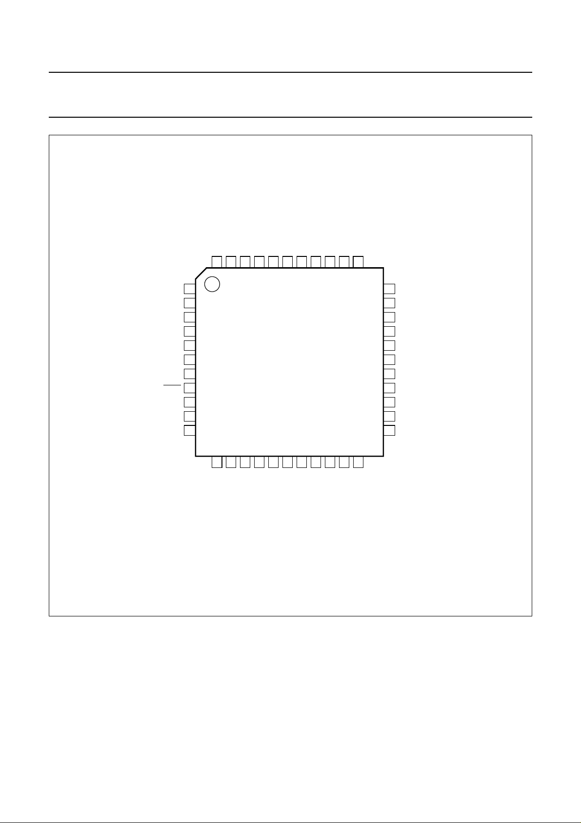
PACKAGE
SAF7113H QFP44 plastic quad flat package; 44 leads (lead length 1.3 mm); body 10 × 10 × 1.75 mm SOT307-2
2000 May 08 4

Philips Semiconductors Product specification
9-bit video input processor SAF7113H
6 BLOCK DIAGRAM
handbook, full pagewidth
MULTI-STANDARD DATA SLICER
AI11
AI1D
AI12
AOUT
AI21
AI2D
AI22
AGND
V
SSA1
V
SSA2
V
DDA1
V
DDA2
TCK
TMS
TRST
TDO
TDI
4
5
PROCESSING
7
9
ANALOG-TO-
43
CONVERSION
44
1
AD2 AD1
6
PROCESSING
2
41
3
42
38
37
CONTROL BLOCK
39
8
36
BOUNDARY
SCAN TEST
SCAN TEST
ANALOG
AND
DIGITAL
ANALOG
CONTROL
TEST
FOR
AND
CON
VBI DATA BYPASS
UPSAMPLING FILTER
bypass
CHROMINANCE
C/CVBS
Y/CVBS
CIRCUIT
AND
BRIGHTNESS CONTRAST
SATURATION CONTROL
LUMINANCE
CIRCUIT
Y
SYNCHRONIZATION
CIRCUIT
UV
Y
LFCO
Y
OUTPUT
FORMATTER
SAF7113H
2
I
C-BUS CONTROL
I2C-BUS
INTERFACE
CLOCKS
CLOCK
GENERATION
CIRCUIT
POWER-ON
CONTROL
12 to 15,
19 to 22
23
24
31
32
17
VPO7
to
VPO0
SDA
SCL
XTAL
XTALI
LLC
34 35
33 30
29 28
18 16
V
SSDI
V
SSDA
V
SSDE2
V
DDDE1
V
DDDI
V
DDDA
V
DDDE2
V
SSDE1
Fig.1 Block diagram.
2000 May 08 5
RTS0
26
RTS1
27
RTCO
40
11
V
DDA0
10
V
CE
SSA0
MHB690
25
Philips Semiconductors Product specification
9-bit video input processor SAF7113H
7 PINNING
SYMBOL PIN I/O/P DESCRIPTION
AI22 1 I analog input 22
V
SSA1
V
DDA1
AI11 4 I analog input 11
AI1D 5 I differential analog input for AI11 and AI12; has to be connected to ground via a
AGND 6 P analog signal ground connection
AI12 7 I analog input 12
TRST 8 I test reset input (active LOW), for boundary scan test; notes 1, 2 and 3
AOUT 9 O analog test output; for testing the analog input channels, 75 Ω termination possible
V
DDA0
V
SSA0
VPO7 to
VPO4
V
SSDE1
LLC 17 O line-locked system clock output (27 MHz)
V
DDDE1
VPO3 to
VPO0
SDA 23 I/O serial data input/output (I
SCL 24 I serial clock input (I
RTCO 25 (I/)O real-time control output: contains information about actual system clock frequency,
RTS0 26 (I/)O real-time signal output0: multi functional output, controlled by I
RTS1 27 I/O real-time signal I/O terminal 1: multi functional output, controlled by I
V
SSDI
V
DDDI
V
SSDA
XTAL 31 O second terminal of crystal oscillator; not connected if external clock signal is used
2 P ground for analog supply voltage channel 1
3 P positive supply voltage for analog channel 1 (+3.3 V)
capacitor; see application diagram of Fig.31
10 P positive supply voltage (+3.3 V) for internal Clock Generation Circuit (CGC)
11 P ground for internal clock generation circuit
12 to 15 O digital VPO-bus output signal; higher bits of the 8-bit output bus. The output data
2
types of the VPO-bus are controlled via I
C-bus registers LCR2 to LCR24;
see Table 4. If I2C-bus bit VIPB = 1, the higher bits of the digitized input signal are
connected to these outputs, configured by the I2C-bus control signals
MODE3 to MODE0
16 P ground 1 or digital supply voltage input E (external pad supply)
18 P digital supply voltage E1 (external pad supply 1; +3.3 V)
19 to 22 O digital VPO-bus output signal; lower bits of the 8-bit output bus. The output data types
2
of the VPO-bus are controlled via I
C-bus registers LCR2 to LCR24; see Table 4.
If I2C-bus bit VIPB = 1, the lower bits of the digitized input signal are connected to
these outputs, configured by the I2C-bus control signals MODE3 to MODE0
2
C-bus) 5 V-compatible
2
C-bus) 5 V-compatible
field rate, odd/even sequence, decoder status, subcarrier frequency and phase and
PAL sequence (see external document
“RTC Functional Description”
, available on
request); the RTCO pin is enabled via I2C-bus bit OERT; this pin is also used as an
input pin for test purposes and has an internal pull-down resistor; do not
connect any pull-up resistor to this pin
2
C-bus bits
RTSE03 to RTSE00; see Table 49. RTS0 is strapped during power-on or CE driven
reset, defines which I2C-bus slave address is used; 0 = 48H for write, 49H for read,
external pull-down resistor of 3.3 kΩ is needed; 1 = 4AH for write, 4BH for read,
default slave address (default, internal pull-up)
2
C-bus bit
RTSE13 to RTSE10; see Table 50
28 P ground for internal digital core supply
29 P internal core supply (+3.3 V)
30 P digital ground for internal crystal oscillator
2000 May 08 6

Philips Semiconductors Product specification
9-bit video input processor SAF7113H
SYMBOL PIN I/O/P DESCRIPTION
XTALI 32 I input terminal for crystal oscillator or connection of external oscillator with CMOS
compatible square wave clock signal
V
DDDA
V
DDDE2
V
SSDE2
TDO 36 O test data output for boundary scan test; note 3
TCK 37 I test clock for boundary scan test; note 3
TDI 38 I test data input for boundary scan test; note 3
TMS 39 I test mode select input for boundary scan test or scan test; note 3
CE 40 I chip enable, ‘sleep mode’ with low power consumption if connected to ground
V
SSA2
V
DDA2
AI21 43 I analog input 21
AI2D 44 I differential analog input for AI21 and AI22; has to be connected to ground via a
33 P digital positive supply voltage for internal crystal oscillator (+3.3 V)
34 P digital supply voltage E2 (external pad supply 2; +3.3 V)
35 P ground 2 for digital supply voltage input E (external pad supply)
(internal pull-up); internal reset sequence is generated when released
41 P ground for analog supply voltage channel 2
42 P positive supply voltage for analog channel 2 (+3.3 V)
capacitor; see application diagram of Fig.31
Notes
1. For board design without boundary scan implementation connect the TRST pin to ground.
2. This pin provides easy initialization of BST circuit. TRST can be used to force the Test Access Port (TAP) controller
to the TEST_LOGIC_RESET state (normal operation) at once.
3. In accordance with the
IEEE1149.1
standard the pads TCK, TDI, TMS and TRST are input pads with an internal
pull-up transistor and TDO is a 3-state output pad.
2000 May 08 7
Philips Semiconductors Product specification
9-bit video input processor SAF7113H
handbook, full pagewidth
DDDE2
AI2D
44
AI21
43
DDA2VSSA2
V
42
41
40
CE
TMS
39
TDI
TCK
383736
TDO
SSDE2
V
35
V
34
V
SSA1
V
DDA1
AI1D
AGND
TRST
AOUT
V
DDA0
V
SSA0
AI22
AI11
AI12
V
22
VPO0
33
32
31
30
29
28
27
26
25
24
23
MHB691
DDDA
XTALI
XTAL
V
SSDA
V
DDDI
V
SSDI
RTS1
RTS0
RTCO
SCL
SDA
1
2
3
4
5
6
7
8
9
10
11
12
13
VPO7
VPO6
14
VPO5
SAF7113H
15
16
VPO4
SSDE1
V
17
LLC
18
19
DDDE1
V
VPO3
20
VPO2
21
VPO1
Fig.2 Pin configuration.
2000 May 08 8

Philips Semiconductors Product specification
9-bit video input processor SAF7113H
8 FUNCTIONAL DESCRIPTION
8.1 Analog input processing
The SAF7113H offers four analog signal inputs, two
analog main channels with source switch, clamp circuit,
analog amplifier, anti-alias filter and video 9-bit CMOS
ADC; see Fig.6.
6
V
(dB)
0
−6
−12
−18
−24
−30
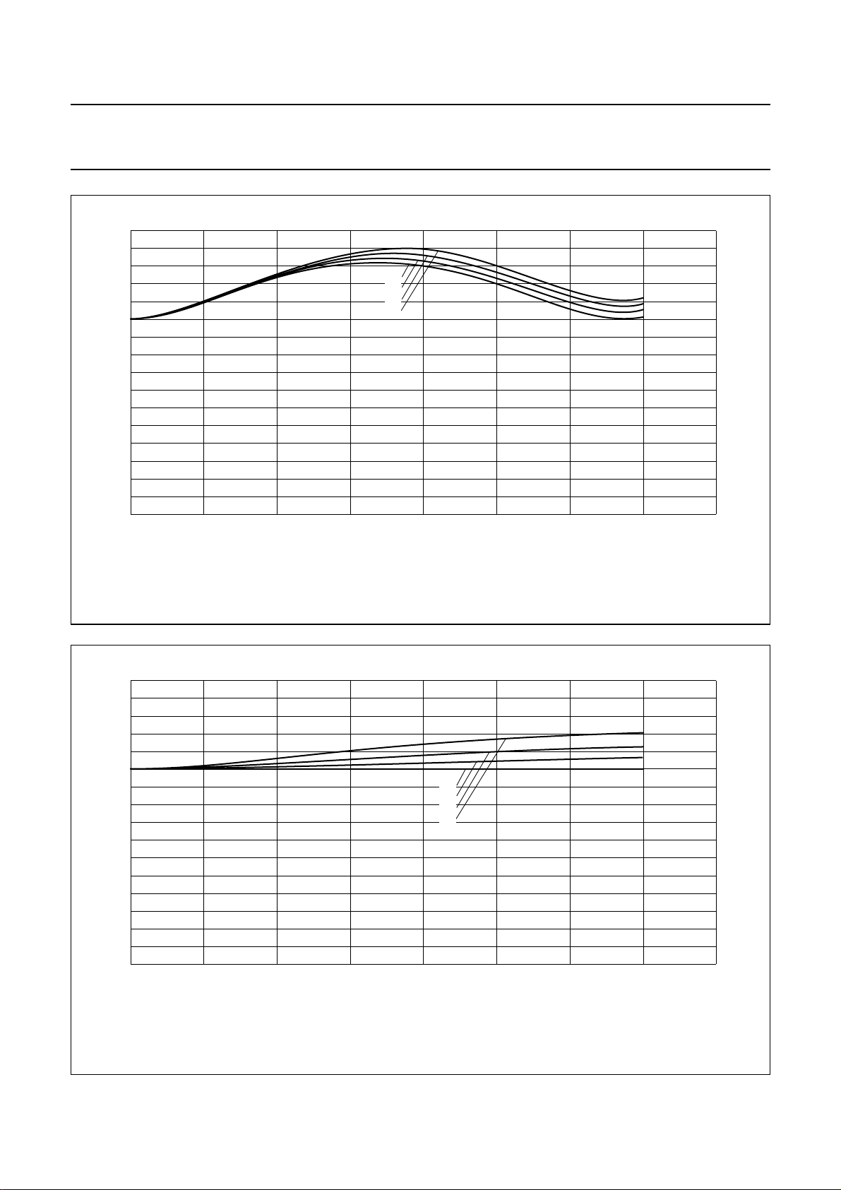
8.2 Analog control circuits
The anti-alias filters are adapted to the line-locked clock
frequency via a filter control circuit. The characteristics are
shown in Fig.3. During the vertical blanking period, gain
and clamping control are frozen.
MGD138
−36
−42
024 68101214
Fig.3 Anti-alias filter.
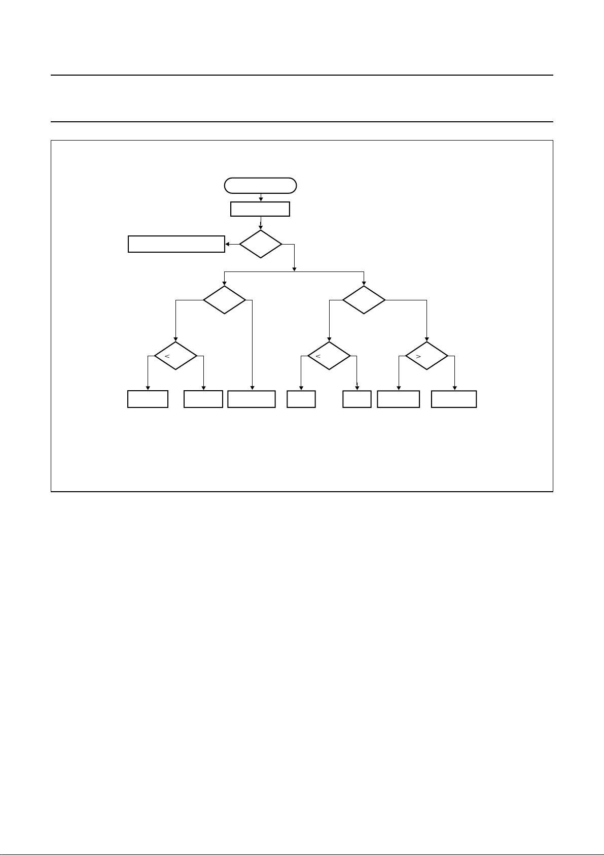
8.2.1 CLAMPING
The clamp control circuit controls the correct clamping of
the analog input signals. The coupling capacitor is also
used to store and filter the clamping voltage. An internal
digital clamp comparator generates the information with
respect to clamp-up or clamp-down. The clamping levels
for the two ADC channels are fixed for luminance (120)
and chrominance (256). Clamping time in normal use is
set with the HCL pulse at the back porch of the video
signal.
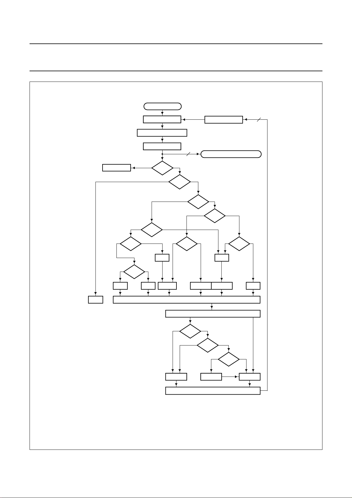
8.2.2 GAIN CONTROL
The gain control circuit receives (via the I2C-bus) the static
gain levels for the two analog amplifiers or controls one of
theseamplifiersautomaticallyviaabuilt-inAutomaticGain
Control (AGC) as part of the Analog Input Control (AICO).
The AGC (automatic gain control for luminance) is used to
amplify a CVBS or Y signal to the required signal
f (MHz)
amplitude, matched to the ADCs input voltage range.
The AGCactive time is the sync bottom ofthe video signal.
Signal (white) peak control limits the gain at signal
overshoots.Theflow charts (see Figs 7 and 8) show more
details of the AGC. The influence of supply voltage
variation within the specified range is automatically
eliminated by clamp and automatic gain control.
2000 May 08 9
Philips Semiconductors Product specification
9-bit video input processor SAF7113H
HSY
TV line
HCL
MGL065
analog line blanking
255
GAIN CLAMP
60
1
Fig.4 Analog line with clamp (HCL) and gain
range (HSY).
analog input level
+3 dB
0 dB
(1 V (p-p) 18/56 Ω)
−6 dB
Fig.5 Automatic gain range.
maximum
range 9 dB
minimum
controlled
ADC input level
0 dB
MHB325
2000 May 08 10

This text is here in white to force landscape pages to be rotated correctly when browsing through the pdf in the Acrobat reader.This text is here in
n
_white to force landscape pages to be rotated correctly when browsing through the pdf in the Acrobat reader.This text is here inThis text is here in
white to force landscape pages to be rotated correctly when browsing through the pdf in the Acrobat reader. white to force landscape pages to be ...
2000 May 08 11
dbook, full pagewidth
Philips Semiconductors Product specification
9-bit video input processor SAF7113H
V
SSA1
V
SSA2
V
DDA1
V
DDA2
AI22
AI2D
AI21
AI12
AI1D
AI11
2
41
1
44
43
3
42
7
5
4
SOURCE
SWITCH
SOURCE
SWITCH
MODE
CONTROL
MODE3
MODE2
MODE1
MODE0
CLAMP
CIRCUIT
CLAMP
CIRCUIT
CLAMP
CONTROL
HCL
GLIMB
GLIMT
WIPA
SLTCA
ANALOG
AMPLIFIER
DAC9
ANALOG
AMPLIFIER
DAC9
GAIN
CONTROL
HSY
HOLDG
GAFIX
WPOFF
GUDL[1:0]
GAI[28:20]
GAI[18:10]
HLNRS
UPTCV
ANTI-ALIAS
FILTER
ANTI-ALIAS
FILTER
ANTI-ALIAS
CONTROL
BYPASS
SWITCH
FUSE[1:0]
BYPASS
SWITCH
FUSE[1:0]
VERTICAL
BLANKING
CONTROL
VBLNK
VBSL
SVREF
ANALOG CONTROL
TEST
SELECTOR
AND
BUFFER
AOSL[1:0]
ADC2
ADC1
99
9
AOUT
AGND
6
CHRLUM
CROSS MULTIPLEXER
MHB326
AD1BYPAD2BYP
Fig.6 Analog input processing using the SAF7113H as differential front-end with 9-bit ADC.
Philips Semiconductors Product specification
9-bit video input processor SAF7113H
handbook, full pagewidth
NO ACTION
0
1
ANTI-ALIAS FILTER
0
1
<4
0
>248
ANALOG INPUT
AMPLIFIER
ADC
1
VBLK
1
HOLDG
1
>254
1
X = 0
gain
9
0
0
1
X
1
0
<1
DAC
LUMA/CHROMA DECODER
0
0
HSY
1
>254
X = 1
9
0
+1/F
STOP
X = system variable; Y = (IAGV − FGVI) > GUDL; VBLK = vertical blanking pulse;
HSY = horizontal sync pulse; AGV = actual gain value; FGV = frozen gain value.
+1/L
−1/LLC2
GAIN ACCUMULATOR (18 BITS)
ACTUAL GAIN VALUE 9-BIT (AGV) [−6/+6 dB]
1
AGV
Fig.7 Gain flow chart.
+1/LLC2 −1/LLC2
0
X
1
HSY
1
UPDATE
GAIN VALUE 9-BIT
+/− 0
0
0
Y
FGV
MHB327
2000 May 08 12
Philips Semiconductors Product specification
9-bit video input processor SAF7113H
ANALOG INPUT
ADC
NO BLANKING ACTIVE
10 10
10
CLL
+ CLAMP − CLAMP
WIPE = white peaklevel (254); SBOT = sync bottomlevel (1); CLL = clamp level[60 Y (128 C)];
HSY = horizontal sync pulse; HCL = horizontal clamp pulse.
10
VBLK
HCL HSY
01 10
SBOT
NO CLAMP
+ GAIN − GAIN
Fig.8 Clamp and gain flow.
8.3 Chrominance processing
The 9-bit chrominance signal is fed to the multiplication
inputs of a quadrature demodulator, where two subcarrier
signals from the local oscillator DTO1 are applied
(0 and 90° phase relationship to the demodulator axis).
The frequency is dependent on the present colour
standard. The output signals of the multipliers are
low-pass filtered (four programmable characteristics) to
achieve the desired bandwidth for the colour difference
signals (PAL, NTSC) or the 0 and 90° FM signals
(SECAM).
The colour difference signals are fed to the
Brightness/Contrast/Saturation block (BCS), which
includes the following five functions:
• AGC (automatic gain control for chrominance
PAL and NTSC)
• Chrominance amplitude matching (different gain factors
for (R − Y) and (B − Y) to achieve ITU-R BT.601 levels
CRand CB for all standards)
• Luminance contrast and brightness
• Limiting YUV to the values 1 (minimum) and 254
(maximum) to fulfil ITU-R BT.601 requirements.
The SECAM-processing contains the following blocks:
• Baseband ‘bell’ filters to reconstruct the amplitude and
phase equalized 0 and 90° FM signals
• Phase demodulator and differentiator
(FM-demodulation)
• De-emphasis filter to compensate the pre-emphasized
input signal, including frequency offset compensation
(DB or DR white carrier values are subtracted from the
signal, controlled by the SECAM switch signal).
The burst processing block provides the feedback loop of
the chrominance PLL and contains:
• Burst gate accumulator
• Colour identification and killer
• Comparisonnominal/actualburst amplitude (PAL/NTSC
standards only)
• Chrominance saturation control
GAIN -><- CLAMP
WIPE
fast − GAIN
slow + GAIN
MGC647
2000 May 08 13

Philips Semiconductors Product specification
9-bit video input processor SAF7113H
• Loop filter chrominance gain control (PAL/NTSC
standards only)
• Loop filter chrominance PLL (only active for PAL/NTSC
standards)
• PAL/SECAM sequence detection, H/2-switch
generation
• Increment generation for DTO1 with divider to generate
stable subcarrier for non-standard signals.
The chrominance comb filter block eliminates crosstalk
betweenthechrominancechannels in accordance withthe
PAL standard requirements.
V
(dB)
−12
−18
6
0
−6
(1)
(2)
(3)
(4)
handbook, full pagewidth
For NTSC colour standards the chrominance comb filter
can be used to eliminate crosstalk from luminance to
chrominance (cross-colour) for vertical structures.
The comb filter can be switched off if desired.
The embedded line delay is also used for SECAM
recombination (cross-over switches).
The resulting signals are fed to the variable Y-delay
compensationand the output interface, which contains the
VPO output formatter and the output control logic,
see Fig.10.
MGD147
−24
−30
−36
−42
−48
−54
0 0.54 1.08 1.62 2,16
Transfer characteristics of the chrominance low-pass dependent on CHBW[1:0] settings.
(1) CHBW[1:0] = 00.
(2) CHBW[1:0] = 01.
(3) CHBW[1:0] = 10.
(4) CHBW[1:0] = 11.
Fig.9 Chrominance filter.
(4)
(1)
(3)
(2)
f
(MHz)
2.7
2000 May 08 14

This text is here in white to force landscape pages to be rotated correctly when browsing through the pdf in the Acrobat reader.This text is here in
n
_white to force landscape pages to be rotated correctly when browsing through the pdf in the Acrobat reader.This text is here inThis text is here in
white to force landscape pages to be rotated correctly when browsing through the pdf in the Acrobat reader. white to force landscape pages to be ...
2000 May 08 15
dbook, full pagewidth
Philips Semiconductors Product specification
9-bit video input processor SAF7113H
V
DDDE1
V
V
DDDA
V
DDDE2
V
SSDE1
V
V
SSDA
V
SSDE2
TRST
TCK
TDI
TMS
TDO
DDDI
SSDI
8
37
38
39
36
18
29
33
34
16
28
30
35
TEST
CONTROL
BLOCK
RESET
POWER-ON
CONTROL
CE
CLOCKS
CHRLUM
QUADRATURE
DEMODULATOR
SUBCARRIER
GENERATION
HUEC
VBI DATA BYPASS
UPSAMPLING
FILTER
DATA SLICER
INPUT
CHBW0
CHBW1
SUBCARRIER
INCREMENT
GENERATION
AND
DIVIDER
INCS
LOW-PASS
PHASE
DEMODULATOR
AMPLITUDE
DETECTOR
BURST GATE
ACCUMULATOR
LOOP FILTER
CODE
FCTCCSTD[2:0]
MULTI-STANDARD DATA SLICER
COMPENSATION
BRIG
CONT
SATN
SECAM
PROCESSING
sequential
UV signals
LEVEL
ADJUSTMENT,
BRIGHTNESS,
CONTRAST,
AND
SATURATION
CONTROL
GAIN
CONTROL
AND Y-DELAY
Y
UV
fH/2 switch signal
MULTI-STANDARD DATA SLICER
COMB
FILTERS
SECAM
RECOMBINATION
DCCF
INTERFACING
UV
AD1BYPAD2BYP
OUTPUT
FORMATTER
AND
INTERFACE
OFTS0
OFTS1
OEYC
OEHV
VRLN
VSTA[8:0]
VSTO[8:0]
12, 13, 14,
15, 19, 20,
GPSW[1:0]
RTSE1[3:0]
RTSE0[3:0]
VIPB
COLO
21, 22
VPO7
to
VPO0
25
RTCO
LUM
Y
Fig.10 Chrominance circuit, text slicer, VBI-bypass, output formatting, power and test control.
MHB328

Philips Semiconductors Product specification
9-bit video input processor SAF7113H
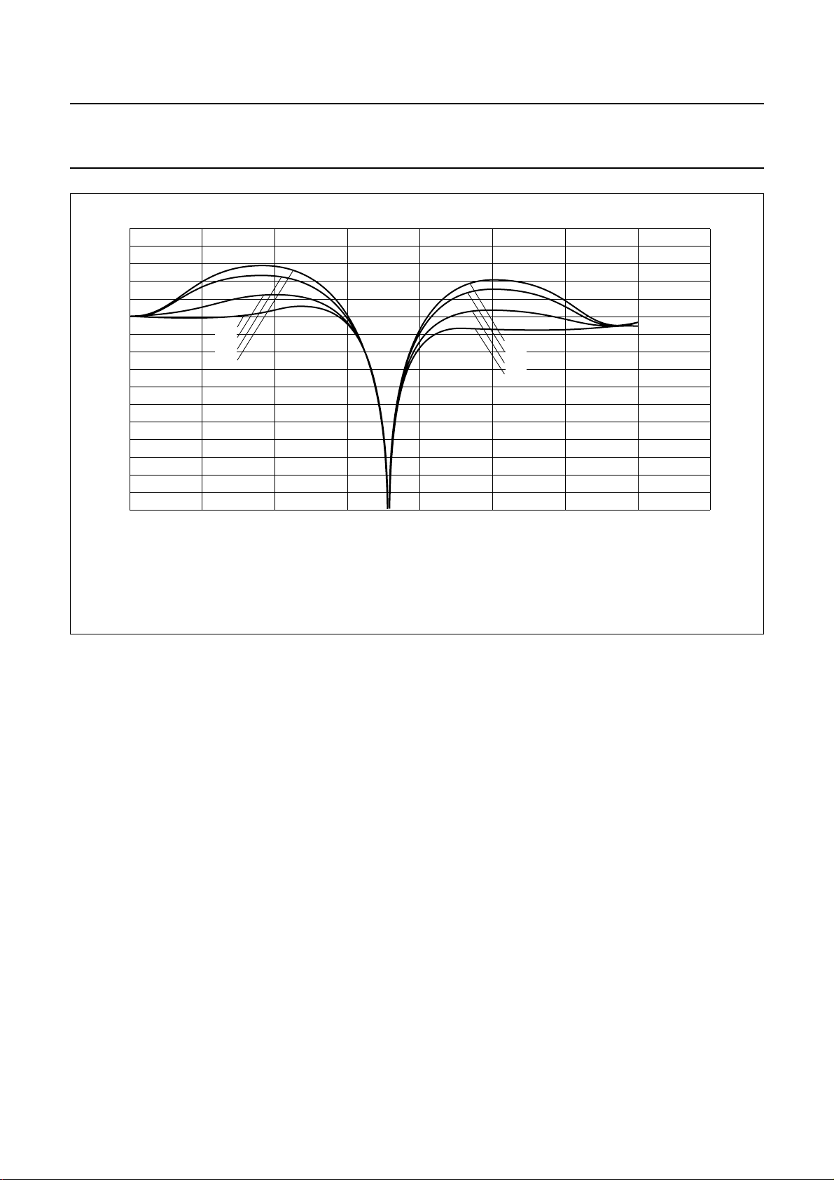
8.4 Luminance processing
The 9-bit luminance signal, a digital CVBS format or a
luminance format (S-VHS, HI8), is fed through a
switchable prefilter. High frequency components are
emphasized to compensate for loss. The following
chrominance trap filter (f0= 4.43 or 3.58 MHz centre
frequency set according to the selected colour standard)
eliminates most of the colour carrier signal. It should be
bypassed via I2C-bit BYPS (subaddress 09H, bit 7) for
S-video (S-VHS, HI8) signals.
18
handbook, full pagewidth
V
Y
(dB)
6
−6
(1)
(2)
(4)
(3)
The high frequency components of the luminance signal
can be peaked (control for sharpness improvement via
I2C-bus subaddress 09H, see Table 36) in two band-pass
filters with selectable transfer characteristic. This signal is
then added to the original (unpeaked) signal. For the
resulting frequency characteristics see Figs 11 to 18.
A switchableamplifierachieves commonDCamplification,
because the DC gains are different in both chrominance
trap modes. The improved luminance signal is fed to the
BCS control located in the chrominance processing block,
see Fig.19.
MGD139
(1)
(2)
(4)
(3)
−18
−30
024 86
(1) 43H. (2) 53H. (3) 63H. (4) 73H.
f
Y (MHz)
Fig.11 Luminance control SA 09H, 4.43 MHz trap/CVBS mode, prefilter on, different aperture band-pass centre
frequencies.
2000 May 08 16

Philips Semiconductors Product specification
9-bit video input processor SAF7113H
18
handbook, full pagewidth
V
Y
(dB)
6
(1)
(2)
(3)
(4)
−6
−18
−30
024 86
(1) 40H. (2) 41H. (3) 42H. (4) 43H.
Fig.12 Luminance control SA 09H, 4.43 MHz trap/CVBS mode, prefilter on, different aperture factors.
(4)
(3)
(2)
(1)
f
Y (MHz)
MGD140
18
handbook, full pagewidth
V
Y
(dB)
6
−6
−18
−30
024 86
(1) 03H.
(1)
(2)
(4)
(3)
(2) 13H. (3) 23H. (4) 33H.
(1)
(2)
(4)
(3)
f
Y (MHz)
MGD141
Fig.13 Luminance control SA 09H, 4.43 MHz trap/CVBS mode, prefilter off, different aperture band-pass centre
frequencies.
2000 May 08 17
Philips Semiconductors Product specification
9-bit video input processor SAF7113H
18
handbook, full pagewidth
V
Y
(dB)
6
−6
−18
−30
024 86
(1) C0H. (2) C1H. (3) C2H. (4) C3H.
(1)
(2)
(3)
(4)
Fig.14 Luminance control SA 09H, Y/C mode, prefilter on, different aperture factors.
f
Y (MHz)
MGD142
18
handbook, full pagewidth
V
Y
(dB)
6
(1)
(2)
(3)
−6
−18
−30
024 86
(1) 80H. (2) 81H. (3) 82H. (4) 83H.
(4)
Fig.15 Luminance control SA 09H, Y/C mode, prefilter off, different aperture factors.
f
Y (MHz)
MGD143
2000 May 08 18

Philips Semiconductors Product specification
9-bit video input processor SAF7113H
18
handbook, full pagewidth
V
Y
(dB)
6
−6
−18
−30
024 86
(1) 43H. (2) 53H. (3) 63H. (4) 73H.
(1)
(2)
(4)
(3)
(1)
(2)
(4)
(3)
f
Y (MHz)
MGD144
Fig.16 Luminance control SA 09H, 3.58 MHz trap/CVBS mode, prefilter on, different aperture band-pass centre
frequencies.
18
handbook, full pagewidth
V
Y
(dB)
6
−6
−18
−30
024 86
(1) 40H. (2) 41H. (3) 42H. (4) 43H.
(1)
(2)
(3)
(4)
Fig.17 Luminance control SA 09H, 3.58 MHz trap/CVBS mode, prefilter on, different aperture factors.
(4)
(3)
(2)
(1)
f
Y (MHz)
MGD145
2000 May 08 19
Philips Semiconductors Product specification
9-bit video input processor SAF7113H
18
handbook, full pagewidth
V
Y
(dB)
6
(1)
(2)
(4)
−6
−18
−30
024 86
(1) 03H. (2) 13H. (3) 23H. (4) 33H.
(3)
(1)
(2)
(4)
(3)
f
Y (MHz)
MGD146
Fig.18 Luminance control SA 09H, 3.58 MHz trap/CVBS mode, prefilter off, different aperture band-pass centre
frequencies.
2000 May 08 20

This text is here in white to force landscape pages to be rotated correctly when browsing through the pdf in the Acrobat reader.This text is here in
n
_white to force landscape pages to be rotated correctly when browsing through the pdf in the Acrobat reader.This text is here inThis text is here in
white to force landscape pages to be rotated correctly when browsing through the pdf in the Acrobat reader. white to force landscape pages to be ...
2000 May 08 21
LUM
PREFILTER
LUMINANCE CIRCUIT
CHROMINANCE
TRAP
VARIABLE
BAND-PASS
FILTER
dbook, full pagewidth
Y
WEIGHTING
AND
ADDING
STAGE
Philips Semiconductors Product specification
9-bit video input processor SAF7113H
PREF
PREFILTER
SYNC
BYPS
VBLB
MACROVISION
DETECTOR
SYNC SLICER
SYNCHRONIZATION CIRCUIT
2
I
C-BUS CONTROL
2
C-BUS
I
INTERFACE
24 23 26 27
SDASCL
VNOI0
VNOI1
HTC[1:0]
VERTICAL
PROCESSOR
RTS0
BPSS0
BPSS1
PREF
COPRO
PHASE
DETECTOR
AUFD
HSB[7:0]
HSS[7:0]
FSELFIDT
COUNTER
RTS1
FINE
HLCK
MATCHING
AMPLIFIER
VBLB
DETECTOR
HPLL
HTC[1:0]
LOOP FILTER
PHASE
COARSE
HTC[1:0]
2
APER0
APER1
VBLB
INCS
DISCRETE
OSCILLATOR 2
CLOCK CIRCUIT
DAC6
TIME
CLOCKS
LINE-LOCKED
CLOCK
GENERATOR
CLOCK
GENERATION
CIRCUIT
CRYSTAL
CLOCK
GENERATOR
17
10
11
40
32
31
MHB329
LLC
V
DDA0
V
SSA0
CE
XTALI
XTAL
Fig.19 Luminance and sync processing.

Philips Semiconductors Product specification
9-bit video input processor SAF7113H
8.5 Synchronization
The prefiltered luminance signal is fed to the
synchronization stage. Its bandwidth is further reduced to
1 MHz in a low-pass filter. The sync pulses are sliced and
fed to the phase detectors where they are compared with
the sub-divided clock frequency. The resulting output
signal is applied to the loop filter to accumulate all phase
deviations. Internal signals (e.g. HCL and HSY) are
generated in accordance with analog front-end
requirements. The loop filter signal drives an oscillator to
generate the line frequency control signal LFCO,
see Fig.19.
The detection of ‘pseudo syncs’ as part of the macrovision
copy protection standard is also done within the
synchronization circuit.
The result is reported as flag COPRO within the decoder
status byte at subaddress 1FH.
LFCO
BAND PASS
FC = LLC/4
ZERO
CROSS
DETECTION
DETECTION
8.6 Clock generation circuit
The internal CGC generates all clock signals required for
the video input processor. The internal signal LFCO is a
digital-to-analog converted signal provided by the
horizontal PLL. It is the multiple of the line frequency
[6.75 MHz = 429 × fH (50 Hz) or 432 × fH (60 Hz)].
Internally the LFCO signal is multiplied by a factor of
2 and 4 in the PLL circuit (including phase detector, loop
filtering, VCO and frequency divider) to obtain the output
clock signals. The rectangular output clocks have a 50%
duty factor.
PHASE
LOOP
FILTER
OSCILLATOR
LLC
Table 1 Clock frequencies
CLOCK FREQUENCY (MHz)
XTAL 24.576
LLC 27
LLC2 (internal) 13.5
LLC4 (internal) 6.75
LLC8 (virtual) 3.375
DIVIDER
1/2
Fig.20 Block diagram of clock generation circuit.
8.7 Power-on reset and CE input
A missing clock, insufficient digital or analog V
voltages (below 2.8 V) will initiate the reset sequence; all
outputs are forced to 3-state (see Fig.21).
It is possible to force a reset by pulling the Chip Enable
(CE) to ground. After the rising edge of CE and sufficient
power supply voltage, the outputs LLC and SDA return
from 3-state to active, while RTS0, RTS1 and RTCO
remain in 3-state and have to be activated via I2C-bus
programming (see Table 2).
DIVIDER
1/2
MHB330
LLC2
DDA0
supply
2000 May 08 22

Philips Semiconductors Product specification
9-bit video input processor SAF7113H
CE
XTALO
LLCINT
RESINT
CE
CLOCK
PLL
LLC
POC V
ANALOG
POC
LOGIC
DDA
RESINT
POC V
DIGITAL
POC
DELAY
CLK0
DDD
RES
LLC
RES
(internal
reset)
CE = chip enable input; XTAL = crystal oscillator output; LLCINT = internal system clock;
RESINT = internal reset; LLC = line-locked clock output.
some ms
20 to 200 µs
PLL-delay
<
1 ms
Fig.21 Power-on control circuit.
2000 May 08 23
896 LCC
digital delay
128 LCC
MHB331

Philips Semiconductors Product specification
9-bit video input processor SAF7113H
Table 2 Power-on control sequence
INTERNAL POWER-ON
CONTROL SEQUENCE
Directly after power-on
asynchronous reset
Synchronous reset
sequence
Status after power-on
control sequence
8.8 Multi-standard VBI data slicer
The multi-standard data slicer is a Vertical Blanking
Interval (VBI) and Full Field (FF) video data acquisition
block. In combination with software modules the slicer
acquires most existing formats of broadcast VBI and FF
data.
The implementation and programming model of the
multi-standard VBI data slicer is similar to the text slicer
built in the
SAA5284”
The circuitry recovers the actual clock phase during the
clock-run-in-period, slices the data bits with the selected
data rate, and groups them into bytes. The clock
frequency, signals source, field frequency and accepted
error count must be defined via the I2C-bus in
subaddress 40H, AC1: bits D7 to D4.
“Multimedia Video Data Acquisition Circuit
.
VPO7 to VPO0, RTCO, RTS0, RTS1,
SDA and LLC are in high-impedance state
LLC and SDA become active;
VPO7 to VPO0, RTCO,RTS0 and RTS1 are
held in high-impedance state
VPO7 to VPO0, RTCO,RTS0 and RTS1 are
held in high-impedance state
PIN OUTPUT STATUS REMARKS
direct switching to high-impedance for
20 to 200 ms
internal reset sequence
after power-on (reset sequence) a complete
2
C-bus transmission is required
I
Several standards can be selected per VBI line.
The supported VBI data standards are described in
Table 3.
The programming of the desired standards is done via
I2C-bus subaddresses 41H to 57H
(LCR2[7 : 0] to LCR24[7 : 0]); see detailed description in
Chapter 8.10. To adjust the slicers processing to the
signals source, there are offsets in horizontal and vertical
direction available via the I2C-bus in subaddresses 5BH
(bits 2 to 0), 59H (HOFF10 to HOFF0) and 5BH (bit 4),
5AH (VOFF8 to VOFF0). The formatting of the decoded
VBI data is done within the output interface to the
VPO-bus. For a detailed description of the sliced data
format see Table 17.
Table 3 Supported VBI standards
STANDARD TYPE
Teletext EuroWST, CCST 6.9375 27H WST625 always
European closed caption 0.500 001 CC625
VPS 5 9951H VPS
Wide screen signalling bits 5 1E3C1FH WSS
US teletext (WST) 5.7272 27H WST525 always
US closed caption (line 21) 0.503 001 CC525
Teletext 6.9375 programmable general text optional
VITC/EBU time codes (Europe) 1.8125 programmable VITC625
VITC/SMPTE time codes (USA) 1.7898 programmable VITC625
US NABTS 5.7272 programmable NABTS optional
MOJI (Japanese) 5.7272 programmable (A7H) Japtext
Japanese format switch (L20/22) 5 programmable
2000 May 08 24
DATA RATE
(Mbits/s)
FRAMING CODE
FC
WINDOW
HAM
CHECK
 Loading...