

Philips saf1135 DATASHEETS

INTEGRATED CIRCUITS
DATA SH EET
SAF1135
Data line decoder
Product specification
File under Integrated Circuits, IC02
August 1986
Philips Semiconductors Product specification
Data line decoder SAF1135
GENERAL DESCRIPTION
The SAF1135 is a data line decoder, designed in CMOS technology, which operates in conjunction with the data line
processor (SAA5235) to form a data line receiver system.
This system receives and decodes binary data that is transmitted in line 16 of every first field of a standard television
signal. The decoded information is accessed via the built-in I2C bus interface. This information can be used to program
a video tape recorder to start and stop the recording of a television program at the correct time, regardless of a delay or
extension in the transmission time of the required television program.
Valid Video Programming System (VPS) data is transmitted in line 16 only. There is no VPS information in line 329.
The data transmission is biphase modulated and the bit transfer rate is 2,5 Mbit/s.
Features
• Field selection
• Line 16 decoding
• Start code check
• Biphase check
• Storage of data line information
• Generation of data reset pulse
2
C bus transmitter
• I
QUICK REFERENCE DATA
PARAMETER SYMBOL MIN. TYP. MAX. UNIT
Supply voltage (pin 14) V
Supply current (pin 14) I
DD
Bit transfer rate at input DLD (pin 8) BR
Clock frequency at input DLCL (pin 11) f
DLCL
Storage temperature range T
Operating ambient temperature range T
PACKAGE OUTLINES
14-lead DIL; plastic (SOT27); SOT27-1; 1997 January 07.
DD
stg
amb
DLD
4,5 5,0 5,5 V
− 1 − mA
− 2,5 − Mbits/s
− 5 − MHz
−65 −+150 °C
0 − 70 °C
August 1986 2
Philips Semiconductors Product specification
Data line decoder SAF1135
August 1986 3
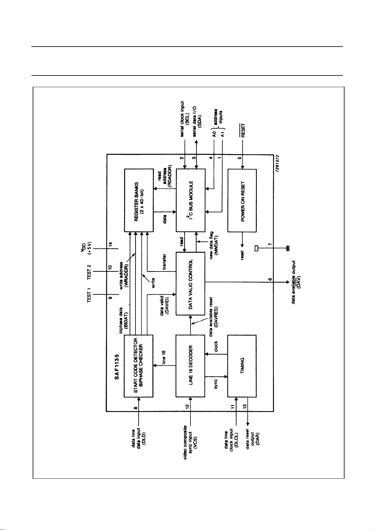
Fig.1 Block diagram.

Philips Semiconductors Product specification
Data line decoder SAF1135
FUNCTIONAL DESCRIPTION
The SAF1135 is designed to receive and decode Video Tape Recorder (VTR) control information which is transmitted in
line 16 of every first field of a standard television signal. The following description refers to the block diagram Fig.1 unless
otherwise stated.
Data line 16
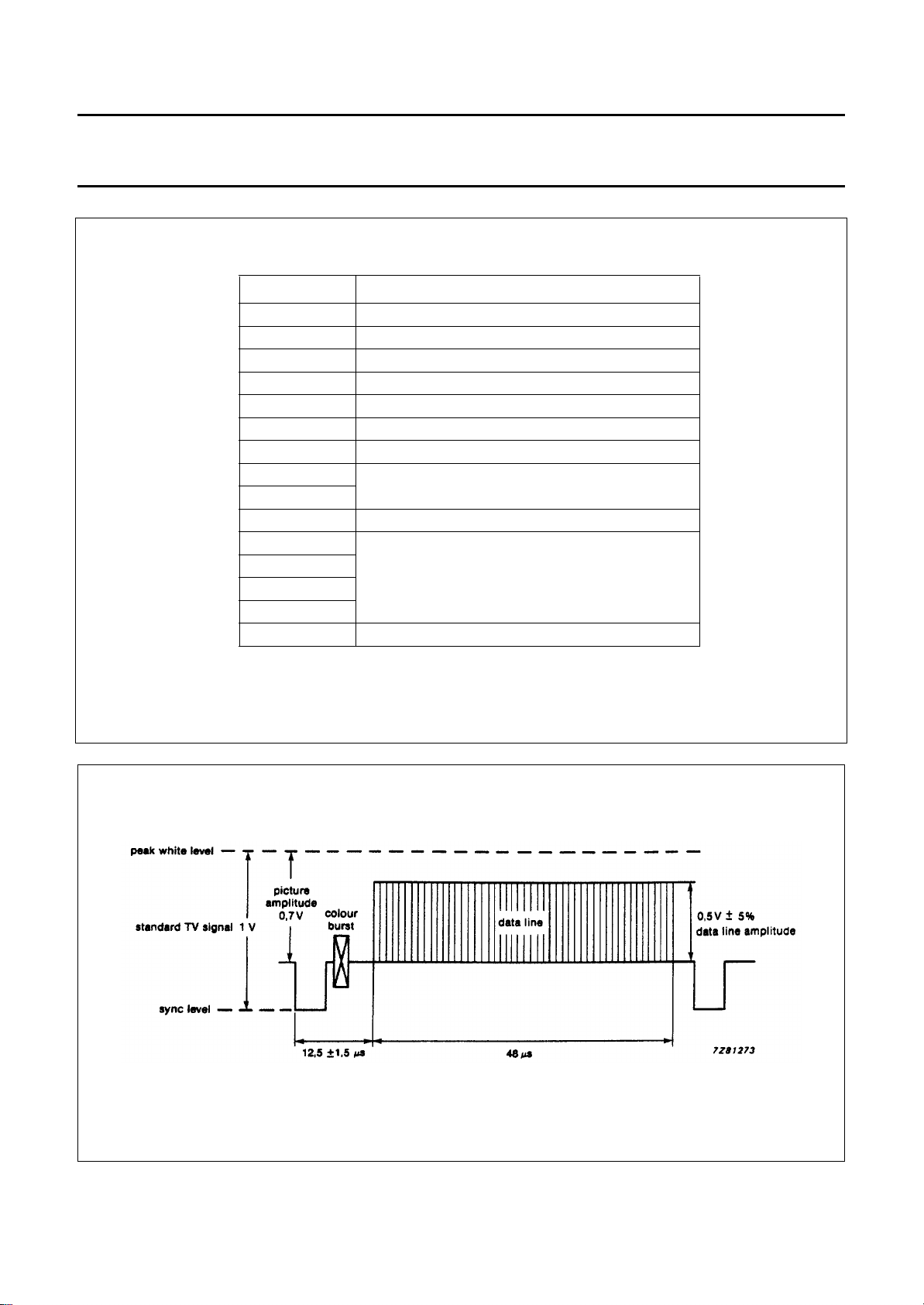
The total information of data line 16 consists of fifteen 8-bit words. The contents of the information is shown in Fig.2, a
timing diagram of the data line in Fig.3 and a survey of VTR control labels in Fig.4.
From the total fifteen 8-bit words, the SAF1135 extracts words 5, 11, 12, 13 and 14. The contents of these words can be
requested via the built-in I
modification. Only the sequence of the words is changed; words 11 to 14 being transmitted first followed by word 5.
By evaluation of the Video Composite Sync (VCS) signal at pin 12 the SAF1135 identifies the beginning of line 16 in the
first field. The line 16 decoder stage releases the start code detector. When a correct start code is detected (for timing
of start code detection, see Fig.5) words 5 and 11 to 14 are decoded, checked for biphase errors and stored in register
bank R (Receive). If no biphase error has occurred, the contents of register bank R are transferred to register bank T
(Transmit) by the data valid control signal (DAVID). If the system has been addressed, this transfer is delayed until the
next start or stop condition of the I2C bus has been received.
The last correct data line information remains available until it is read via the I2C bus. After it is read once the stored
information is no longer considered to be valid, the internal new data flag (NWDAT) is reset and if the circuit is addressed,
the only VPS data sent back is “FFF...F”. The same conditions apply after power-up. Then no data can be read out.
New data is available after reception of another error-free line 16.
Power-on Reset
Reset pulses applied externally to pin 5 (
RESET = LOW influences:
• I2C bus logic to no acknowledge
• NWDAT flag and internal timing to reset
• Data available output (DAV; active LOW) at pin 6 forced to LOW
• Data reset output (DAR) at pin 13 forced to HIGH
• Serial data (SDA) input/output at pin 3 released
2
C bus interface (see Fig.9). The circuit is fully transparent, thus each bit is transferred without
RESET; active LOW) are latched internally by the power-on reset circuit.
When RESET changes to HIGH the reset period is terminated with the next negative-going transition of the data line
clock (DLCL) input at pin 11. Then, the data available (DAV) output at pin 6 will go HIGH.
When an external reset is not used pin 5 is connected to VDD. If an external reset is required, the rise time (tr) of RESET
voltage must be greater than 50 µs. An external 10 kΩ resistor connected between pin 5 and VDD and an external 2,7 nF
capacitor connected to VSS will result in tr≥ 50 µs.
August 1986 4
Philips Semiconductors Product specification
Data line decoder SAF1135
WORD CONTENT
1 Run in
2 Start code
3 Program source identification (binary coded)
4 Program source identification (ASCII sequential)
5 Sound and VTR control information
6 Program/Test picture identification
7 Internal information exchange
8
9
10 Messages/Commands
11
12
13
14
15 Reserve
Address assignment of signal distribution
VTR Control Information
Fig.2 Total information of data line 16.
Fig.3 Timing diagram of data line 16; modulation depth 71,4%.
August 1986 5
 Loading...