

Philips SAB9082 Datasheet
INTEGRATED CIRCUITS
DATA SH EET
SAB9082
NTSC Picture-In-Picture (PIP)
controller
Preliminary specification
File under Integrated Circuits, IC02
1999 Feb 18
Philips Semiconductors Preliminary specification
NTSC Picture-In-Picture (PIP) controller SAB9082
FEATURES
• Double window PIP in interlaced mode at 8-bit
resolution
• Internal DRAM of 1 Mbit
• Three 8-bit Analog-to-Digital Converters (ADCs) (7-bit
performance) with clamp circuit for each acquisition
channel
• One PLL which generates the line-locked clocks for the
subchannel
• One PLL which generates the line-locked clocks for the
main and display channel
• Three 8-bit Digital-to-Analog Converters (DACs)
• Linear zoom in both horizontal and vertical direction for
the subchannel
• Linear zoom in horizontal direction for the main channel
• Three multi PIP modes are available.
GENERAL DESCRIPTION
The SAB9082 is an NTSC Picture-in-Picture controller
which can be used in double window applications.
It inserts one or two live video signals with reduced size
into another live video signal. The incoming video signals
are expected to be analog baseband signals.
The conversion into the digital environment is done on
chip with ADCs. Processing and storage of the video data
is done entirely in the digital domain. The conversion back
to the analog domain is done by means of DACs. Internal
clocks are generated by PLLs which lock on to the applied
horizontal and vertical syncs.
The main input channel is compressed horizontally with a
factor of 2 and directly fed to the output. After compressing
a horizontal expansion of 2 is possible for the main
channel.
The subchannel is also compressed horizontally with a
factor of 2 but stored in memory before it is fed to the
outputs.
The SAB9082 can also create three multi PIP modes, one
with three PIPs placed in a column (MP3) and two with two
columns of three PIPs (MP6, MP6S). The reduction factors
of these PIPs is horizontal 1/2 and vertical 1/3. In the first
two modes the column(s) can be placed on the left or right
side of the screen.
QUICK REFERENCE DATA
SYMBOL PARAMETER CONDITIONS MIN. TYP. MAX. UNIT
Supply
V
V
I
DDD
I
DDA
DDD
DDA
digital supply voltage 3.0 3.3 3.6 V
analog supply voltage 3.0 3.3 3.6 V
digital supply current tbf 65 tbf mA
analog supply current tbf 185 tbf mA
PLL
f
sys
B
t
jitter
loop
system frequency 1792×HSYNC − 28 − MHz
loop bandwidth − 4 − kHz
short term stability jitter during 64 µs −−4ns
ζ damping factor − 0.7 −
ORDERING INFORMATION
TYPE
NUMBER
NAME DESCRIPTION VERSION
SAB9082 QFP100 plastic quad flat package; 100 leads (lead length 1.95 mm);
PACKAGE
SOT317-2
body 14 × 20 × 2.8 mm
1999 Feb 18 2
This text is here in white to force landscape pages to be rotated correctly when browsing through the pdf in the Acrobat reader.This text is here in
_white to force landscape pages to be rotated correctly when browsing through the pdf in the Acrobat reader.This text is here inThis text is here in
white to force landscape pages to be rotated correctly when browsing through the pdf in the Acrobat reader. white to force landscape pages to be ...
1999 Feb 18 3
handbook, full pagewidth
BLOCK DIAGRAM
NTSC Picture-In-Picture (PIP) controller SAB9082
Philips Semiconductors Preliminary specification
V
bias(SA)
V
ref(T)(SA)
V
ref(B)(SA)
SHSYNC
SVSYNC
V
bias(MA)
V
ref(T)(MA)
V
ref(B)(MA)
SU
SV
SY
MU
MY
MV
V
DDA(MF)
79
81
83
84
82
80
87
72
2
98
100
97
99
1
V
SSA(MA)
V
DDA(MA)
34
V
DDA(DA)
56
CLAMP AND ADC
PLL AND CLOCK
GENERATOR
CLAMP AND ADC
V
SSA(DA)
V
714
DDD(DA)
V
SSD(DA)
V
SSD(P1)
15 16
V
DDD(RP)
V
DDD(P1)
17 20
HORIZONTAL
AND
VERTICAL
FILTER
LINE MEMORY INTERNAL DRAM
HORIZONTAL
FILTER
V
DDD(RL)
V
SSD(RL)
V
39 40
V
DDD(RM)
SSD(RM)
41 42
V
SSD(RP)
V
DDD(P2)
61 64
V
SSD(P2)
V
SSD(D)
V
DDD(D)
65 66
SAB9082
V
DDA(SA)
67 76
DAC AND BUFFER
V
V
SSA(SA)
77 78
DISPLAY
CONTROL
DDA(SF)
V
SSD(SA)
V
DDD(SA)
85 86
18, 19
48 to 51
62, 63
8
10
12
9
11
13
69
68
30
DY
DV
DU
V
bias(DA)
V
ref(T)(DA)
V
ref(B)(DA)
PKOFF
FBL
V
SSD(T1, T2)
V
SSD(T3)
V
SSD(T4 to T7)
V
SSD(T8, T9)
DHSYNC
DVSYNC
94
70
V
DDA(SP)
PLL AND CLOCK
GENERATOR
89
90 91 92 95
V
SSA(DP)
V
SSA(SP)
V
DDA(DP)
V
DDD(MA)
V
SSD(MA)
96
21 to 29, 31,
52 to 60
n.c.
2
I
C-BUS
CONTROL
74
75
SDA
POR
Fig.1 Block diagram.
TEST
CONTROL
73 88 93 44 43 45 46 47
T7
T6
SCL
TCBD TCBR
TCLKTMTCBC
32 to 37
MGL582
71
DCLK
38
TC
T5 to T0
Philips Semiconductors Preliminary specification
NTSC Picture-In-Picture (PIP) controller SAB9082
PINNING
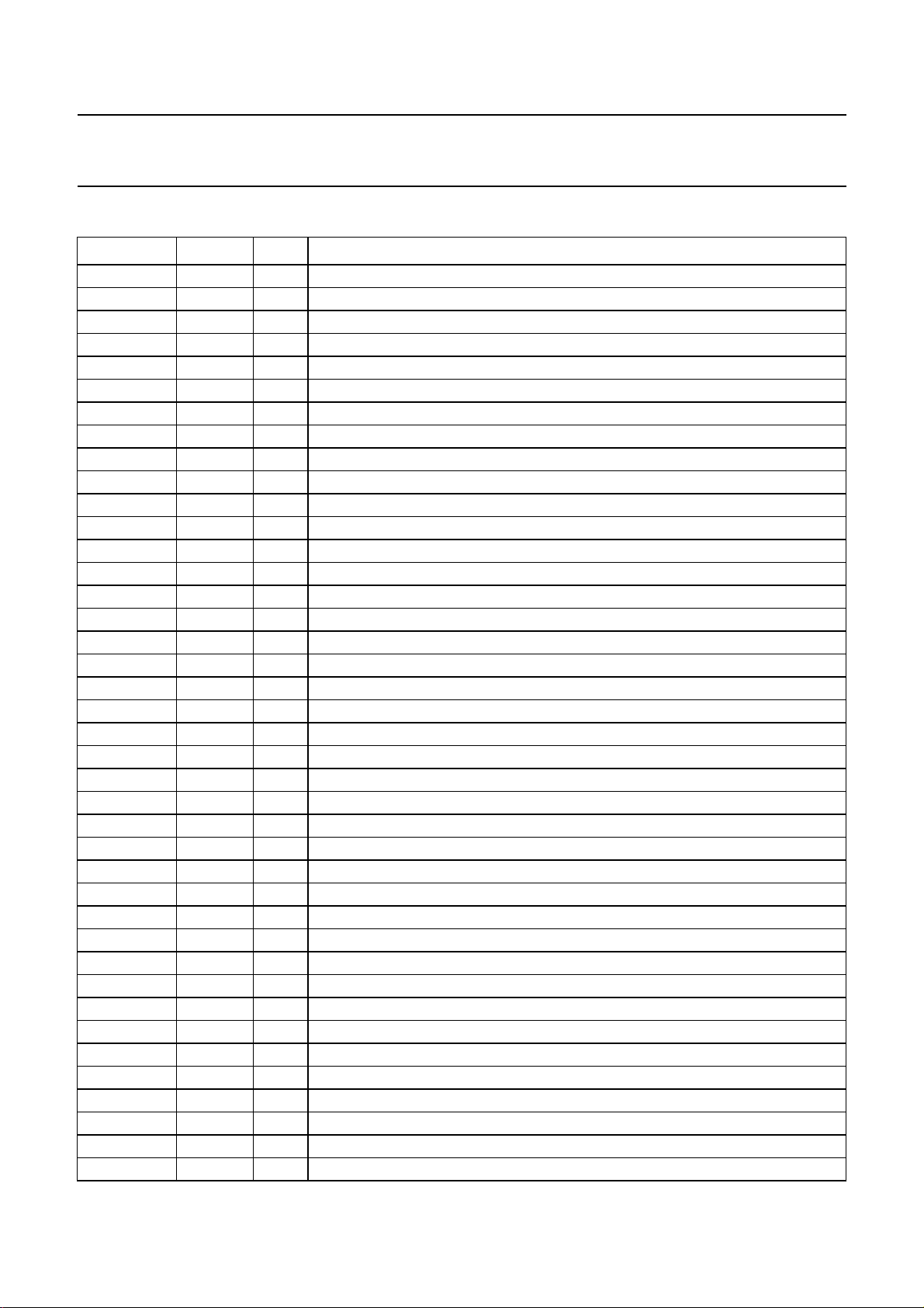
SYMBOL PIN I/O DESCRIPTION
V
ref(B)(MA)
MU 2 I analog U input for main channel
V
DDA(MF)
V
SSA(MA)
V
DDA(MA)
V
DDA(DA)
V
SSA(DA)
DY 8 O analog Y output of DAC
V
bias(DA)
DV 10 O analog V output of DAC
V
ref(T)(DA)
DU 12 O analog U output of DAC
V
ref(B)(DA)
V
DDD(DA)
V
SSD(DA)
V
SSD(P1)
V
DDD(P1)
V
SSD(T1)
V
SSD(T2)
V
DDD(RP)
n.c. 21 to 29 − not connected
V
SSD(T3)
n.c. 31 − not connected
T5 32 I/O test data input/output bit 5 (CMOS levels)
T4 33 I/O test data input/output bit 4 (CMOS levels)
T3 34 I/O test data input/output bit 3 (CMOS levels)
T2 35 I/O test data input/output bit 2 (CMOS levels)
T1 36 I/O test data input/output bit 1 (CMOS levels)
T0 37 I/O test data input/output bit 0 (CMOS levels)
TC 38 I test control input (CMOS levels)
V
DDD(RL)
V
SSD(RL)
V
SSD(RM)
V
DDD(RM)
TCLK 43 I test clock input (CMOS levels)
TM 44 I test mode input (CMOS levels)
TCBD 45 I test control block data input (CMOS levels)
TCBC 46 I test control block clock input (CMOS levels)
TCBR 47 I test control block reset input (CMOS levels)
V
SSD(T4-T7)
1 I/O analog bottom reference voltage for main channel ADCs
3 S analog supply voltage for main channel front-end buffers
4 S analog ground for main channel ADCs
5 S analog supply voltage for main channel ADCs
6 S analog supply voltage for DACs
7 S analog ground for DACs
9 I/O input/output analog bias voltage reference for DACs
11 I/O input/output analog top reference voltage for DACs
13 I/O analog bottom reference voltage for DACs
14 S digital supply voltage for DACs
15 S digital ground for DACs
16 S digital ground for periphery
17 S digital supply voltage for periphery
18 − digital ground for test
19 − digital ground for test
20 S digital supply voltage for memory periphery
30 − digital ground for test
39 S digital supply voltage for memory logic
40 S digital ground for memory logic
41 S digital ground for memory core
42 S digital supply voltage for memory core
48 to 51 − digital ground for test
1999 Feb 18 4
Philips Semiconductors Preliminary specification
NTSC Picture-In-Picture (PIP) controller SAB9082
SYMBOL PIN I/O DESCRIPTION
n.c. 52 to 60 − not connected
V
SSD(RP)
V
SSD(T8,T9)
V
DDD(P2)
V
SSD(P2)
V
SSD(D)
V
DDD(D)
FBL 68 O fast blanking control signal output (CMOS levels; +5 V tolerant)
PKOFF 69 O peak off control signal output (CMOS levels; +5 V tolerant)
DVSYNC 70 I vertical sync display channel input (CMOS levels; +5 V tolerant)
DCLK 71 I test clock input (28 MHz) (CMOS levels)
SVSYNC 72 I vertical sync for subchannel input (CMOS levels; +5 V tolerant)
SCL 73 I/O input/output serial clock (I
SDA 74 I/O input/output serial data/acknowledge output (I
POR 75 I power-on reset input (CMOS levels; pull-up resistor connected to V
V
DDA(SA)
V
SSA(SA)
V
DDA(SF)
SU 79 I analog U input for subchannel
V
ref(B)(SA)
SV 81 I analog V input for subchannel
V
ref(T)(SA)
SY 83 I analog Y input for subchannel
V
bias(SA)
V
SSD(SA)
V
DDD(SA)
SHSYNC 87 I horizontal sync input for subchannel (V
T6 88 I/O test data input/output bit 7 (CMOS levels)
V
DDA(SP)
V
SSA(SP)
V
SSA(DP)
V
DDA(DP)
T7 93 I/O test data input/output bit 6 (CMOS levels)
DHSYNC 94 I horizontal sync display input for channel (V
V
DDD(MA)
V
SSD(MA)
V
bias(MA)
MY 98 I analog Y input for main channel
V
ref(T)(MA)
MV 100 I analog V input for main channel
61 S digital ground for memory periphery
62 and 63 − digital ground for test
64 S digital supply voltage for periphery
65 S digital ground for periphery
66 S digital ground for digital core
67 S digital supply voltage for digital core
2
C-bus) (CMOS levels; +5 V tolerant)
2
C-bus) (+5 V tolerant)
76 S analog supply voltage for subchannel ADCs
77 S analog ground for subchannel ADCs
78 S analog supply voltage for subchannel front-end buffers and clamps
80 I/O input/output analog bottom reference voltage for subchannel ADCs
82 I/O input/output analog top reference voltage for subchannel ADCs
84 I/O analog bias reference voltage for subchannel ADCs
85 S digital ground for subchannel ADCs
86 S digital supply voltage for subchannel ADCs
i<VSHSYNC
)
89 S analog supply voltage for subchannel PLL
90 S analog ground for subchannel PLL
91 S analog ground for display channel PLL
92 S analog supply voltage for display channel PLL
i<VDHSYNC
)
95 S digital supply voltage for main channel ADCs
96 S digital ground for main channel ADCs
97 I/O analog bias reference voltage for main channel ADCs
99 I/O analog top reference voltage for main channel ADCs
DD
)
1999 Feb 18 5

Philips Semiconductors Preliminary specification
NTSC Picture-In-Picture (PIP) controller SAB9082
handbook, full pagewidth
ref(T)(MA)
V
ref(B)(MA)
V
DDA(MF)
V
SSA(MA)
V
DDA(MA)
V
DDA(DA)
V
SSA(DA)
V
bias(DA)
V
ref(T)(DA)
V
ref(B)(DA)
V
DDD(DA)
V
SSD(DA)
V
SSD(P1)
V
DDD(P1)
V
SSD(T1)
V
SSD(T2)
V
DDD(RP)
V
SSD(T3)
MU
DY
DV
DU
n.c.
n.c.
n.c.
n.c.
n.c.
n.c.
n.c.
n.c.
n.c.
MV
100
1
2
3
4
5
6
7
8
9
10
11
12
13
14
15
16
17
18
19
20
21
22
23
24
25
26
27
28
29
30
bias(MA)VSSD(MA)VDDD(MA)
V
MY
V
99989796959493929190898887868584838281
DDA(DP)VSSA(DP)VSSA(SP)VDDA(SP)
DHSYNCT7V
SAB9082
T6
SHSYNC
DDD(SA)VSSD(SA)Vbias(SA)
V
SY
ref(T)(SA)
V
SV
80
79
78
77
76
75
74
73
72
71
70
69
68
67
66
65
64
63
62
61
60
59
58
57
56
55
54
53
52
51
V
ref(B)(SA)
SU
V
DDA(SF)
V
SSA(SA)
V
DDA(SA)
POR
SDA
SCL
SVSYNC
DCLK
DVSYNC
PKOFF
FBL
V
DDD(D)
V
SSD(D)
V
SSD(P2)
V
DDD(P2)
V
SSD(T9)
V
SSD(T8)
V
SSD(RP)
n.c.
n.c.
n.c.
n.c.
n.c.
n.c.
n.c.
n.c.
n.c.
V
SSD(T7)
31323334353637383940414243444546474849
T5T4T3T2T1
n.c.
T0
TC
DDD(RL)
V
Fig.2 Pin configuration.
1999 Feb 18 6
SSD(RL)
SSD(RM)
V
V
TCLK
DDD(RM)
V
TM
TCBD
TCBC
TCBR
50
MGL583
SSD(T4)VSSD(T5)VSSD(T6)
V
Philips Semiconductors Preliminary specification
NTSC Picture-In-Picture (PIP) controller SAB9082
FUNCTIONAL DESCRIPTION
Acquisition
The internal pixel rate is 28 MHz for the Y, U and V channels. It is expected that the bandwidth of the input signals is
limited to 4.5 MHz for the Y input and 1.125 MHz for the U and V input. Inset synchronization is achieved via the
acquisition HSYNC and VSYNC pins of the main channel. The display is driven by the main channel clock. With the
acquisition fine positioning added to a system constant the starting point of the acquisition can be controlled. With a
nominal input HSYNC frequency, resulting in a nominal system frequency of 1792 × HSYNC (approximately 28 MHz)
and standard NTSC signals 1408 samples are acquired and processed by the SAB9082.
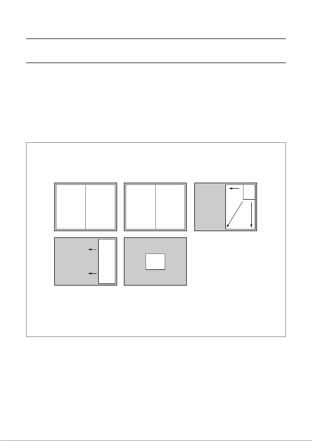
PIP modes
handbook, full pagewidth
SUB
MAIN SUB
MAIN
SUB
REPLAY
MAIN
Fig.3 PIP modes.
MGM810
1999 Feb 18 7

Philips Semiconductors Preliminary specification
NTSC Picture-In-Picture (PIP) controller SAB9082
handbook, full pagewidth
S0
S0
S0
S1
S0
S2
S4
S0
S2
S4
S0
S2
S1
S2
S1
S3
S5
MAIN
MAIN
S1
S3
S5
S1
S3
S0
S1
S2
S0
S2
S4
S1
S3
S5
MAIN
S1
S2
MAIN
MAIN
S0
S2
S4
S2
S4
S3
S5
S0
S1
S2
S1
S3
S5
MGL587
S4
S5
Fig.4 Multi PIP modes.
1999 Feb 18 8
 Loading...