

Philips SAB9080H-N1, SAB9080H-N3 Datasheet
DATA SH EET
Preliminary specification
Supersedes data of 1999 Jan 05
File under Integrated Circuits, IC02
1999 Nov 12
INTEGRATED CIRCUITS
SAB9080
NTSC Picture-In-Picture (PIP)
controller
1999 Nov 12 2
Philips Semiconductors Preliminary specification
NTSC Picture-In-Picture (PIP) controller SAB9080
FEATURES
• Double window Picture-In-Picture (PIP) in interlaced or
non-interlaced mode at 8-bit resolution
• Internal 1-Mbit DRAM
• Three 8-bit Analog-to-Digital Converters (ADCs) (7-bit
performance) with clamp circuit for each acquisition
channel
• One PLL which generatesthe line-locked clocks for the
subchannel
• One PLL which generates the line-locked clocks for the
main and display channels
• Three 8-bit Digital-to-Analog Converters (DACs)
• Linear zoom in both horizontal and vertical directions for
the subchannel
• Linear zoom in horizontal direction for the main channel.
GENERAL DESCRIPTION
The SAB9080 is an NTSC PIP controller which can be
used in double window applications. The SAB9080 inserts
oneortwolivevideosignalswithreducedsizeintoanother
live video signal. The incoming video signals are expected
to be analog baseband signals.
The conversion to the digital environment is done on chip
with ADCs. Processing and storage of the video data is
done entirely in the digital domain. The conversion back to
the analog domain is done by DACs.
Internal clocks are generated by PLLs which lock on to the
applied horizontal and vertical syncs.
The main input channel is compressed horizontally by a
factor of two and directly fed to the output. After
compression, a horizontal expansion of two is possible for
the main channel.
The subchannel is also compressed horizontally by a
factor of two but stored in memory before it is fed to the
outputs.
QUICK REFERENCE DATA
ORDERING INFORMATION
SYMBOL PARAMETER CONDITIONS MIN. TYP. MAX. UNIT
Supply
V
DDD
digital supply voltage 3.0 3.3 3.6 V
V
DDA
analog supply voltage 3.0 3.3 3.6 V
I
DDD
digital supply current − 50 − mA
I
DDA
analog supply current 140 165 210 mA
PLL
f
clk(sys)
system clock frequency 1792 × f
HSYNC
− 28 − MHz
B
loop
loop bandwidth − 4 − kHz
t
jitter
short-term stability peak-to-peak jitter for 64 µs −−4ns
ζ damping factor − 0.7 −
TYPE
NUMBER
PACKAGE
NAME DESCRIPTION VERSION
SAB9080H QFP100 plastic quad flat package; 100 leads (lead length 1.95 mm);
body 14 × 20 × 2.8 mm
SOT317-2
1999 Nov 12 3
Philips Semiconductors Preliminary specification
NTSC Picture-In-Picture (PIP) controller SAB9080
This text is here in white to force landscape pages to be rotated correctly when browsing through the pdf in the Acrobat reader.This text is here in
_white to force landscape pagesto be rotated correctly when browsing through the pdf in theAcrobat reader.This text is here inThis text is here in
white toforce landscape pages to be rotated correctly when browsingthrough the pdf inthe Acrobat reader. whiteto force landscape pagesto be ...
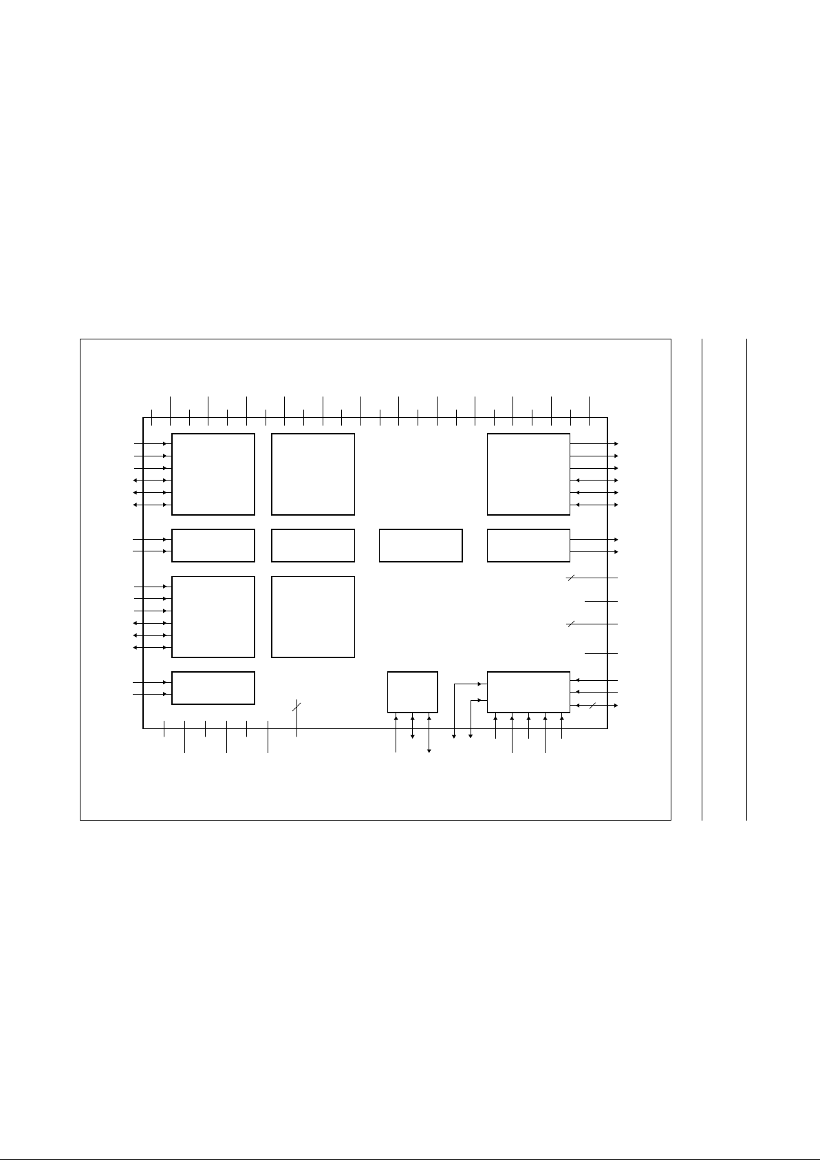
BLOCK DIAGRAM
handbook, full pagewidth
MGM808
73 88 93 44 43 45 46 47
SCL
74
SDA
T7
T6
TCLKTMTCBC
TCBD TCBR
75
POR
TEST
CONTROL
PKOFF
69
FBL
68
DAC AND BUFFER
DY
8
DV
10
DU
12
V
bias(DA)
9
V
ref(T)(DA)
11
V
ref(B)(DA)
13
SHSYNC
87
SVSYNC
72
SU
79
SV
81
SY
V
bias(SA)
V
ref(T)(SA)
V
ref(B)(SA)
83
84
82
80
DHSYNC
94
DVSYNC
70
MU
2
MY
98
MV
V
bias(MA)
V
ref(T)(MA)
V
ref(B)(MA)
100
97
99
1
PLL AND CLOCK
GENERATOR
DCLK
71
T5 to T0
32 to 37
TC
38
PLL AND CLOCK
GENERATOR
CLAMP AND ADC
CLAMP AND ADC
LINE MEMORY INTERNAL DRAM
DISPLAY
CONTROL
HORIZONTAL
AND
VERTICAL
FILTER
HORIZONTAL
FILTER
89
34
90 91 92 95
21 to 29, 31,
52 to 60
96
19
V
DDA(MF)
V
SSA(MA)
56
V
DDA(MA)
V
DDA(DA)
714
V
SSA(DA)
V
DDD(DA)
15 16
V
SSD(DA)
V
SSD(P1)
17 20
V
DDD(P1)
V
DDD(RP)
39 40
V
DDD(RL)
V
SSD(RL)
41 42
V
SSD(RM)
V
DDD(RM)
61 64
V
SSD(RP)
V
DDD(P2)
65 66
V
SSD(P2)
V
SSD(D)
67 76
V
DDD(D)
V
DDA(SA)
77 78
V
SSA(SA)
V
DDA(SF)
85 86
V
SSD(SA)
V
DDD(SA)
SAB9080
V
SSD(MA)
V
DDD(MA)
n.c.
V
DDA(DP)
V
SSA(DP)
V
SSA(SP)
V
DDA(SP)
I
2
C-BUS
CONTROL
6
V
SSD(T1)
and
V
SSD(T2)
V
SSD(T4)
to
V
SSD(T7)
V
SSD(T8)
and
V
SSD(T9)
18, 19
48 to 51
62, 63
V
SSD(T3)
30
4
2
Fig.1 Block diagram.
1999 Nov 12 4
Philips Semiconductors Preliminary specification
NTSC Picture-In-Picture (PIP) controller SAB9080
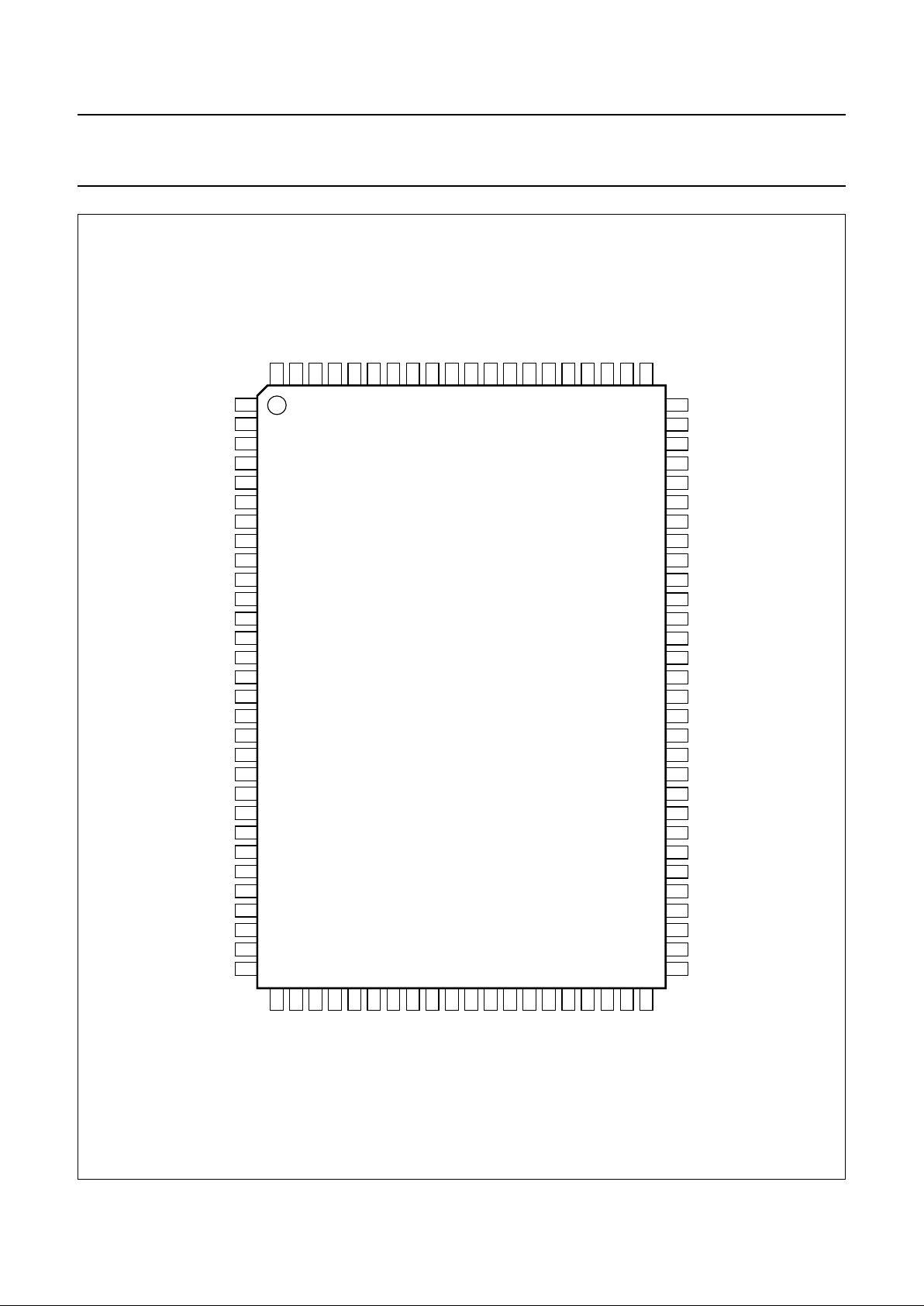
PINNING
SYMBOL PIN TYPE DESCRIPTION
V
ref(B)(MA)
1 I/O analog bottom reference voltage for main channel ADCs
MU 2 I analog U input for main channel
V
DDA(MF)
3 S analog supply voltage for main channel front-end buffers
V
SSA(MA)
4 S analog ground for main channel ADCs
V
DDA(MA)
5 S analog supply voltage for main channel ADCs
V
DDA(DA)
6 S analog supply voltage for DACs
V
SSA(DA)
7 S analog ground for DACs
DY 8 O analog Youtput of DAC
V
bias(DA)
9 I/O input/output analog bias reference voltage for DACs
DV 10 O analog Voutput of DAC
V
ref(T)(DA)
11 I/O input/output analog top reference voltage for DACs
DU 12 O analog U output of DAC
V
ref(B)(DA)
13 I/O analog bottom reference voltage for DACs
V
DDD(DA)
14 S digital supply voltage for DACs
V
SSD(DA)
15 S digital ground for DACs
V
SSD(P1)
16 S digital ground for periphery
V
DDD(P1)
17 S digital supply voltage for periphery
V
SSD(T1)
18 S digital ground for test
V
SSD(T2)
19 S digital ground for test
V
DDD(RP)
20 S digital supply voltage for memory periphery
n.c. 21 to 29 − not connected
V
SSD(T3)
30 S digital ground for test
n.c. 31 − not connected
T5 32 I/O test data input/output bit 5 (CMOS levels)
T4 33 I/O test data input/output bit 4 (CMOS levels)
T3 34 I/O test data input/output bit 3 (CMOS levels)
T2 35 I/O test data input/output bit 2 (CMOS levels)
T1 36 I/O test data input/output bit 1 (CMOS levels)
T0 37 I/O test data input/output bit 0 (CMOS levels)
TC 38 I test control input (CMOS levels)
V
DDD(RL)
39 S digital supply voltage for memory logic
V
SSD(RL)
40 S digital ground for memory logic
V
SSD(RM)
41 S digital ground for memory core
V
DDD(RM)
42 S digital supply voltage for memory core
TCLK 43 I test clock input (CMOS levels)
TM 44 I test mode input (CMOS levels)
TCBD 45 I test control block data input (CMOS levels)
TCBC 46 I test control block clock input (CMOS levels)
TCBR 47 I test control block reset input (CMOS levels)
V
SSD(T4) toVSSD(T7)
48 to 51 S digital ground for test
1999 Nov 12 5
Philips Semiconductors Preliminary specification
NTSC Picture-In-Picture (PIP) controller SAB9080
n.c. 52 to 60 − not connected
V
SSD(RP)
61 S digital ground for memory periphery
V
SSD(T8)
and V
SSD(T9)
62 and 63 S digital ground for test
V
DDD(P2)
64 S digital supply voltage for periphery
V
SSD(P2)
65 S digital ground for periphery
V
SSD(D)
66 S digital ground for digital core
V
DDD(D)
67 S digital supply voltage for digital core
FBL 68 O fast blanking control signal output (CMOS levels; +5 V tolerant)
PKOFF 69 O peak off control signal output (CMOS levels; +5 V tolerant)
DVSYNC 70 I vertical sync display channel input (CMOS levels; +5 V tolerant)
DCLK 71 I test clock input (28 MHz; CMOS levels)
SVSYNC 72 I vertical sync for subchannel input (CMOS levels; +5 V tolerant)
SCL 73 I/O input/output serial clock (I
2
C-bus; CMOS levels; +5 V tolerant)
SDA 74 I/O input/output serial data/acknowledge output (I
2
C-bus; +5 V tolerant)
POR 75 I power-on reset input (CMOS levels; pull-up resistor connected to V
DD
)
V
DDA(SA)
76 S analog supply voltage for subchannel ADCs
V
SSA(SA)
77 S analog ground for subchannel ADCs
V
DDA(SF)
78 S analog supply voltage for subchannel front-end buffers and clamps
SU 79 I analog U input for subchannel
V
ref(B)(SA)
80 I/O input/output analog bottom reference voltage for subchannel ADCs
SV 81 I analog V input for subchannel
V
ref(T)(SA)
82 I/O input/output analog top reference voltage for subchannel ADCs
SY 83 I analog Y input for subchannel
V
bias(SA)
84 I/O analog bias reference voltage for subchannel ADCs
V
SSD(SA)
85 S digital ground for subchannel ADCs
V
DDD(SA)
86 S digital supply voltage for subchannel ADCs
SHSYNC 87 I horizontal sync input for subchannel (V
i<VSHSYNC
)
T6 88 I/O test data input/output bit 7 (CMOS levels)
V
DDA(SP)
89 S analog supply voltage for subchannel PLL
V
SSA(SP)
90 S analog ground for subchannel PLL
V
SSA(DP)
91 S analog ground for display channel PLL
V
DDA(DP)
92 S analog supply voltage for display channel PLL
T7 93 I/O test data input/output bit 6 (CMOS levels)
DHSYNC 94 I horizontal sync input for display channel (V
i<VDHSYNC
)
V
DDD(MA)
95 S digital supply voltage for main channel ADCs
V
SSD(MA)
96 S digital ground for main channel ADCs
V
bias(MA)
97 I/O analog bias reference voltage for main channel ADCs
MY 98 I analog Y input for main channel
V
ref(T)(MA)
99 I/O analog top reference voltage for main channel ADCs
MV 100 I analog V input for main channel
SYMBOL PIN TYPE DESCRIPTION
1999 Nov 12 6
Philips Semiconductors Preliminary specification
NTSC Picture-In-Picture (PIP) controller SAB9080
Fig.2 Pin configuration.
handbook, full pagewidth
80
79
78
77
76
75
74
73
72
71
70
69
68
67
66
65
64
63
62
61
60
59
58
57
56
55
54
53
52
51
V
ref(B)(SA)
SU
V
DDA(SF)
V
SSA(SA)
V
DDA(SA)
POR
SDA
SCL
SVSYNC
DCLK
DVSYNC
PKOFF
FBL
V
DDD(D)
V
SSD(D)
V
SSD(P2)
V
DDD(P2)
V
SSD(RP)
V
SSD(T9)
V
SSD(T8)
V
SSD(T7)
n.c.
n.c.
n.c.
n.c.
n.c.
n.c.
n.c.
n.c.
n.c.
V
ref(B)(MA)
MU
V
DDA(MF)
V
SSA(MA)
V
DDA(MA)
V
DDA(DA)
V
SSA(DA)
DY
V
bias(DA)
DV
V
ref(T)(DA)
DU
V
ref(B)(DA)
V
DDD(DA)
V
SSD(DA)
V
SSD(P1)
V
SSD(T3)
n.c.
V
DDD(P1)
V
SSD(T1)
V
SSD(T2)
V
DDD(RP)
n.c.
n.c.
n.c.
n.c.
n.c.
n.c.
n.c.
n.c.
T5T4T3T2T1
T0
TC
V
DDD(RL)
V
SSD(RL)
n.c.
V
SSD(T4)VSSD(T5)VSSD(T6)
V
SSD(RM)
V
DDD(RM)
TCLK
TM
TCBD
TCBC
TCBR
MV
V
ref(T)(MA)
MY
V
bias(MA)VSSD(MA)VDDD(MA)
DHSYNCT7V
DDA(DP)VSSA(DP)VSSA(SP)VDDA(SP)
T6
SHSYNC
V
DDD(SA)VSSD(SA)Vbias(SA)
SY
V
ref(T)(SA)
SV
30
29
28
27
26
25
24
23
22
21
20
19
18
17
16
15
14
13
12
11
10
9
8
7
6
5
4
3
2
1
100
99989796959493929190898887868584838281
31323334353637383940414243444546474849
50
MGM809
SAB9080

1999 Nov 12 7
Philips Semiconductors Preliminary specification
NTSC Picture-In-Picture (PIP) controller SAB9080
FUNCTIONAL DESCRIPTION
Acquisition
The internal pixel rate is 28 MHz for the Y, U and V
channels. It is expected that the bandwidth of the input
signals will be limited to 4.5 MHz for the Y input and
1.125 MHzfortheU and V inputs.Inset synchronisation is
achieved via the acquisition HSYNC and VSYNC pins of
the main channel. The display is driven by the main
channel clock.
The starting-point of the acquisition can be controlled with
the acquisition fine positioning added to a system
constant. With a nominal input 1792 × f
HSYNC
and
standard NTSC signals, 1408 samples (active video) are
acquired and processed by the SAB9080. Here, the
nominal input f
HSYNC
results in a nominal system clock
frequency of 1792 × f
HSYNC
(approximately 28 MHz).
PIP modes
Fig.3 PIP modes.
handbook, full pagewidth
MGM810
MAIN
REPLAY
MAIN SUB
SUB
MAIN
SUB
I2C-bus description
The I2C-bus provides bidirectional 2-line communication
between different ICs. The SDA line is the serial data line
and the SCL the serial clock line. Both lines must be
connected to a positive supply via a pull-up resistor when
connected to the output stages of a device.
Data transfer may be initiated only when the bus is not
busy. The SAB9080 has the I2C-bus address 2CH. Valid
subaddresses are 00H to 18H; registers 15H to 18H are
reserved for future extensions.
I
2
C-bus control is according to the I2C-bus protocol: first, a
START sequence must be put on the I2C-bus. Then, the
I2C-bus address of the circuit must be sent, followed by a
subaddress. After this sequence, the data of the
subaddresses must be sent. An auto-increment function
gives the option of sending data of the incremented
subaddresses until a STOP sequence is sent. Table 1
gives an overview of the I2C-bus addresses. The data bits
that are not used should be set to zero.
1999 Nov 12 8
Philips Semiconductors Preliminary specification
NTSC Picture-In-Picture (PIP) controller SAB9080
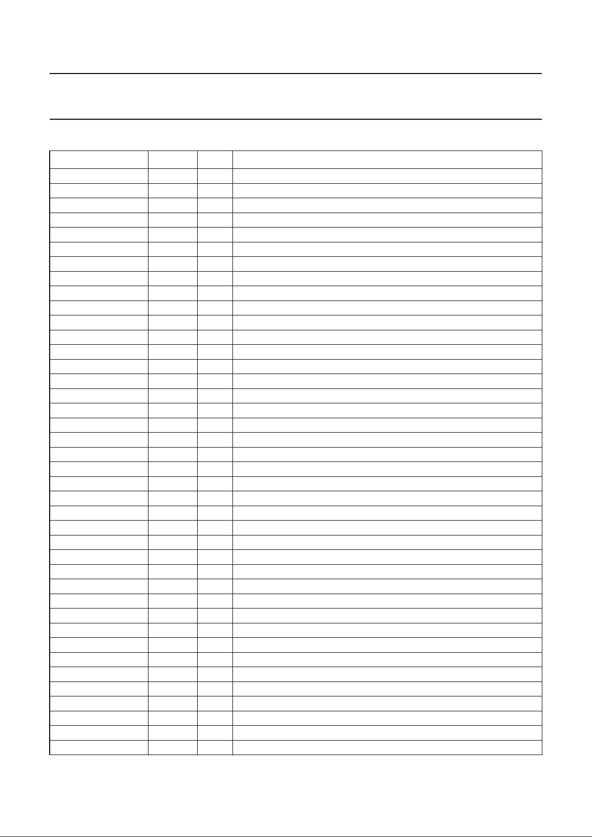
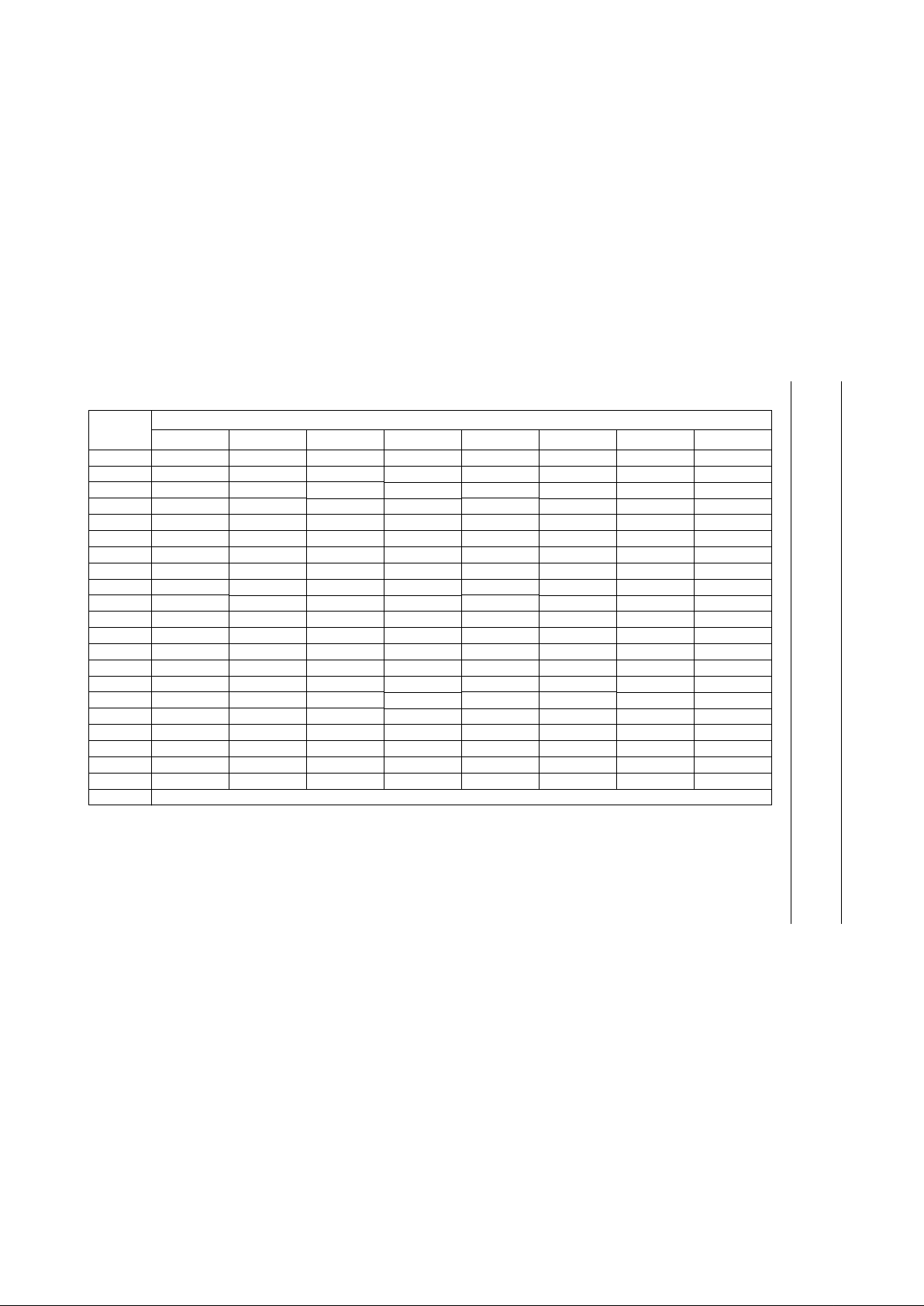
Table 1 Overview of I2C-bus addresses
For a description of the various data bits, see the following pages.
SUB-
ADDRESS
DATA BYTES
BIT 7 BIT 6 BIT 5 BIT 4 BIT 3 BIT 2 BIT 1 BIT 0
00H MPIPON SPIPON S1FLD SFreeze DNonint PipMode2 PipMode1 PipMode0
01H SHBlow1 SHBlow0 SHRed5 SHRed4 SHRed3 SHRed2 SHRed1 SHRed0
02H SVBlow SVRed6 SVRed5 SVRed4 SVRed3 SVRed2 SVRed1 SVRed0
03H BGVfp3 BGVfp2 BGVfp1 BGVfp0 BGHfp3 BGHfp2 BGHfp1 BGHfp0
04H SDHfp7 SDHfp6 SDHfp5 SDHfp4 SDHfp3 SDHfp2 SDHfp1 SDHfp0
05H SDVfp7 SDVfp6 SDVfp5 SDVfp4 SDVfp3 SDVfp2 SDVfp1 SDVfp0
06H −−−−−−−−
07H −−−−−−−−
08H MAHfp3 MAHfp2 MAHfp1 MAHfp0 SAHfp3 SAHfp2 SAHfp1 SAHfp0
09H SAVfp7 SAVfp6 SAVfp5 SAVfp4 SAVfp3 SAVfp2 SAVfp1 SAVfp0
0AH DUVPol DVSPol DFPol DHsync SUVPol SVSPol SFPol SHsync
0BH MainFidPos7 MainFidPos6 MainFidPos5 MainFidPos4 MainFidPos3 MainFidPos2 MainFidPos1 MainFidPos0
0CH SubFidPos7 SubFidPos6 SubFidPos5 SubFidPos4 SubFidPos3 SubFidPos2 SubFidPos1 SubFidPos0
0DH BGOn BOn MFidPOn SFidPOn Prio AlgOff SFBlkPkOff1 SFBlkPkOff0
0EH BSel1 BSel0 SBBrt1 SBBrt0 − SBCol2 SBCol1 SBCol0
0FH −−SLSel5 SLSel4 SLSel3 SLSel2 SLSel1 SLSel0
10H I2CHold SV1 SDSel5 SDSel4 SDSel3 SDSel2 SDSel1 SDSel0
11H MDHfp7 MDHfp6 MDHfp5 MDHfp4 MDHfp3 MDHfp2 MDHfp1 MDHfp0
12H MDVfp7 MDVfp6 MDVfp5 MDVfp4 MDVfp3 MDVfp2 MDVfp1 MDVfp0
13H MHBlow SV2 MHRed5 MHRed4 MHRed3 MHRed2 MHRed1 MHRed0
14H − VBwidth2 VBwidth1 VBwidth0 − HBwidth2 HBwidth1 HBwidth0
15H to 18H all bits are reserved
 Loading...