

Philips SAB9079HS Datasheet
INTEGRATED CIRCUITS
DATA SH EET
SAB9079HS
Multistandard Picture-In-Picture
(PIP) controller
Preliminary specification
File under Integrated Circuits, IC02
2000 Jan 13
Philips Semiconductors Preliminary specification
Multistandard Picture-In-Picture (PIP)
controller
FEATURES
• Suitable for single PIP, double window and multi PIP
applications
• Data formats 4 : 1 : 1 (all modes) and 4:2:2(most
modes)
• Sample rate of 14 MHz, 720 Y*-pixels/line
• Horizontal reduction factors1⁄
• Vertical reduction factors1⁄1,1⁄2,1⁄3and1⁄
• PIP OSD for the sub channels displayed
• Detection of PAL/NTSC with overrule bit
• CTE/LTE like circuits in display part
• Replay with definable auto increment, picture sample
rate and picture number auto wrap
• Programmable Y*UV to RGB conversion matrix with
independent coefficients for NTSC and PAL sources
• Display clock and synchronisation are derived from the
main PLL
• Three 8-bit Digital-to-Analog Converters (DACs)
• Three 8-bit Analog-to-Digital Converters (ADCs)
(7-bit performance) with clamp circuit for each
acquisition channel
• Main and sub can write to the same VDRAM address
spaces under certain conditions; the reduction factors
should be the same
• Y* and UV pedestals on the acquisition sides
• Independent vertical filtering with 1 : 1 for UV and Y* at
the display part.
3
⁄4,2⁄3,1⁄2,1⁄3,1⁄4and1⁄
1
4
SAB9079HS
GENERAL DESCRIPTION
6
The SAB9079HS is a PIP controller for a multistandard
application environment in combination with a
multistandard decoder such as for example TDA8310,
TDA9143 or TDA9321H.
The SAB9079HSinserts one or two live video signals with
reduced sizes into the main/display video signal. All video
signals are expected to be analog baseband signals. The
analog signals are stripped signals without sync.
Therefore the luminance signal is referred to as Y*. The
conversion into the digital environment and back is done
on-chip as well as the internal clock generation.
The SAB9079HS is suitablefor single PIP, double window
and multi PIP applications.
ORDERING INFORMATION
TYPE
NUMBER
SAB9079HS SQFP128 plastic shrink quad flat package; 128 leads (lead length 1.6 mm);
2000 Jan 13 2
NAME DESCRIPTION VERSION
body 14 × 20 × 2.72 mm
PACKAGE
SOT387-3

Philips Semiconductors Preliminary specification
Multistandard Picture-In-Picture (PIP)
SAB9079HS
controller
QUICK REFERENCE DATA
SYMBOL PARAMETER CONDITIONS MIN. TYP. MAX. UNIT
Supplies
V
DDD(C)
V
DDD(P)
V
DDA
I
DDD(C)
I
DDD(P)
I
DDA
PLL
f
osc
f
sys
B
loop
t
jitter
ζ damping factor − 0.7 −
digital supply voltage for the core 3.0 3.3 3.6 V
digital supply voltage for the
4.5 5.0 5.5 V
periphery
analog supply voltage 3.0 3.3 3.6 V
digital supply current for the core tbf 115 tbf mA
digital supply current for the
tbf 10 tbf mA
periphery
analog supply current − 170 210 mA
oscillator frequency 3584 × HSYNC − 56 − MHz
system frequency 1792 × HSYNC − 28 − MHz
896 × HSYNC − 14 − MHz
448 × HSYNC − 7 − MHz
loop bandwidth − 4 − kHz
short term stability jitter during 64 µs −−4ns
2000 Jan 13 3

This text is here in white to force landscape pages to be rotated correctly when browsing through the pdf in the Acrobat reader.This text is here in
_white to force landscape pages to be rotated correctly when browsing through the pdf in the Acrobat reader.This text is here inThis text is here in
white to force landscape pages to be rotated correctly when browsing through the pdf in the Acrobat reader. white to force landscape pages to be ...
2000 Jan 13 4
handbook, full pagewidth
BLOCK DIAGRAM
Philips Semiconductors Preliminary specification
Multistandard Picture-In-Picture (PIP)
controller
V
bias(SA)
V
ref(T)(SA)
V
ref(B)(SA)
SHSYNC
SVSYNC
V
bias(MA)
V
ref(T)(MA)
V
ref(B)(MA)
MHSYNC
MVSYNC
V
DDA(MF)
SY
SU
SV
MY
MU
MV
V
SSA(MA)
1
105
103
101
104
107
106
94
95
126
128
2
127
124
125
9
8
V
DDA(MA)
V
V
DDA(MP)
3
4
CLAMP AND ADC
PLL AND CLOCK
GENERATOR
CLAMP AND ADC
PLL AND CLOCK
GENERATOR
V
DDA(MH)
SSA(MP)
10
11
V
V
DDA(SA)
12
V
DDA(SF)
SSA(SA)
99
100
HORIZONTAL
VERTICAL
LINE MEMORY
HORIZONTAL
VERTICAL
LINE MEMORY
V
DDA(SH)
102
AND
FILTER
AND
FILTER
V
SSA(SP)
91
V
DDA(SP)
92
93
RAS
78
CAS
WE
70 77 40 51
TEST
CONTROL
AD8
DT
to AD0
SC
79 to 83,
74 to 71
VDRAM CONTROL
AND
(RE-)FORMATTING
SAB9079HS
I2C-BUS
CONTROL
DAO0
to DAO15
41 to 46,
49, 50, 69,
67, 65, 61,
59, 57, 55, 53
DAI0
to DAI15
39 to 32,
68, 66, 64,
60, 58, 56,
54, 52
V
DDA(DA)
V
SSA(DA)
30
DAC
AND
BUFFER
DISPLAY
CONTROL
LINE MEMORY
PLL AND CLOCK
GENERATOR
V
DDD(P)
31
113
24
DY
27
DU
29
DV
28
V
bias(DA)
26
V
ref(B)(DA)
25
V
ref(T)(DA)
19
DFB
84
n.c.
21
DVSYNC
20
DHSYNC
V
DDD(C1)
to
V
DDD(C7)
15, 18, 22,
85, 88,
109, 122
V
V
16, 17, 23,
86, 87,
108, 123
SSD(C1)
to
SSD(C7)
V
SSD(P1)
to
V
SSD(P5)
13,
47, 63,
75, 90
V
DDD(P1)
to
V
DDD(P5)
14,
48, 62,
76, 89
98
TSEXT
111 114
TCBD
TCBR A0
TCBC SCL
Fig.1 Block diagram.
97112 116
110 115
TSMSB POR
SDA
117
TMMSB
6
TMEXT
5
TSCLK
121
96
120
TM0
TM2
TM1
119
118
TC
7
TMCLK
MGS386
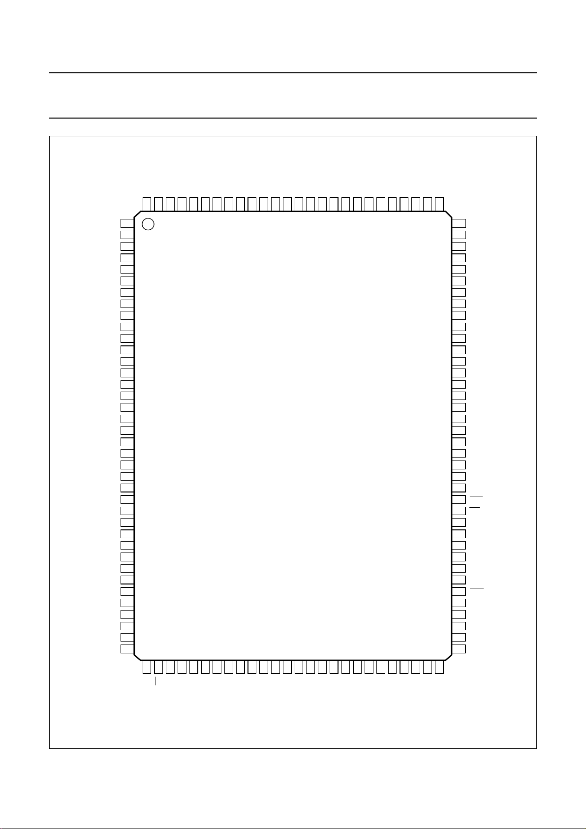
SAB9079HS

Philips Semiconductors Preliminary specification
Multistandard Picture-In-Picture (PIP)
SAB9079HS
controller
PINNING
SYMBOL PIN I/O DESCRIPTION
V
DDA(MF)
MV 2 I analog V input of main channel
V
SSA(MA)
V
DDA(MA)
TMEXT 5 I set main PLL input for external mode (CMOS levels)
TMMSB 6 O test main MSB output of PLL counter (CMOS levels)
TMCLK 7 I test clock main input (CMOS levels)
MVSYNC 8 I vertical sync input for main channel (CMOS levels with hysteresis)
MHSYNC 9 I horizontal sync input for main channel (CMOS levels with hysteresis)
V
DDA(MP)
V
SSA(MP)
V
DDA(MH)
V
SSD(P1)
V
DDD(P1)
V
DDD(C1)
V
SSD(C1)
V
SSD(C2)
V
DDD(C2)
DFB 19 O fast blanking control output (CMOS levels)
DHSYNC 20 O horizontal sync output (CMOS levels)
DVSYNC 21 O vertical sync output (CMOS levels)
V
DDD(C3)
V
SSD(C3)
DY 24 O analog Y* output of DAC
V
ref(T)(DA)
V
ref(B)(DA)
DU 27 O analog U output of DAC
V
bias(DA)
DV 29 O analog Voutput of DAC
V
SSA(DA)
V
DDA(DA)
DAI7 32 I memory input data bit 7 (CMOS levels)
DAI6 33 I memory input data bit 6 (CMOS levels)
DAI5 34 I memory input data bit 5 (CMOS levels)
DAI4 35 I memory input data bit 4 (CMOS levels)
DAI3 36 I memory input data bit 3 (CMOS levels)
DAI2 37 I memory input data bit 2 (CMOS levels)
DAI1 38 I memory input data bit 1 (CMOS levels)
DAI0 39 I memory input data bit 0 (CMOS levels)
DT 40 O memory data transfer (CMOS levels)
1 S analog supply voltage for main channel front-end (3.3 V)
3 S analog ground for main channel ADCs
4 S analog supply voltage for main channel ADCs (3.3 V)
10 S analog supply voltage for main channel PLL (3.3 V)
11 S analog ground for main channel PLL
12 S supply of main HSYNC input (5.0 V)
13 S digital ground 1 for periphery; note 1
14 S digital supply voltage 1 for periphery (5.0 V); note 2
15 S digital supply voltage 1 for core (3.3 V); note 3
16 S digital ground 1 for core; note 4
17 S digital ground 2 for core; note 4
18 S digital supply voltage 2 for core (3.3 V); note 3
22 S digital supply voltage 3 for core (3.3 V); note 3
23 S digital ground 3 for core; note 4
25 I/O analog top reference for DACs
26 I/O analog bottom reference for DACs
28 I/O analog voltage reference DACs
30 S analog ground for DACs
31 S analog supply voltage for DACs (3.3 V)
2000 Jan 13 5

Philips Semiconductors Preliminary specification
Multistandard Picture-In-Picture (PIP)
controller
SYMBOL PIN I/O DESCRIPTION
DAO0 41 O memory output data bit 0 (CMOS levels)
DAO1 42 O memory output data bit 1 (CMOS levels)
DAO2 43 O memory output data bit 2 (CMOS levels)
DAO3 44 O memory output data bit 3 (CMOS levels)
DAO4 45 O memory output data bit 4 (CMOS levels)
DAO5 46 O memory output data bit 5 (CMOS levels)
V
SSD(P2)
V
DDD(P2)
DAO6 49 O memory output data bit 6 (CMOS levels)
DAO7 50 O memory output data bit 7 (CMOS levels)
SC 51 O memory shift clock output (CMOS levels)
DAI15 52 I memory input data bit 15 (CMOS levels)
DAO15 53 O memory output data bit 15 (CMOS levels)
DAI14 54 I memory input data bit 14 (CMOS levels)
DAO14 55 O memory output data bit 14 (CMOS levels)
DAI13 56 I memory input data bit 13 (CMOS levels)
DAO13 57 O memory output data bit 13 (CMOS levels)
DAI12 58 I memory input data bit 12 (CMOS levels)
DAO12 59 O memory output data bit 12 (CMOS levels)
DAI11 60 I memory input data bit 11 (CMOS levels)
DAO11 61 O memory output data bit 11 (CMOS levels)
V
DDD(P3)
V
SSD(P3)
DAI10 64 I memory input data bit 10 (CMOS levels)
DAO10 65 O memory output data bit 10 (CMOS levels)
DAI9 66 I memory input data bit 9 (CMOS levels)
DAO9 67 O memory output data bit 9 (CMOS levels)
DAI8 68 I memory input data bit 8 (CMOS levels)
DAO8 69 O memory output data bit 8 (CMOS levels)
CAS 70 O memory column address strobe output (CMOS levels)
AD0 71 O memory address output bit 0 (CMOS levels)
AD1 72 O memory address output bit 1 (CMOS levels)
AD2 73 O memory address output bit 2 (CMOS levels)
AD3 74 O memory address output bit 3 (CMOS levels)
V
SSD(P4)
V
DDD(P4)
WE 77 O memory write enable output (CMOS levels)
RAS 78 O memory row address strobe output (CMOS levels)
AD8 79 O memory address output bit 8 (CMOS levels)
AD7 80 O memory address output bit 7 (CMOS levels)
AD6 81 O memory address output bit 6 (CMOS levels)
47 S digital ground 2 for periphery; note 1
48 S digital supply voltage 2 for periphery (5.0 V); note 2
62 S digital supply voltage 3 for periphery (5.0 V); note 2
63 S digital ground 3 for periphery; note 1
75 S digital ground 4 for periphery; note 1
76 S digital supply voltage 4 for periphery (5.0 V); note 2
SAB9079HS
2000 Jan 13 6

Philips Semiconductors Preliminary specification
Multistandard Picture-In-Picture (PIP)
SAB9079HS
controller
SYMBOL PIN I/O DESCRIPTION
AD5 82 O memory address output bit 5 (CMOS levels)
AD4 83 O memory address output bit 4 (CMOS levels)
n.c. 84 − not used in application
V
DDD(C4)
V
SSD(C4)
V
SSD(C5)
V
DDD(C5)
V
DDD(P5)
V
SSD(P5)
V
DDA(SH)
V
SSA(SP)
V
DDA(SP)
SHSYNC 94 I horizontal sync input for sub channel (CMOS levels with hysteresis)
SVSYNC 95 I vertical sync input for sub channel (CMOS levels with hysteresis)
TSCLK 96 I test clock input for sub (CMOS levels)
TSMSB 97 O test sub MSB output for PLL counter (CMOS levels)
TSEXT 98 I set sub PLL input for external mode (CMOS levels)
V
DDA(SA)
V
SSA(SA)
SV 101 I analog V input of sub channel
V
DDA(SF)
SU 103 I analog U input of sub channel
V
bias(SA)
SY 105 I analog Y* input of sub channel
V
ref(B)(SA)
V
ref(T)(SA)
V
SSD(C6)
V
DDD(C6)
TCBC 110 I test control block clock input (CMOS levels)
TCBD 111 I test control block data input (CMOS levels)
TCBR 112 I test control block reset input (CMOS levels)
V
DDD(P)
A0 114 I address select pin input (I
SDA 115 I/O serial input data/ACK output (I
SCL 116 I serial clock input (I
POR 117 I power-on reset input (CMOS levels with hysteresis and pull-up resistor to V
TC 118 I test control input (CMOS levels)
TM1 119 I/O test mode input/output (CMOS levels with hysteresis and pull-up resistor to V
TM2 120 I/O test mode input/output (CMOS levels with hysteresis and pull-up resistor to V
TM0 121 I test mode input (CMOS levels)
V
DDD(C7)
85 S digital supply voltage 4 for core (3.3 V); note 3
86 S digital ground 4 for core; note 4
87 S digital ground 5 for core; note 4
88 S digital supply voltage 5 for core (3.3 V); note 3
89 S digital supply voltage 5 for periphery (5.0 V); note 2
90 S digital ground 5 for periphery; note 1
91 S supply of sub HSYNC input (5.0 V)
92 S analog ground for sub channel PLL
93 S analog supply voltage for sub channel PLL (3.3 V)
99 S analog supply voltage for sub channel ADCs (3.3 V)
100 S analog ground for sub channel ADCs
102 S analog supply voltage for sub channel frontend (3.3 V)
104 I/O analog bias reference input for sub channel ADCs
106 I/O analog bottom reference for sub channel ADCs
107 I/O analog top reference for sub channel ADCs
108 S digital ground 6 for core; note 4
109 S digital supply voltage 6 for core (3.3 V); note 3
113 S digital supply voltage for periphery (5.0 V); note 5
2
C-bus) (CMOS levels)
2
C-bus) (CMOS input levels)
2
C-bus) (CMOS levels)
122 S digital supply voltage 7 for core (3.3 V); note 3
DD
DD
DD
)
)
)
2000 Jan 13 7

Philips Semiconductors Preliminary specification
Multistandard Picture-In-Picture (PIP)
controller
SYMBOL PIN I/O DESCRIPTION
V
SSD(C7)
V
ref(T)(MA)
V
ref(B)(MA)
MY 126 I analog Y* input for main channel
V
bias(MA)
MU 128 I analog U input for main channel
Notes
1. All periphery V
2. All periphery V
3. All core V
4. All core V
5. This pin is NOT connected to the other periphery V
123 S digital ground 7 for core; note 4
124 I/O analog top reference for main channel ADCs
125 I/O analog bottom reference for main channel ADCs
127 I/O analog bias reference for main channel ADCs
are internally connected to each other, unless otherwise specified.
SS(P)
are internally connected to each other, unless otherwise specified.
DD(P)
are internally connected to each other.
DD(C)
are internally connected to each other.
SS(C)
.
DD(P)
SAB9079HS
2000 Jan 13 8
Philips Semiconductors Preliminary specification
Multistandard Picture-In-Picture (PIP)
controller
handbook, full pagewidth
bias(MA)
ref(B)(MA)
ref(T)(MA)
V
125
SSD(C7)VDDD(C7)
V
V
124
123
122
TM0
121
TM2
TM1TCPOR
120
119
118
V
DDA(MF)
V
SSA(MA)
V
DDA(MA)
TMEXT
TMMSB
TMCLK
MVSYNC
MHSYNC
V
DDA(MP)
V
SSA(MP)
V
DDA(MH)
V
SSD(P1)
V
DDD(P1)
V
DDD(C1)
V
SSD(C1)
V
SSD(C2)
V
DDD(C2)
DHSYNC
DVSYNC
V
DDD(C3)
V
SSD(C3)
V
ref(T)(DA)
V
ref(B)(DA)
V
bias(DA)
V
SSA(DA)
V
DDA(DA)
MV
DFB
DY
DU
DV
DAI7
DAI6
DAI5
DAI4
DAI3
DAI2
DAI1
V
MU
MY
127
128
126
1
2
3
4
5
6
7
8
9
10
11
12
13
14
15
16
17
18
19
20
21
22
23
24
25
26
27
28
29
30
31
32
33
34
35
36
37
38
SCL
SDAA0V
117
116
115
SAB9079HS
114
DDD(P)
TCBR
113
112
TCBD
111
DDD(C6)VSSD(C6)Vref(T)(SA)Vref(B)(SA)
TCBC
V
110
109
108
107
106
SAB9079HS
bias(SA)
SY
V
SU
105
104
103
102
101
100
99
98
97
96
95
94
93
92
91
90
89
88
87
86
85
84
83
82
81
80
79
78
77
76
75
74
73
72
71
70
69
68
67
66
65
V
DDA(SF)
SV
V
SSA(SA)
V
DDA(SA)
TSEXT
TSMSB
TSCLK
SVSYNC
SHSYNC
V
DDA(SP)
V
SSA(SP)
V
DDA(SH)
V
SSD(P5)
V
DDD(P5)
V
DDD(C5)
V
SSD(C5)
V
SSD(C4)
V
DDD(C4)
n.c.
AD4
AD5
AD6
AD7
AD8
RAS
WE
V
DDD(P4)
V
SSD(P4)
AD3
AD2
AD1
AD0
CAS
DAO8
DAI8
DAO9
DAI9
DAO10
40394142434445464748495051525354555657585960616263
DT
DAI0
DAO0
DAO1
DAO2
DAO3
DAO4
DAO5
SSD(P2)
DDD(P2)
V
V
DAO6
DAO7
Fig.2 Pin configuration.
2000 Jan 13 9
SC
DAI15
DAO15
DAI14
DAO14
DAI13
DAO13
DAI12
DAI11
DAO12
DAO11
DDD(P3)
V
64
DAI10
SSD(P3)
V
MGS387
Philips Semiconductors Preliminary specification
Multistandard Picture-In-Picture (PIP)
SAB9079HS
controller
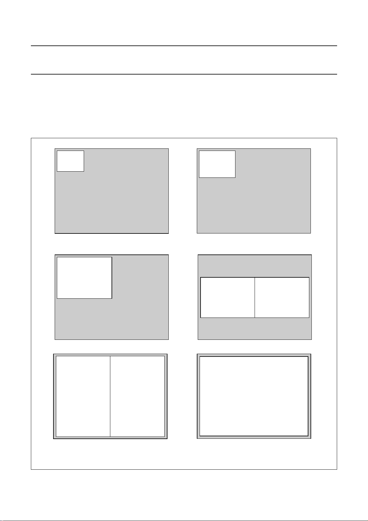
SYSTEM DESCRIPTION
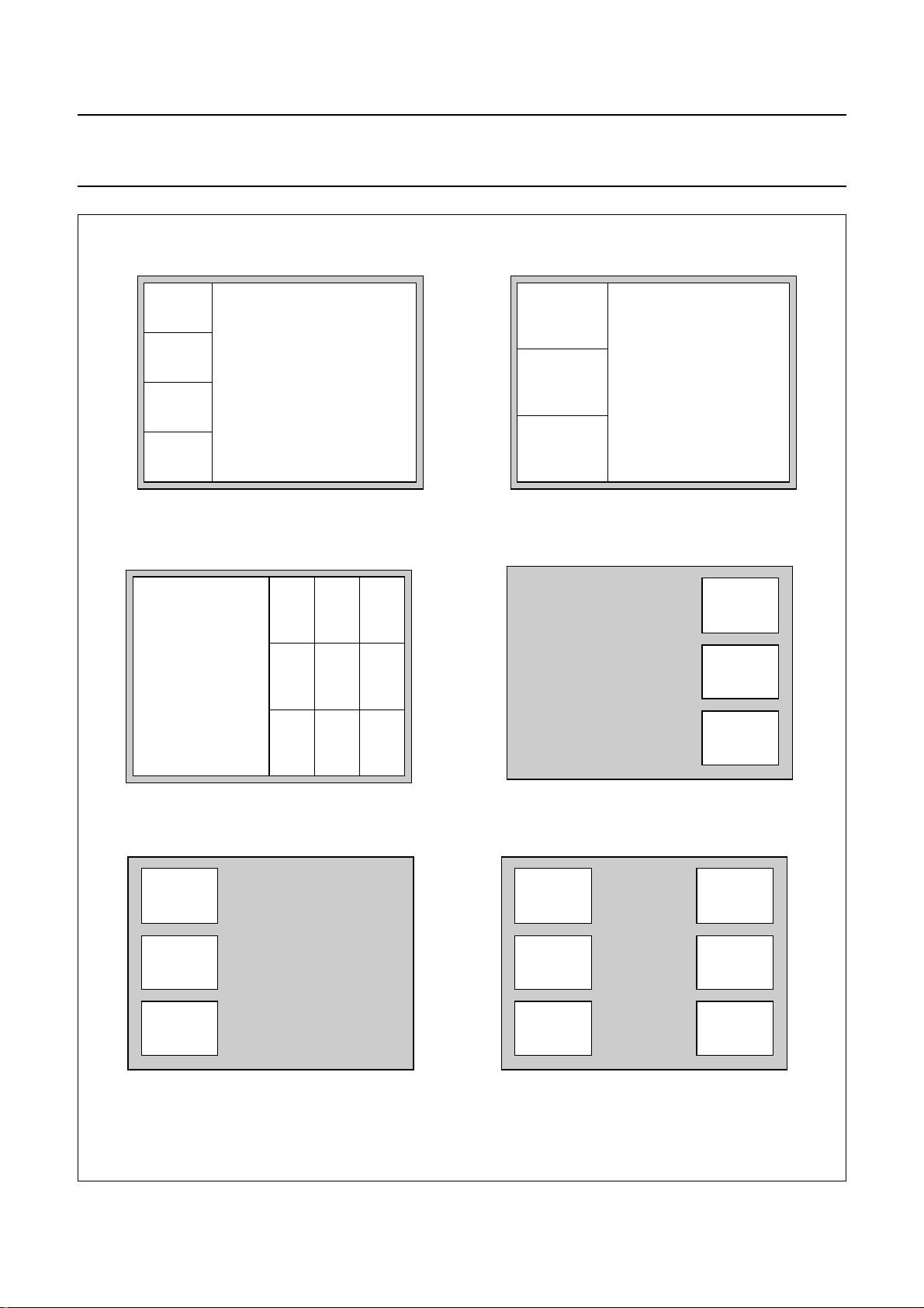
PIP modes
An overview of the general PIP modes is given in Figs 3, 4 and 5. These pictures do not refer to all possible modes the
device can handle. These modes are guaranteed only when sufficient memory is available and enough time is available
to fetch all data from the memory.
handbook, halfpage
handbook, halfpage
handbook, halfpage
handbook, halfpage
SP-Small
SP-Large
MGD594
MGD596
handbook, halfpage
handbook, halfpage
SP-Medium
DP
MGD595
MGD597
Twin-PIP
MGD598
Fig.3 PIP modes.
2000 Jan 13 10
Full Field Still
Full Field Live
MGD587
Philips Semiconductors Preliminary specification
Multistandard Picture-In-Picture (PIP)
controller
handbook, halfpage
MGS388
handbook, halfpage
SAB9079HS
handbook, halfpage
MGS389
handbook, halfpage
MGS390
handbook, halfpage
POP-Left
MGD588
Fig.4 PIP modes (continued).
2000 Jan 13 11
handbook, halfpage
POP-Right
POP-Double
MGD589
MGD590

Philips Semiconductors Preliminary specification
Multistandard Picture-In-Picture (PIP)
controller
handbook, halfpage
MP7
handbook, halfpage
MGD591
handbook, halfpage
handbook, halfpage
MP8
SAB9079HS
MGD592
Quatro
handbook, halfpage
MP16
MGD584
MGD586
Fig.5 PIP modes (continued).
2000 Jan 13 12
handbook, halfpage
MP9
MP13
MGD585
MGL925

Philips Semiconductors Preliminary specification
Multistandard Picture-In-Picture (PIP)
controller
Acquisition window
The acquisition window is 720 pixels. This is related to a
whole line of 896 pixels. So for PAL will be
acquired from the active video. For NTSC this will be
slightly less .
720
--------- 896
63.5 µs×
The vertical acquisition window is 228 lines for NTSC and
276 lines for PAL. Data will be acquired in a 4 :2:2
format. The acquisition clock is 896 × HSYNC.
Acquisition fine positioning
2
C-bus settings relate to the incoming HSYNC,
All I
whether this is a real HSYNC or a burstkey for horizontal
positioning. The same applys for the incoming VSYNC for
vertical positioning. The relationships between the
acquisition window and the internal clamp pulse are
illustrated in Fig.6. In an application the clamp pulse must
be positioned, by the I2C-bus, between the HSYNC and
the start of the active video of the incoming signal.
720
--------- 896
64 µs×
SAB9079HS
Display window
The display window available for PIP pictures is also
720 pixels wide, related to a 896 pixels line. The vertical
display window is 228 lines for NTSC and 276 lines for
PAL.
Background window
The origin of the display window is referenced to the origin
of the background window. The background area is
768 pixels wide. Vertically it is 238 lines for NTSC and
286 lines for PAL.
Display fine positioning
The I2C-bus defined fine positioning has relationships to
the internal HSYNC and VSYNC as illustrated in Fig.7.
handbook, full pagewidth
The grey area depicts the background.
MAHFP
CIPER
CIDEL
MAVFP
228/276 lines
720 pixels
MGS391
Fig.6 Acquisition fine positioning.
2000 Jan 13 13

Philips Semiconductors Preliminary specification
Multistandard Picture-In-Picture (PIP)
controller
handbook, full pagewidth
BGHFP
BGVFP
MDVFP
MDHFP
MAIN CHANNEL
768 pixels
SDHFP
SAB9079HS
SDVFP
SUB CHANNEL
238/286 lines
MGS392
The grey area depicts the background.
Fig.7 Display fine positioning.
YUV to RGB conversion matrix
A YUV to RGB conversion matrix is available. The nine
matrixcoefficientvaluescanbe set by I2C-buscommands.
Two sets can be defined; one for PAL and one for NTSC.
The matrix must be switched on, otherwise a 1 : 1
conversion takes place and Y*, U and V will be
unmodified.
Theconversionmatrix is based on the following equations.
All results (R, G and B) fall in the range from 0 to 1. Any
results outside of this range will be clipped to the nearest
end value. It should be noted that gamma correction is not
applied as is common practice. The end of this section
contains an example.
Normalised Y, U and V (indicated by subscript ‘a’) are
given by the following four equations:
1. Ya=x×Ra+y×Ga+z×B
a
2. x+y+z=1
3. Ua=Ba−Y
4. Va=Ra−Y
a
a
Absolute or discrete (indicated by subscript ‘d’) values
for Y, U and V are given by the following three equations:
1. Yd= 255 × Ya(V), Yanormalised (range 0 to 1)
U
2. ,
3. ,
128 127
U
d
normalised (range −1 to +1)
U
a
128 127
V
d
V
normalised (range −1 to +1)
a
×+=
×+=
a
----------- 1z–
V
a
----------- 1x–
2000 Jan 13 14
Philips Semiconductors Preliminary specification
Multistandard Picture-In-Picture (PIP)
SAB9079HS
controller
Absolute or discrete (indicated by subscript ‘d’) values for R, G and B are given by the following three equations:
RdY
1.
GdY
2.
B
3.
d
The implementation of a matrix with 9 coefficients is shown in Table 1.
Table 1 Matrix coefficients
YUV TO RGB MATRIX
COEFFICIENTS
R ry=1 ru=0
Ggy=1
B by=1 bv=0
255
--------- -
d
127
255
--------- -
d
127
255
Y
--------- -
d
127
V
d
x
-- -
y
U
d
128–()1x–()××+=
128–()1z–()××+=
1x–()× V
d
Y
COFACTOR: Y
255
128–()××–
--------- 127
d
z
1z–()× Ud128–()××–=
-- -
y
U
d
d
COFACTOR:2 × (Ud− 128) COFACTOR: 2 × (Vd− 128)
rv
255
gu
bu
255
--------- 254
--------- 254
z
1z–()××–= gv
-- y
1z–()×=
255
--------- 254
255
--------- 254
V
d
1x–()×=
x
× 1x–()×–=
-- y
So, for example;
R=ry×Y
+ru×2×(Ud− 128) + rv × 2 × (Vd− 128)
d
Table 2 shows how the coefficients can be calculated for a specific case where x = 0.299, y = 0.587 and z = 0.114.
Calculation of xv:y* 128 (rounded to the nearest integer), translates to a binary value. Calculation of xu:xv: translates to
a binary value with the coefficients for the binary bits: −1,1⁄
1
⁄4,1⁄8,1⁄16,1⁄32,1⁄
2
1
⁄
(LSB).
64
128
Table 2 Coefficient calculation
COEFFICIENT EXPRESSION DECIMAL VALUE BINARY VALUE
ry 1 1 10000000
ru 0 0 00000000
rv 0.704 01011010
255
--------- 254
1x–()×
gy 1 1 10000000
gu −0.173 11101010
gv −0.358 11010010
255
--------- 254
255
--------- 254
z
× 1z–()×–
-- y
x
× 1x–()×–
-- y
by 1 1 10000000
bu 0.889 01110010
255
--------- 254
1z–()×
bv 0 0 00000000
2000 Jan 13 15
 Loading...