

Philips SAB9076H-N1, SAB9076H-N2, SAB9076H-N3, SAB9076H-N4 Datasheet
DATA SH EET
Preliminary specification
File under Integrated Circuits, IC02
1996 Aug 13
INTEGRATED CIRCUITS
SAB9076H
Picture-In-Picture (PIP) controller

1996 Aug 13 2
Philips Semiconductors Preliminary specification
Picture-In-Picture (PIP) controller SAB9076H
FEATURES
Display
• Twin PIP in interlaced mode at 8-bit resolution
• Sub-title mode features built in
• Large display fine positioning area, both channels
independent
• Only 2 Mbit required as external VDRAM
(2 × 1 Mbit or 1 × 2 Mbit)
• Four 8-bit Analogue Digital Converters (ADCs; > 7-bit
performance) with clamp circuit
• Most PIP modes handle interlaced pictures without joint
line error
• Two PLLs which generate the line-locked clocks for the
acquisition channels
• Display PLL to generate line-locked clock for the display
• Three 8-bit Digital Analogue Converters (DACs)
• 4:1:1 data format
• Data reduction factors 1 to 1, 1 to 2, 1 to 3 and 1 to 4,
horizontal and vertical independent.
I
2
C-bus programmable
• Single and double PIP modes can be set
• Full field still mode available
• Several aspect ratios can be handled
• Reduction factors can be set freely
• Selection of vertical filtering type
• Freeze of live pictures
• Fine tuned display position, H (8-bit), V (8-bit),
both channels independent
• Fine tuned acquisition area, H (4-bit), V (8-bit),
both channels independent
• Eight main borders, sub-borders and background
colours selectable
• Border and background brightness adjustable, 30%,
50%, 70% and 100% IRE
• Several type of decoder input signals can be set.
GENERAL DESCRIPTION
The SAB9076H is a picture-in-picture controller for NTSC
TV-sets. The circuit contains ADCs, reduction circuitry,
memory control, display control and DACs.
The device inserts one or two live video signals with
original or reduced sizes into a live video signal. All video
signals are expected to be analog baseband signals.
The conversion into the digital environment and back to
the analog environment is carried out on chip. Internal
clocks are generated by two acquisition PLLs and a
display PLL.
Due to the two PIP channels and a large external memory
a wide range of PIP modes are offered. The emphasis is
put on single-PIP, double-PIP, split-screen mode and a
many multi-PIP modes.
1996 Aug 13 3
Philips Semiconductors Preliminary specification
Picture-In-Picture (PIP) controller SAB9076H
QUICK REFERENCE DATA
Note
1. The internal system frequency is 1728 times the H
Sync
input frequency for both the Acquisition and Display PLLs.
ORDERING INFORMATION
Note
1. When using IR reflow soldering it is recommended that the Drypack instructions in the
“Quality Reference Handbook”
(order number 9398 510 63011) are followed.
SYMBOL PARAMETER CONDITIONS MIN. TYP. MAX. UNIT
V
DD
supply voltage 4.5 5.0 5.5 V
I
DD
supply current − 200 − mA
f
sys
system frequency note 1 − 27 − MHz
f
loop
PLL loop bandwidth frequency 4 −−kHz
t
jitter
PLL short term stability time jitter during 1 line (64 µs) −−4ns
ς PLL damping factor − 0.7 −−
TYPE
NUMBER
PACKAGE
NAME DESCRIPTION VERSION
SAB9076H QFP100
(1)
plastic quad flat package; 100 leads (lead length 1.95 mm);
body 14 × 20 × 2.8 mm
SOT317-2
1996 Aug 13 4
Philips Semiconductors Preliminary specification
Picture-In-Picture (PIP) controller SAB9076H
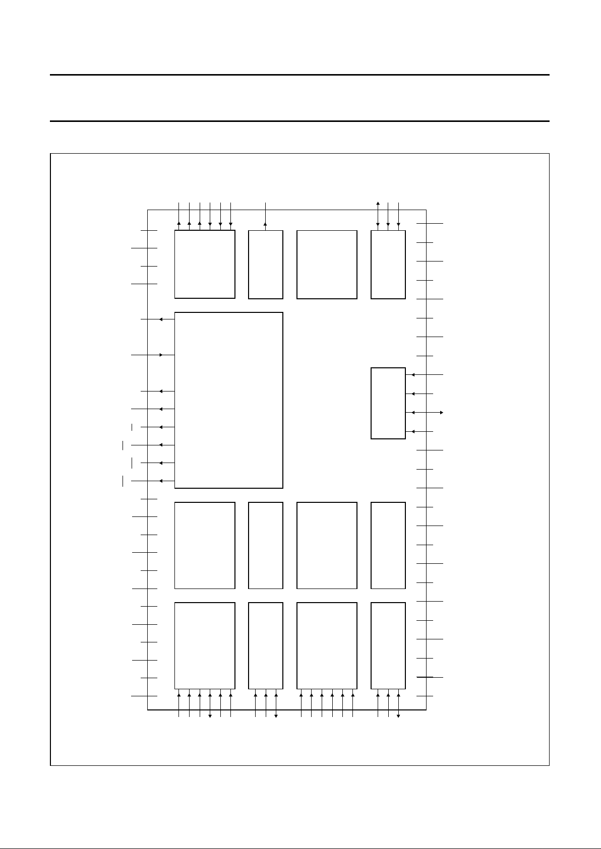
BLOCK DIAGRAM
andbook, full pagewidth
MGC962
SYSUSV
SAV
bias
MAV
DDD
MAV
SSD
MAV
DDA
MAV
SSA
SAV
refT
SAV
refB
71
3
4 12 11
DAV
DDD
DAV
SSD
DAV
DDA
DAV
SSA
TACLKTC
TDCLKTM2
TM1
TM0
A0
SCL
SDA
POR
MCV
DDD
MCV
SSD
DCV
SSD
DCV
DDD
DV
DDD
DV
SSD
V
SSD
V
DDD
SCV
SSD
SCV
DDD
SPV
DDA
SPV
SSA
DPV
SSA
DPV
DDA
MPV
DDA
MPV
SSA
91
92 84 83
100
6318192221201516596061628281 4142434445466566979899
SAV
DDD
SAV
SSD
SAV
DDA
SAV
SSA
78
77 69 70
SV
DDD
SV
SSD
MV
DDD
MV
SSD
68
67 13 14
CAS
RAS
49 48
DAO0 to DAO7
47
31 40 32, 34, 36,
38, 39, 37,
35, 33
DAI0 to DAI7
23, 25, 27,
29, 30, 28,
26, 24
AD0 to AD8
51, 53, 55,
57, 58, 56,
54, 52, 50
75
73
767472
DYDUDV
DAV
bias
DAV
refT
DAV
refB
869088
858789
DFB
93
DT
WE SC
DAC
AND
BUFFER
CLAMP AND ADC
MYMUMV
MAV
bias
MAV
refT
MAV
refB
1068
579
CLAMP AND ADC
SPH
syncSVsync
SPV
bias
796480
PLL AND CLOCK
GENERATOR
HORIZONTAL
AND
VERTICAL
FILTER
HORIZONTAL
AND
VERTICAL
FILTER
MPH
syncMVsync
MPV
bias
2171
PLL AND CLOCK
GENERATOR
DPH
sync
DV
sync
DPV
bias
969495
PLL AND CLOCK
GENERATOR
LINE MEMORY
VDRAM CONTROL AND (RE-) FORMATTING
DISPLAY
CONTROL
LINE MEMORY
I
2
C-BUS CONTROL
LINE MEMORYSAB9076H
Fig.1 Block diagram.
1996 Aug 13 5
Philips Semiconductors Preliminary specification
Picture-In-Picture (PIP) controller SAB9076H
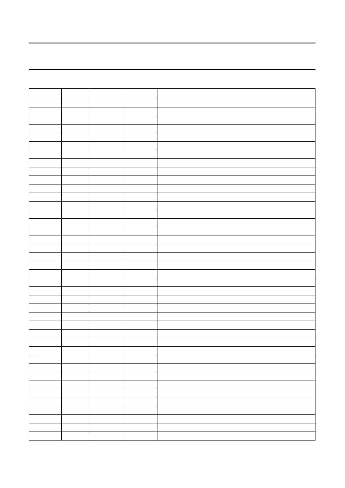
PINNING
SYMBOL PIN I/O TYPE DESCRIPTION
MPV
bias
1 I/O E027 analog bias reference for main channel
MPH
sync
2 I HPP01 horizontal synchronization input for main channel
MAV
SSD
3 I/O E009 digital ground for main channel ADCs and PLLs
MAV
DDD
4 I/O E030 digital positive power supply for main channel ADCs and PLLs
MAV
bias
5 I E027 analog bias reference input for main channel ADCs
MU 6 I E027 analog U input for main channel
MAV
refT
7 I E027 analog top reference voltage input for main channel ADCs
MV 8 I E027 analog V input for main channel
MAV
refB
9 I E027 analog bottom reference voltage input for main channel ADCs
MY 10 I E027 analog Y input for main channel
MAV
DDA
11 I/O E030 analog positive power supply for main channel ADCs
MAV
SSA
12 I/O E009 analog ground for main channel ADCs
MV
SSD
13 I/O E009 digital ground for main-channel core
MV
DDD
14 I/O E030 digital positive power supply for main-channel core
MCV
DDD
15 I/O E030 digital positive power supply for main-clock buffer
MCV
SSD
16 I/O E009 digital ground for main-clock buffer
MV
sync
17 I HPP01 vertical synchronization input for main channel
TDCLK 18 I HPP01 test clock input for display
TC 19 I HPP01 test control input
TM0 20 I HPP01 test mode 0 input
TM1 21 I HPP01 test mode 1 input
n.c. 22 −−not connected
DAI0 23 I HPP01 data bus input from memory; bit 0
DAI7 24 I HPP01 data bus input from memory; bit 7
DAI1 25 I HPP01 data bus input from memory; bit 1
DAI6 26 I HPP01 data bus input from memory; bit 6
DAI2 27 I HPP01 data bus input from memory; bit 2
DAI5 28 I HPP01 data bus input from memory; bit 5
DAI3 29 I HPP01 data bus input from memory; bit 3
DAI4 30 I HPP01 data bus input from memory; bit 4
DT 31 O OPF20 memory data transfer output; active LOW
DAO0 32 O OPF20 data bus output to memory; bit 0
DAO7 33 O OPF20 data bus output to memory; bit 7
DAO1 34 O OPF20 data bus output to memory; bit 1
DAO6 35 O OPF20 data bus output to memory; bit 6
DAO2 36 O OPF20 data bus output to memory; bit 2
DAO5 37 O OPF20 data bus output to memory; bit 5
DAO3 38 O OPF20 data bus output to memory; bit 3
DAO4 39 O OPF20 data bus output to memory; bit 4
SC 40 O OPF20 memory shift clock output
1996 Aug 13 6
Philips Semiconductors Preliminary specification
Picture-In-Picture (PIP) controller SAB9076H
DCV
SSD
41 I/O E009 digital ground for display-clock buffer
DCV
DDD
42 I/O E030 digital positive power supply for display-clock buffer
DV
DDD
43 I/O E030 digital positive power supply for display core
DV
SSD
44 I/O E009 digital ground for display core
V
SSD
45 I/O E009 digital ground for peripherals
V
DDD
46 I/O E030 digital positive power supply for peripherals
WE 47 O OPF20 memory write enable output; active LOW
CAS 48 O OPF20 memory column address strobe output; active LOW
RAS 49 O OPF20 memory row address strobe output; active LOW
AD8 50 O OPF20 memory address bus output; bit 8
AD0 51 O OPF20 memory address bus output; bit 0
AD7 52 O OPF20 memory address bus output; bit 7
AD1 53 O OPF20 memory address bus output; bit 1
AD6 54 O OPF20 memory address bus output; bit 6
AD2 55 O OPF20 memory address bus output; bit 2
AD5 56 O OPF20 memory address bus output; bit 5
AD3 57 O OPF20 memory address bus output; bit 3
AD4 58 O OPF20 memory address bus output; bit 4
A0 59 I HPF01 I
2
C-bus address 0 selection input
SCL 60 I HPF01 shift clock input for I
2
C-bus
SDA 61 I/O IOI41 shift I
2
C-bus input data; acknowledge I2C-bus output data
POR 62 I HUP07 power-on reset input
TACLK 63 I HPP01 test clock input for acquisition
SV
sync
64 I HPP01 vertical synchronization input for sub-channel
SCV
SSD
65 I/O E009 digital ground for sub-clock buffer
SCV
DDD
66 I/O E030 digital positive power supply for sub-clock buffer
SV
DDD
67 I/O E030 digital positive power supply for sub-channel core
SV
SSD
68 I/O E009 digital ground for sub-channel core
SAV
SSA
69 I/O E009 analog ground for sub-channel ADCs
SAV
DDA
70 I/O E030 analog positive power supply for sub-channel ADCs
SY 71 I E027 analog Y input for sub-channel
SAV
refB
72 I E027 analog bottom reference input voltage for sub-channel ADCs
SV 73 I E027 analog V input for sub-channel
SAV
refT
74 I E027 analog top reference input voltage for sub-channel ADCs
SU 75 I E027 analog U input for sub-channel
SAV
bias
76 I/O E027 analog bias reference input/output for sub-channel ADCs
SAV
DDD
77 I/O E030 digital positive power supply for sub-channel ADCs and PLLs
SAV
SSD
78 I/O E009 digital ground for sub-channel ADCs and PLLs
SPH
sync
79 I HPP01 horizontal synchronization input for sub-channel
SPV
bias
80 I/O E027 analog bias reference input/output for sub-channel
SPV
SSA
81 I/O E009 analog ground for sub-channel PLL
SYMBOL PIN I/O TYPE DESCRIPTION
1996 Aug 13 7
Philips Semiconductors Preliminary specification
Picture-In-Picture (PIP) controller SAB9076H
Table 1 Pin type explanation
SPV
DDA
82 I/O E030 analog positive power supply for sub-channel PLL
DAV
DDA
83 I/O E030 analog positive power supply for DACs
DAV
SSA
84 I/O E009 analog ground for DACs
DAV
bias
85 I E027 analog bias voltage reference input for DACs
DY 86 O E027 analog Y output of DAC
DAV
refT
87 I E027 analog top reference input voltage for DACs
DV 88 O E027 analog V output of DAC
DAV
refB
89 I E027 analog bottom reference input voltage for DACs
DU 90 O E027 analog U output of DAC
DAV
SSD
91 I/O E009 digital ground for DACs
DAV
DDD
92 I/O E030 digital positive power supply for DACs
DFB 93 O OPF20 fast blanking control output signal
DV
sync
94 I HPP01 vertical synchronization input for display channel
DPH
sync
95 I HPP01 horizontal synchronization input for display PLL
DPV
bias
96 I/O E027 analog bias voltage reference input/output for display PLL
DPV
SSA
97 I/O E009 analog ground for display PLL
DPV
DDA
98 I/O E030 analog positive power supply for display PLL
MPV
DDA
99 I/O E030 analog positive power supply for main channel PLL
MPV
SSA
100 I/O E009 analog ground for main channel PLL
PIN TYPE DESCRIPTION
E030 V
DD
pin; diode to V
SS
E009 VSSpin; diode to V
DD
E027 analog input pin; diode to VDD and V
SS
HPF01 digital input pin; CMOS levels, diode to V
SS
HPP01 digital input pin; CMOS levels, diode to VDD and V
SS
HUP07 digital input pin; CMOS levels with hysteresis, pull-up resistor to VDD, diode to VDD and V
SS
IOI41 I2C-bus pull-down output stage; CMOS input levels, diode to V
SS
OPF20 digital output pin; CMOS levels
SYMBOL PIN I/O TYPE DESCRIPTION
1996 Aug 13 8
Philips Semiconductors Preliminary specification
Picture-In-Picture (PIP) controller SAB9076H
handbook, full pagewidth
80
79
78
77
76
75
74
73
72
71
70
69
68
67
66
65
64
63
62
61
60
59
58
57
56
55
54
53
52
5130
29
28
27
26
25
24
23
22
21
20
19
18
17
16
15
14
13
12
11
10
9
8
7
6
5
4
3
2
1
100
99989796959493929190898887868584838281
31323334353637383940414243444546474849
50
MGC963
SAB9076H
MPV
bias
MPH
sync
MAV
SSD
MAV
DDD
MAV
bias
MU
MAV
refT
MV
MAV
refB
MY
MAV
DDA
MAV
SSA
MV
SSD
MV
DDD
MCV
DDD
MCV
SSD
MV
sync
TDCLK
TC
TM0
TM1
n.c.
DAI0
DAI7
DAI1
DAI6
DAI2
DAI5
DAI3
DAI4
DT
DAO0
DAO7
DAO1
DAO6
DAO2
DAO5
DAO3
DAO4
SC
DCV
SSD
DCV
DDD
DV
DDD
DV
SSDVSSD
V
DDD
WE
CAS
RAS
AD8
SPV
bias
SPH
sync
SAV
SSD
SAV
DDD
SAV
bias
SU
SAV
refT
SV
SAV
refB
SY
SAV
DDA
SAV
SSA
SV
SSD
SV
DDD
SCV
DDD
SCV
SSD
SV
sync
TACLK
POR
SDA
SCL
A0
AD4
AD3
AD5
AD2
AD6
AD1
AD7
AD0
MPV
SSA
MPV
DDA
DPV
DDA
DPV
SSA
DPV
bias
DPH
sync
DV
sync
DFB
DAV
DDD
DAV
SSD
DU
DAV
refB
DV
DAV
refT
DY
DAV
bias
DAV
SSA
DAV
DDA
SPV
DDA
SPV
SSA
Fig.2 Pin configuration.
1996 Aug 13 9
Philips Semiconductors Preliminary specification
Picture-In-Picture (PIP) controller SAB9076H
FUNCTIONAL DESCRIPTION
Pixel rate
The internal chrominance format used is 4 : 1 : 1. It is
expected that the bandwidth of the input signals is limited
to 4.5 MHz for the Y input and 1.125 MHz for the U/V input.
The Y input is sampled with a 1728 × HS (≈27.0 MHz)
clock and is filtered and down sampled to the internal
864 × HS (≈13.5 MHz) pixel rate.
The U and V inputs are multiplexed and sampled with a
432 × HS clock and down sampled to the internal
216 × HS (≈3.375 MHz) pixel rate.
Acquisition area
Synchronisation is achieved via the acquisition H
Sync
and
V
sync
pins. With the acquisition fine positioning added to a
system constant the starting point of the acquisition can be
controlled.
The acquisition area is 672 pixels/line and 228 lines/field
for NTSC. Both main and sub-channels are equivalent in
handling the data.
Display mode
The internal display pixel rate is 864 × DPH
sync
which is
13.5 MHz. This pixel rate is up sampled by interpolation to
1728 × DPH
sync
before the DAC stage.
Display area
The display background is an area of 696 pixels and
238 lines. This can be put on/off by the BGON bit
independent of the PIPON bit. This area can be moved by
the display background fine positioning (BGHFP and
BGVFP registers). Its colour is determined by the BGCOL
and BGBRT registers.
Within this area PIPs are defined dependent on the PIP
mode. The PIP sizes are determined by the display
reduction factors as is shown in Table 2.
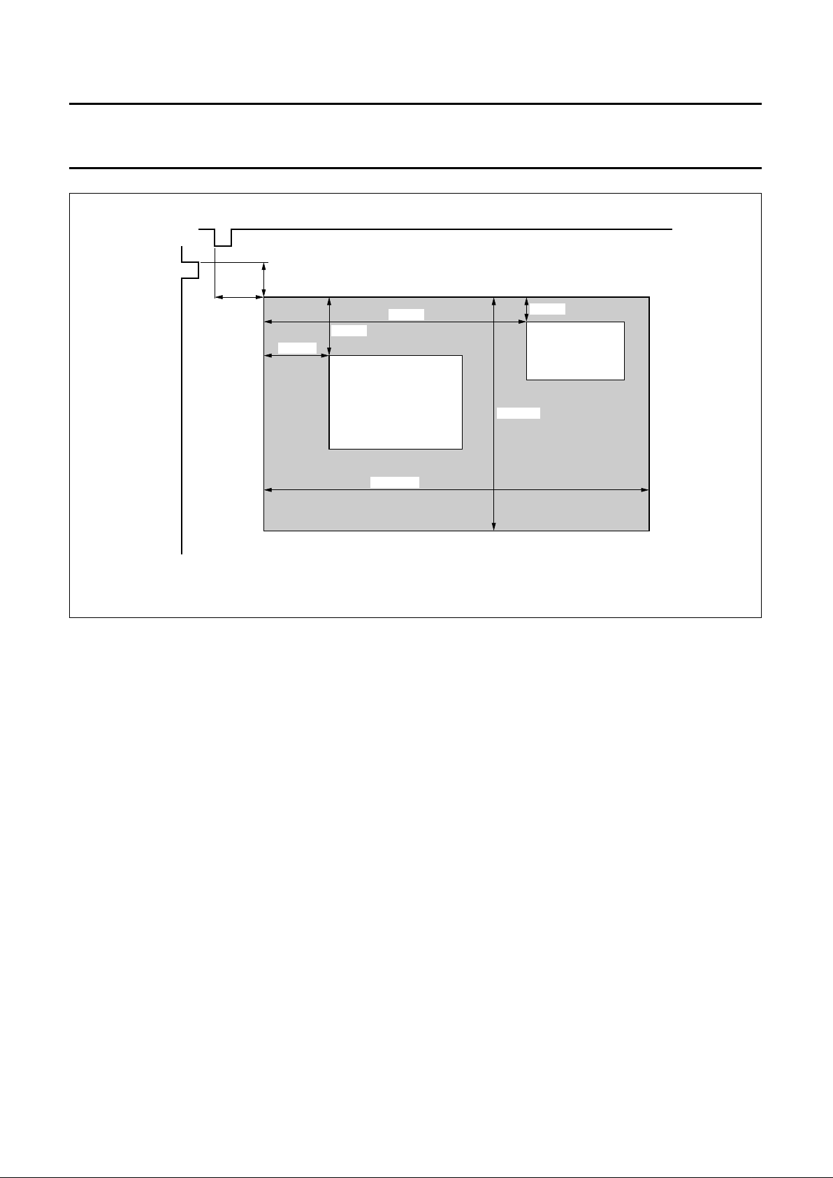
The display fine positioning determines the location of the
PIPs with respect to the background. Sub-channel and
main channel both have their independent PIP size and
location control, which is shown in Fig.3.
Table 2 PIP sizes
REDUCTION H/1 H/2 H/3 H/4 V/1 V/2 V/3 V/4
Pixels 672 336 224 168 −−−−
Lines −−−−228 114 76 57
1996 Aug 13 10
Philips Semiconductors Preliminary specification
Picture-In-Picture (PIP) controller SAB9076H
Fig.3 Display fine positioning.
handbook, full pagewidth
MGC964
BGHFP
BGVFP
MAIN CHANNEL
SUB CHANNEL
SAHFP
MAVFP
238 lines
MAHFP
SAVFP
696 pixels
PIP modes
The two independent acquisition channels can be
controlled independently on the display side. A wide
variety of modes is possible but a subset of 7 modes is
fixed and can be set easily by the I2C-bus. An overview of
the preconditioned modes is given in Table 3. For all PIP
modes the main and sub-display fine positioning must be
set to obtain a display configuration.
D
ATA TRANSFER
The internal data path has an 8-bit resolution and 4 :1:1
data format. The communication to the external VDRAM
takes place at 864 × H
sync
(both display and acquisition).
Approximately 800 8-bit words can be fetched from the
external VDRAM in one display line which is not enough to
display one complete display line with true 8-bit resolution.
Two methods of reducing data are available. One is simply
skipping the 8-bit to 6-bit (SKIP6, I
2
C-bus bit) and the other
is a small form of data reduction to come from 8-bit to 6-bit
(SMART6, I2C-bus bit). If both bits are set to logic 0 the
device is in true 8-bit resolution mode. For the twin PIP
mode the main channel is not placed in the VDRAM but in
an internal buffer, so still 8-bit resolution is achieved.
 Loading...