Philips sab9075h DATASHEETS

INTEGRATED CIRCUITS
DATA SH EET
SAB9075H
Picture-in-Picture (PIP) controller
for NTSC
Preliminary specification
File under Integrated Circuits, IC02
Philips Semiconductors
February 1995

Philips Semiconductors Preliminary specification
Picture-in-Picture (PIP) controller for NTSC SAB9075H
FEATURES
Display
• One or two live pictures can be displayed
simultaneously
• Wide range of multi-Picture-In-Picture (PIP) modes
available
• Six 6-bit Analog-to-Digital Converters (ADC) with
clamping circuit
• Enhanced vertical resolution at most modes for live
pictures
• Two Phase-Locked-Loops (PLL) with Voltage
Controlled Oscillator (VCO) to generate the line-locked
clocks
• Three 7-bit Digital-to-Analog Converters (DAC)
• 4:1:1 data format
• Data reduction factors 1 to 4, 1 to 9 and 1 to 16.
2
I
C-bus programmable
• Different single, double and multi-PIP modes can be set
• Several aspect ratios can be handled
• Reduction factors can be set automatically and
manually
• Selection of vertical filtering type
• Freeze of live pictures
• Single-PIP display position, four corners on-screen
• Multi-PIP display position, left or right on-screen
• Fine tuned display position, H (6-bit), V (6-bit)
• Fine tuned acquisition area, H (4-bit), V (4-bit)
• Channel-border and live PIP selectable
• Eight main-border, sub-border, channel-border and
background colours selectable
• Border and background brightness adjustable, 30%,
50%, 70% and 100% IRE
• Several types of decoder input signals can be set
• 6-bit HUE and SAT signals (0 to 5 V) adjustable by
I2C-bus
• Main and sub-audio mute controllable by I2C-bus.
GENERAL DESCRIPTION
The SAB9075H is a picture-in-picture controller for the
NTSC environment in combination with the Integrated
NTSC decoder and sync processor TDA8315.
The device inserts one or two live video channels with
reduced sizes into a live video signal. All video signals are
expected to be analog baseband signals. The conversion
into the digital environment and back to the analog
environment is carried out on-chip. Internal clocks are
generated by two PLLs.
Due to the two PIP channels and a large external memory,
a wide range of PIP modes are offered. The emphasis is
put on double-PIP and multi-PIP modes. In combination
with the different border colours and some external
software the IC concept can be used as an excellent
channel selection tool.
2
Some of the I
saturation and HUE of the colours. There are also outputs
for the mute function of main and sub-channel.
C-bus registers are for controlling the
February 1995 2
Philips Semiconductors Preliminary specification
Picture-in-Picture (PIP) controller for NTSC SAB9075H
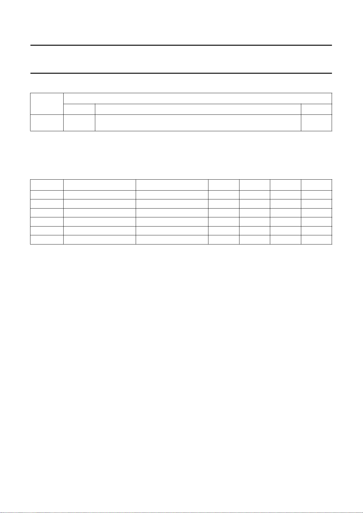
ORDERING INFORMATION
TYPE
NUMBER
NAME DESCRIPTION VERSION
SAB9075H QFP100
(1)
plastic quad flat package; 100 leads (lead length 1.95 mm);
PACKAGE
SOT317-2
body 14 × 20 × 2.8 mm
Note
1. When using IR reflow soldering it is recommended that the Drypack instructions in the
“Quality Reference Handbook”
(order number 9398 510 63011) are followed.
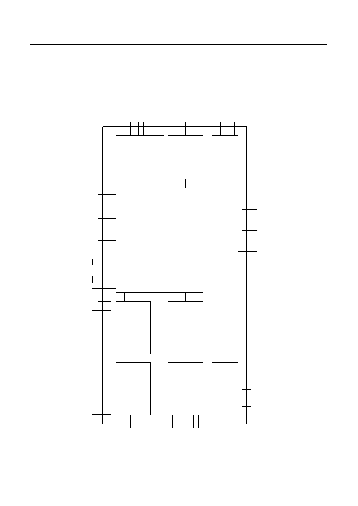
QUICK REFERENCE DATA
SYMBOL PARAMETER CONDITIONS MIN. TYP. MAX. UNIT
V
I
tot
f
sys
f
loop
t
jitter
DD
supply voltage all positive supply pins 4.5 5.0 5.5 V
total supply current note 1 tbf 220 tbf mA
system frequency note 2 − 27 30 MHz
loop bandwidth frequency 4 −−kHz
short term stability time jitter during 1 line (64 µs) −−4ns
ς damping factor − 0.7 −−
Notes
1. Digital clocks are silent and analog bias current is zero.
2. The internal system frequencies are 1728 times the input frequency. For more detailed information about the clock
generation see Section “PLLs and clock generation”.
February 1995 3
Philips Semiconductors Preliminary specification
Picture-in-Picture (PIP) controller for NTSC SAB9075H
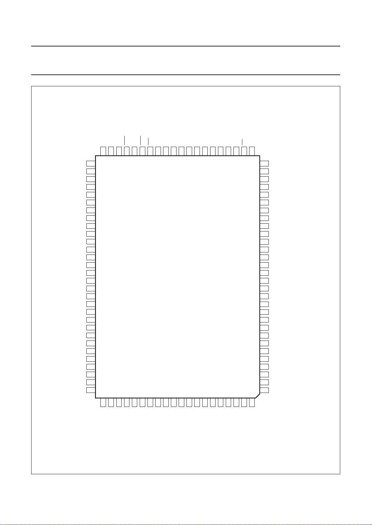
BLOCK DIAGRAM
refTU
refTV
refTY
bias
DAI
DAV
DAV
DAV
DBF
SCL66SDA63POR64A0
book, full pagewidth
SSA
SSD
DAV DAV
SC
WE
RAS
SSD
MV
SSD
SV
SSA
SAV
SSD
SAV
SSA
MAV
SSD
MAV
DDA
DDD
DAV DAV
AD0 to 8
DAI0 to 7
DAO0 to 7
DT
CAS
DDD
MV
DDD
SV
DDA
SAV
DDD
SAV
DDA
MAV
DDD
MAV
18DY14DU16DV19
11 10 20 21
48 to 56
26,25,30,28
41,46,37,34
27 29,31,35,33
47 45 44 32 36,39,40,38
72 73 9 8
82 81 89 90
99 100 92 91
98
MAIN
ACQUISITION
CLAMP AND
A/D CONVERTER
94MY96MV93
13
15
17
AND BUFFER
D/A CONVERTER
MEMORY
CONTROL
SAB9075H
97
95
87
83SY85SV88
24
DISPLAY
SUB
ACQUISITION
CLAMP AND
A/D CONVERTER
86
84
65
7565861
2
I C-BUS
6059
21
3457
79
AND PLL BLOCK
DISPLAY TIMING CONTROL
HUE AND SAT
70
69
67
78
77
76 80
71 23 74
22 42 43
D/A CONVERTERS
68
MBE084
MTCLK
TM2
TM0
SSA
MPV
SSD
MPV
sync
MH
SSA
SPV
bias
SPI
DDD
SPV
sync
SV
SSS
V
DDD
V
VDD
2
I C
STCLK
TC
TM1
DDA
MPV
DDD
MPV
bias
MPI
DDA
SPV
sync
SH
SSD
SPV
sync
MV
Fig.1 Block diagram.
February 1995 4
MU
bias
MAI
refT
MAV
refB
MAV
SU
bias
SAI
refT
SAV
refB
SAV
HUE
SAT
SMUTE
MMUTE

Philips Semiconductors Preliminary specification
Picture-in-Picture (PIP) controller for NTSC SAB9075H
PINNING
SYMBOL PIN I/O TYPE DESCRIPTION
MPV
DDA
MPV
SSA
MH
sync
MPI
bias
MPV
SSD
MTCLK 6 I HPP01 test clock for main-channel
MPV
DDD
MV
DDD
MV
SSD
DAV
DDD
DAV
SSD
n.c. 12 −−not connected
DAV
refTU
DU 14 O E027 analog U output
DAV
refTV
DV 16 O E027 analog V output
DAV
refTY
DY 18 O E027 analog Y output
DAI
bias
DAV
SSA
DAV
DDA
2
CV
I
DD
MV
sync
DBF 24 O SPF20 fast blanking control output signal
DAI5 25 I HPP01 data bus input from memory; bit 5
DAI4 26 I HPP01 data bus input from memory; bit 4
SC 27 O OPF20 memory shift clock
DAI7 28 I HPP01 data bus input from memory; bit 7
DAI0 29 I HPP01 data bus input from memory; bit 0
DAI6 30 I HPP01 data bus input from memory; bit 6
DAI1 31 I HPP01 data bus input from memory; bit 1
DT 32 O OPF20 memory data transfer; active LOW
DAI3 33 I HPP01 data bus input from memory; bit 3
DAO7 34 O OPF20 data bus output to memory; bit 7
DAI2 35 I HPP01 data bus input from memory; bit 2
DAO0 36 O OPF20 data bus output to memory; bit 0
DAO6 37 O OPF20 data bus output to memory; bit 6
DAO3 38 O OPF20 data bus output to memory; bit 3
DAO1 39 O OPF20 data bus output to memory; bit 1
DAO2 40 O OPF20 data bus output to memory; bit 2
1 I/O E030 analog positive power supply for PLL main-channel
2 I/O E009 analog negative power supply for PLL main-channel
3 I E027 horizontal synchronization for main-channel
4 I E027 analog bias reference current for PLL main-channel
5 I/O E009 digital negative power supply for PLL main-channel
7 I/O E030 digital positive power supply for PLL main-channel
8 I/O E030 digital positive power supply for main-channel core
9 I/O E009 digital negative power supply for main-channel core
10 I/O E030 digital positive power supply for DACs
11 I/O E009 digital negative power supply for DACs
13 I/O E027 analog reference voltage for top U DAC
15 I/O E027 analog reference voltage for top V DAC
17 I/O E027 analog reference voltage for top Y DAC
19 I E027 analog bias reference current for DACs
20 I/O E009 analog negative power supply for DACs
21 I/O E030 analog positive power supply for DACs
22 I/O E030 positive supply for HUE and SAT decoders
23 I HPP01 vertical synchronization for main-channel
February 1995 5

Philips Semiconductors Preliminary specification
Picture-in-Picture (PIP) controller for NTSC SAB9075H
SYMBOL PIN I/O TYPE DESCRIPTION
DAO4 41 O OPF20 data bus output to memory; bit 4
V
DDD
V
SSS
WE 44 O OPF20 memory write enable; active LOW
CAS 45 O OPF20 memory column address strobe; active LOW
DAO5 46 O OPF20 data bus output to memory; bit 5
RAS 47 O OPF20 memory row address strobe; active LOW
AD0 48 O OPF20 memory address bus; bit 0
AD8 49 O OPF20 memory address bus; bit 8
AD1 50 O OPF20 memory address bus; bit 1
AD6 51 O OPF20 memory address bus; bit 6
AD2 52 O OPF20 memory address bus; bit 2
AD5 53 O OPF20 memory address bus; bit 5
AD3 54 O OPF20 memory address bus; bit 3
AD4 55 O OPF20 memory address bus; bit 4
AD7 56 O OPF20 memory address bus; bit 7
n.c. 57 −−not connected
TC 58 I HPP01 test control
TM0 59 I HPP01 test mode 0
TM1 60 I HPP01 test mode 1
TM2 61 I HPP01 test mode 2
n.c. 62 −−not connected
POR 63 I HUP07 power-on reset
A0 64 I HPF01 I
SCL 65 I HPF01 shift clock for I
SDA 66 I/O IOI41 shift I
MMUTE 67 O SPF20 mute output for main-channel
SMUTE 68 O SPF20 mute output for sub-channel
SAT 69 O E027 analog output for SAT decoder
HUE 70 O E027 analog output for HUE decoder
SV
sync
SV
SSD
SV
DDD
SPV
DDD
STCLK 75 I HPP01 test clock for sub-channel
SPV
SSD
SPI
bias
SH
sync
SPV
SSA
SPV
DDA
SAV
DDD
42 I/O E030 digital positive power supply for peripherals
43 I/O E009 digital negative power supply for peripherals
2
C-bus address 0 selection pin
2
C-bus
2
C-bus input data; acknowledge I2C-bus output data
71 I HPP01 vertical synchronization for sub-channel
72 I/O E009 digital negative power supply for sub-channel core
73 I/O E030 digital positive power supply for sub-channel core
74 I/O E030 digital positive power supply for PLL sub-channel
76 I/O E009 digital negative power supply for PLL sub-channel
77 I E027 analog bias reference current for PLL sub-channel
78 I E027 horizontal synchronization for sub-channel
79 I/O E009 analog negative power supply for PLL sub-channel
80 I/O E030 analog positive power supply for PLL sub-channel
81 I/O E030 digital positive power supply for ADC sub-channel
February 1995 6

Philips Semiconductors Preliminary specification
Picture-in-Picture (PIP) controller for NTSC SAB9075H
SYMBOL PIN I/O TYPE DESCRIPTION
SAV
SSD
SU 83 I E027 analog U input for sub-channel
SAV
refB
SV 85 I E027 analog V input for sub-channel
SAV
refT
SY 87 I E027 analog Y input for sub-channel
SAI
bias
SAV
SSA
SAV
DDA
MAV
DDA
MAV
SSA
MAI
bias
MU 94 I E027 analog U input for main-channel
MAV
refB
MV 96 I E027 analog V input for main-channel
MAV
refT
MY 98 I E027 analog Y input for main-channel
MAV
SSD
MAV
DDD
82 I/O E009 digital negative power supply for ADC sub-channel
84 I/O E027 analog reference voltage for bottom ADC sub-channel
86 I/O E027 analog reference voltage for top ADC sub-channel
88 I E027 analog bias reference current for ADC sub-channel
89 I/O E009 analog negative power supply for ADC sub-channel
90 I/O E030 analog positive power supply for ADC sub-channel
91 I/O E030 analog positive power supply for ADC main-channel
92 I/O E009 analog negative power supply for ADC main-channel
93 I E027 analog bias reference current for ADC main-channel
95 I/O E027 analog reference voltage for bottom ADC main-channel
97 I/O E027 analog reference voltage for top ADC main-channel
99 I/O E009 digital negative power supply for ADC main-channel
100 I/O E030 digital positive power supply for ADC main-channel
Table 1 Pin type explanation
PIN TYPE DESCRIPTION
E030 V
E009 VSSpin; diode to V
E027 analog input pin; diode to VDD and V
HPF01 digital input pin; CMOS levels, diode to V
HPP01 digital input pin; CMOS levels, diode to VDD and V
pin; diode to V
DD
SS
DD
SS
SS
SS
HUP07 digital input pin; CMOS levels with hysteresis, pull up resistor to VDD, diode to VDD and V
IOI41 I2C-bus pull-down output stage; CMOS input levels
OPF20 digital output pin
SPF20 digital output pin; slew rate controlled
SS
February 1995 7
Philips Semiconductors Preliminary specification
Picture-in-Picture (PIP) controller for NTSC SAB9075H
SSS
DDD
V
DAO4
DAO2
DAO1
DAO3
DAO6
DAO0
DAI2
DAO7
DAI3DTDAI1
32
33
34
35
36
37
38
39
40
41
42
43
44
SAB9075H
MBE083
31
DAI6
30
DAI0
29
DAI7
28
SC
27
DAI4
26
DAI5
25
DBF
24
sync
23
22
21
20
19
18
17
16
15
14
13
12
11
10
9
8
7
6
5
4
3
2
1
DD
DY
DV
DU
n.c.
DDA
SSA
bias
refTY
refTV
refTU
SSD
DDD
SSD
DDD
DDD
SSD
bias
sync
SSA
DDA
MV
I C V
2
DAV
DAV
DAI
DAV
DAV
DAV
DAV
DAV
MV
MV
MPV
MTCLK
MPV
MPI
MH
MPV
MPV
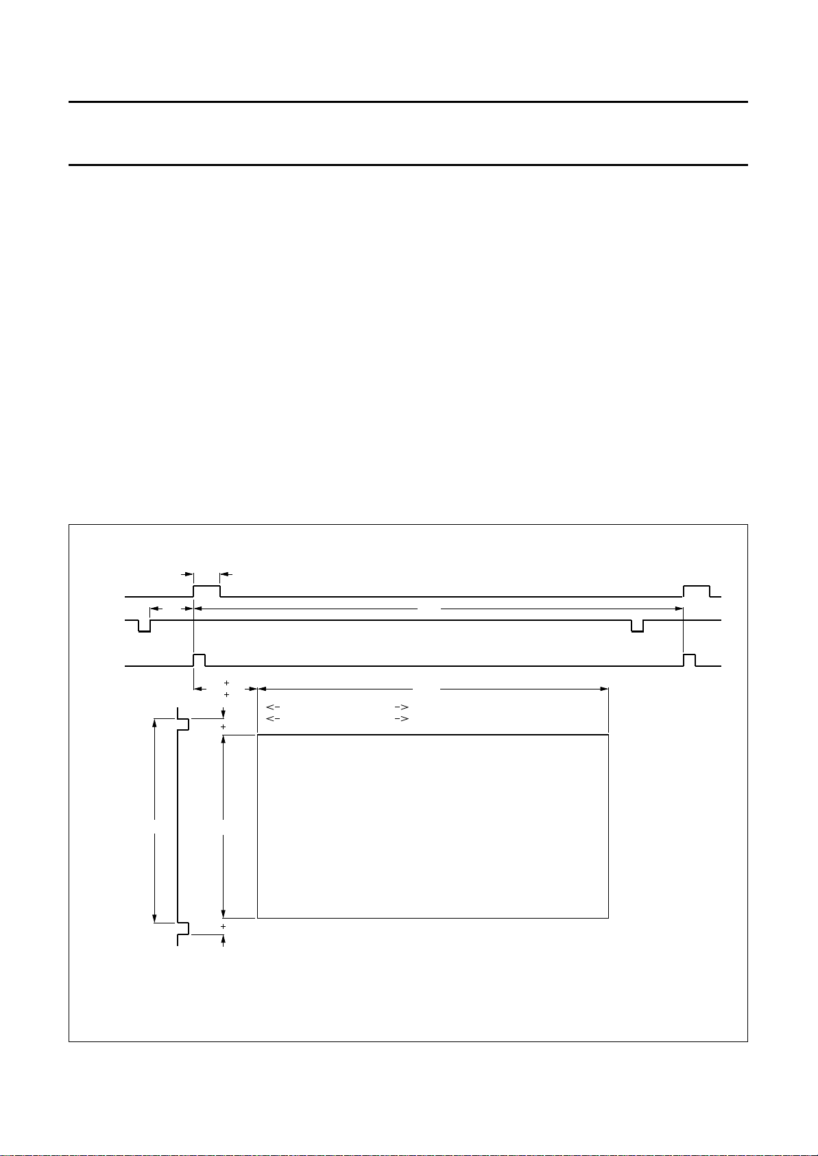
Fig.2 Pin configuration.
sync
SSD
DDD
DDD
SSD
bias
sync
SSA
DDA
AD6
51
AD2
52
53
AD5
54
AD3
AD4
55
AD7
56
57
n.c.
58
TC
TM0
59
TM1
60
61
TM2
62
n.c.
63 POR
64 A0
65
SCL
66 SDA
67 MMUTE
SMUTE
68
69
SAT
70
HUE
71
SV
72
SV
73
SV
74
SPV
75 STCLK
76
SPV
77
SPI
78
SH
79
SPV
80
SPV
50 AD1
AD8
49
AD0
48
RAS
47
DAO5
46
CASWEV
45
February 1995 8
81
DDD
SAV
82
SSD
SAV
83
SU
84
refB
SAV
85
SV
86
refT
SAV
87
SY
88
bias
SAI
89
SSA
SAV
90
DDA
SAV
91
DDA
MAV
92
SSA
MAV
93
bias
MAI
94
MU
95
refB
MAV
96
MV
97
refT
MAV
98
MY
99
SSD
MAV
100
DDD
MAV
Philips Semiconductors Preliminary specification
Picture-in-Picture (PIP) controller for NTSC SAB9075H
FUNCTIONAL DESCRIPTION
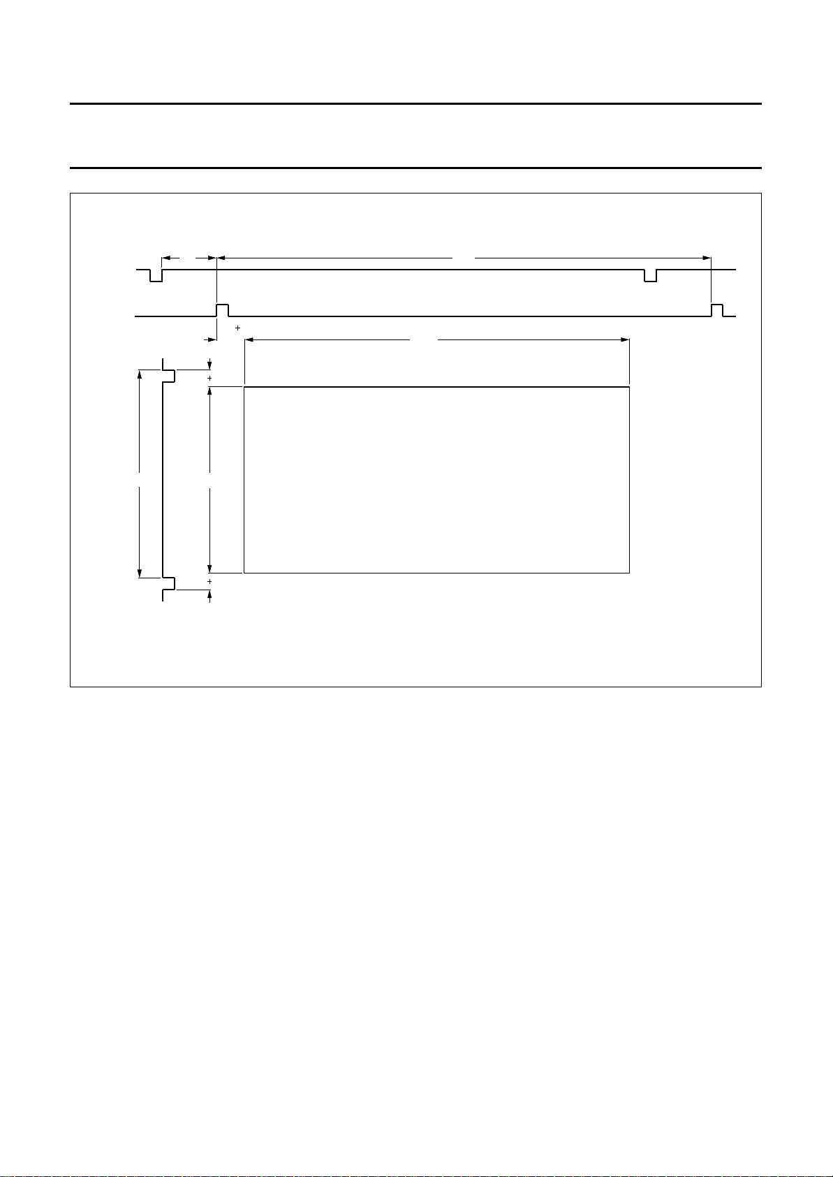
Acquisition area
The acquisition area is in the centre of the visible screen
area. Vertically 228 lines are sampled. Horizontally
672 Y-pixels are processed. The exact active processing
area can be fine tuned in horizontal (2 pixels/steps,
16 steps) and vertical (1 line/step, 16 steps) direction for
both main and sub-channel by the I
2
C-bus (see Fig.3). The
given numbers are pixel numbers at a 13.5 MHz data rate.
The signals, which are dependent on the I2C-bus registers,
can also be related to the H
, in which event they are
sync
delayed by 68 pixels.
Chrominance format
The chrominance format is 4:1:1.
The YUV signals are sampled at a rate of 27 MHz and then
filtered and subsampled to a data rate of 13.5 MHz.
handbook, full pagewidth
clamp
H
sync
32
68
It is expected that the input signals do not contain
frequencies outside the video bandwidth (Y
= 4.5 MHz;
BW
UBWand VBW= 1.125 MHz).
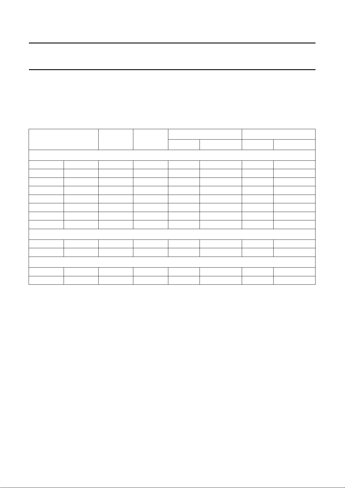
Display area
The display area is shown in Fig.4. The given numbers are
pixels at a data rate of 13.5 MHz. The signals are related
to the burstkey and the V
registers the signals can also be related to the H
. Dependent on the I2C-bus
sync
sync
.
The internal 13.5 MHz data rate is upsampled to the
double frequency (27 MHz) and then fed to the DACs.
2
The display output can be fine positioned by the I
C-bus in
64 steps of 4 pixels in horizontal direction and 64 steps of
1 line/field in vertical direction.
864
burstkey
sync
80 FT
104 FTV
18 FT
228262.5
18 FT
672
624
1/1, 1/3 and 1/4 reduction
1/2 reduction
MBE085
Fig.3 Acquisition area.
February 1995 9
Philips Semiconductors Preliminary specification
Picture-in-Picture (PIP) controller for NTSC SAB9075H
handbook, full pagewidth
H
sync
burstkey
V
sync
68 864
36 FT
672
11 FT
228262.5
11 FT
MBE086
Fig.4 Display area.
February 1995 10
Philips Semiconductors Preliminary specification
Picture-in-Picture (PIP) controller for NTSC SAB9075H
PIP modes
The controller contains two independent acquisition-channels which provide the scaling factors to support the range of
different modes. With the external memory of 2 Mbit it is possible to select between single, double and multi-PIP modes.
Table 2 gives an overview of the different PIP modes.
Table 2 PIP modes
SUB SIZE
(1)
MODE SUB MAIN
PIXELS REDUCTION
4 : 3 main +4:3 subto 4:3screen or 16 : 9 main + 16 : 9 sub to 16 : 9 screen
1
1.1 SPS
1.2 SPL
1.3 DP
⁄
1
⁄
1
⁄
1.4 MP3 3 ×
1.5 MP4 3 ×
1.6 MP7 7 ×
1.7 MP8 7 ×
1.8 MP9 8 ×
16
9
4
1
⁄
16
1
⁄
16
1
⁄
16
1
⁄
16
1
⁄
9
− 160P, 53L1⁄4H,1⁄4V −−
− 216P, 72L1⁄3H,1⁄3V −−
1
⁄
4
304P, 108L1⁄2H,1⁄2V 304P, 108L1⁄2H,1⁄2V
− 160P, 53L1⁄4H,1⁄4V −−
1
⁄
4
160P, 53L1⁄4H,1⁄4V 304P, 108L1⁄2H,1⁄2V
− 160P, 53L1⁄4H,1⁄4V −−
1
⁄
4
1
⁄
9
160P, 53L1⁄4H,1⁄4V 304P, 108L1⁄2H,1⁄2V
216P, 72L1⁄3H,1⁄3V 216P, 72L1⁄3H,1⁄3V
16:9sub+4:3main to 4 : 3 screen
2.1 SPS
2.2 SPL
1
⁄
16
1
⁄
9
− 216P, 53L1⁄3H,1⁄4V −−
− 304P, 72L1⁄2H,1⁄3V −−
4 : 3 sub + 16 : 9 main to 16 : 9 screen
3.1 SPS
3.2 DP
1
⁄
16
1
⁄
4
− 160P, 72L1⁄4H,1⁄3V
1
⁄
4
216P, 108L1⁄3H,1⁄2V 304P, 108L1⁄2H,1⁄2V
MAIN SIZE
(2)
PIXELS REDUCTION
(1)
(2)
Notes
1. The given sub/main sizes are visible PIP sizes, a border is drawn around these PIPs and does not influence these
sizes. The size of the border is 4 pixels wide and 2 lines/fields high.
2. The SAB9075H can be set in automatic mode in which the reduction factors are automatically set by the mode select
and aspect ratio select bits of the I
2
C-bus. If the automatic mode is switched OFF the reduction factors can be set
manually. This will give more flexibility to adjust the aspect ratios of incoming signals.
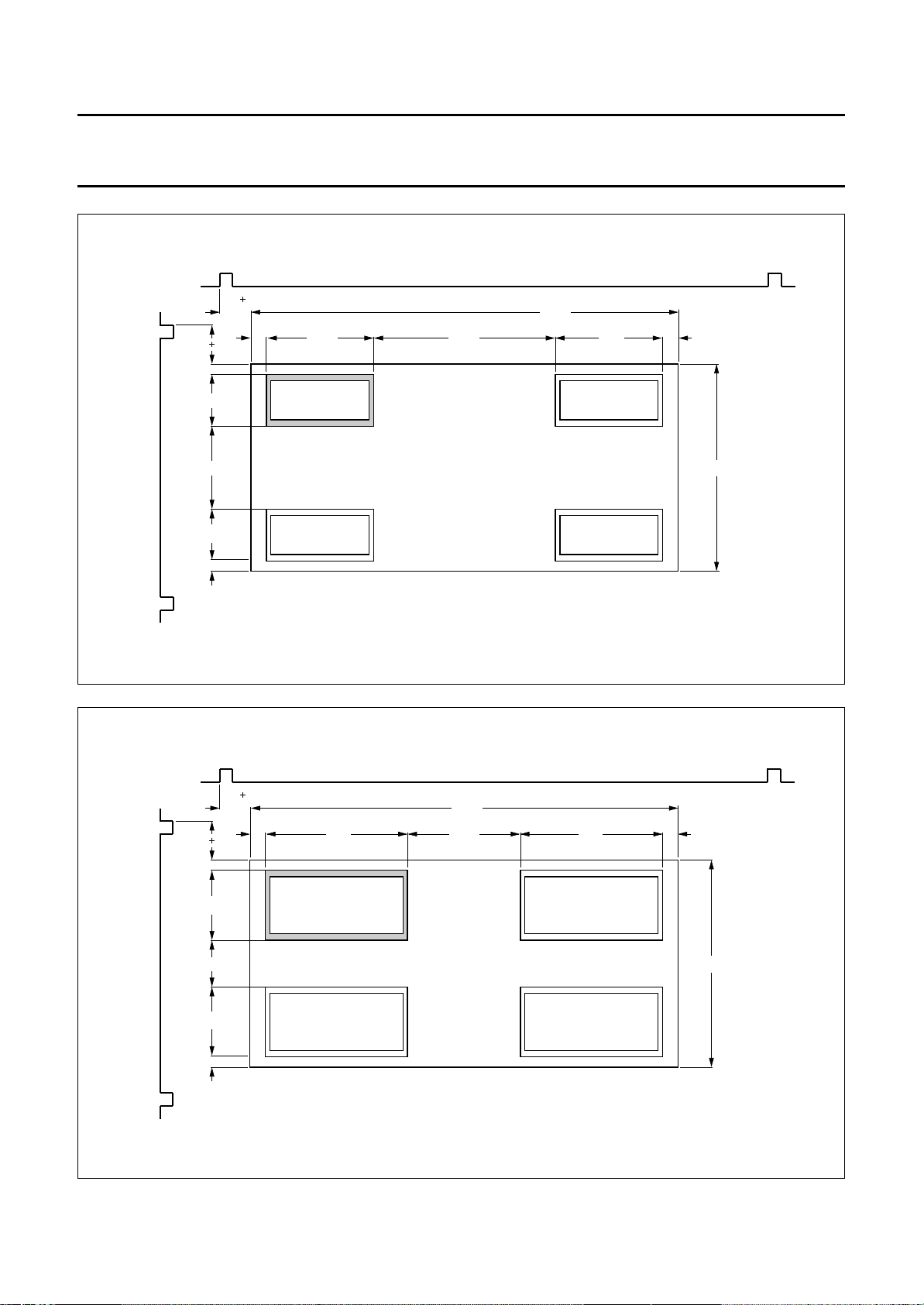
PIP positions
The positions are graphically depicted in Figs 5 to 17.
February 1995 11
Philips Semiconductors Preliminary specification
Picture-in-Picture (PIP) controller for NTSC SAB9075H
handbook, full pagewidth
burstkey
V
sync
11 FT
11
57
92
57
11
36 FT
288
S
Fig.5 Single-PIP, size1⁄16(mode SPS).
672
2416824 168
228
MBE087
handbook, full pagewidth
burstkey
V
sync
11 FT
11
76
54
76
11
36 FT
24
224
176
S
Fig.6 Single-PIP, size1⁄9(mode SPL).
February 1995 12
672
224
24
228
MBE088
 Loading...