

Philips saa9750h DATASHEETS

INTEGRATED CIRCUITS
DATA SH EET
SAA9750H
Camera Digital Signal Processor
(CAMDSP)
Preliminary specification
File under Integrated Circuits, IC02
1996 Feb 16
Philips Semiconductors Preliminary specification
Camera Digital Signal Processor
(CAMDSP)
FEATURES
• Y/C separator for mosaic filter colour CCD which can be
used with PAL or NTSC CCDs with horizontal resolution
of 510, 670, 720 or 768 pixels
• Line sequential colour processing (R−Y) and (B−Y)
• 9 bit input signal (the internal processing is 10-bit)
• Digital feedback clamp control for Y/C separation
• Two 768 × 9 line memories for Y/C separation
• Aperture correction using phase linear filters
• Coring of LOW level signals to reduce noise
• Colour encoder in accordance with the PAL or NTSC
system. Colour subcarrier is made by a discrete time
oscillator (DTO) operating on system clock
• Slew rate controlled outputs for reduction of digital noise
• RGB inputs for title mix
• High accuracy 8 bit DAC outputs for luminance and
chrominance signals
SAA9750H
• Sync Signal Generator (SSG) to generate all necessary
timing signals
• Serial interface for microprocessor control of CAMDSP
settings
• Y and C signals accessible to incorporate digital
features
• Including digital feature functions (mosaic, sepia,
solarization, slice and negative/positive inversion).
GENERAL DESCRIPTION
The Camera Digital Signal Processor (CAMDSP) is
intended for use with a mosaic filter colour CCD. The IC
generates luminance and chrominance signals from the
CCD signal. The device consists of a luminance and colour
separator employing two 768 × 9 line memories, a
PAL/NTSC encoder, a dual 8-bit video DAC, a Sync Signal
Generator (SSG) and a simple serial interface to control
many settings.
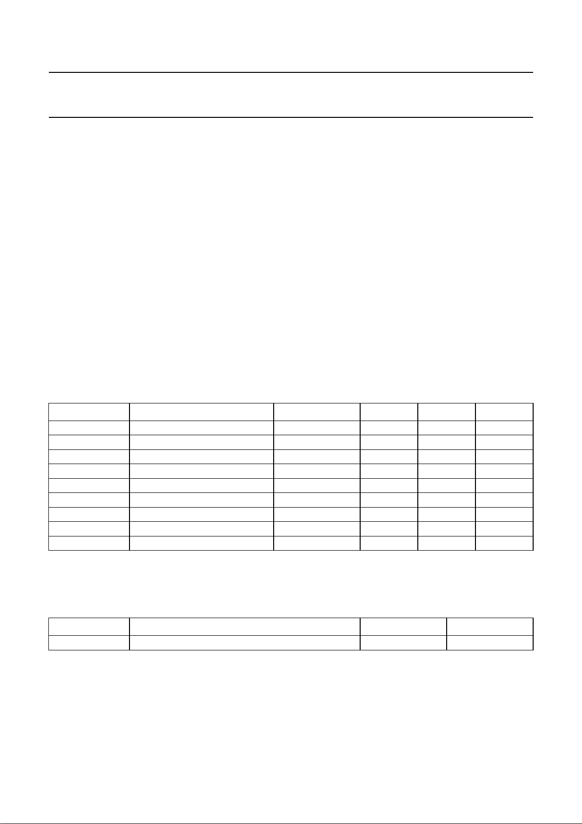
QUICK REFERENCE DATA
SYMBOL PARAMETER MIN. TYP. MAX. UNIT
V
DDA1
V
DDA2
V
DDD1
V
DDD2
V
DDD3
V
IH
V
IL
V
OH
V
OL
T
amb
Y-DAC analog supply voltage (pin 1) 2.7 3.0 3.3 V
C-DAC analog supply voltage (pin 2) 2.7 3.0 3.3 V
digital supply voltage (pin 41) 2.7 3.0 3.3 V
digital supply voltage (pin 53) 2.7 3.0 3.3 V
digital supply voltage (pin 65) 2.7 3.0 3.3 V
HIGH level digital input voltage 0.7V
DDD
LOW level digital input voltage 0 − 0.3V
HIGH level digital output voltage V
DDD
− V
DDD
DDD
V
V
− 0.5 −−V
LOW level digital output voltage −−0.5 V
operating ambient temperature −20 − +70 °C
ORDERING INFORMATION
TYPE
NUMBER
NAME DESCRIPTION VERSION
PACKAGE
SAA9750H LQFP80 plastic low profile quad flat package; 80 leads; body 12 × 12 × 1.4 mm SOT315-1
1996 Feb 16 2
1996 Feb 16 3
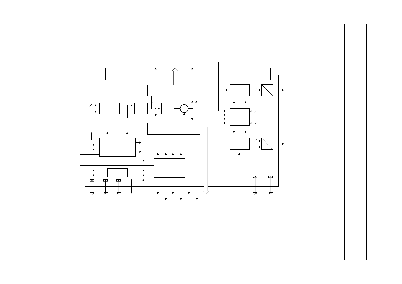
BLOCK DIAGRAM
(CAMDSP)
Philips Semiconductors Preliminary specification
Camera Digital Signal Processor
CDS0 to
CDS
CPOB
CLAMP
VRST
HRST
CLK1
CLK2
CS
CK
DDD2
V
DDD3
DDD1
415365
UV
V
V
SAA9750H
9
8
68 to 76
62
61
CLAMP
settings
30
31
32
DI
51
52
66
67
V
SSD2
CLAMP
Y settings
MICROPROCESSOR
64
54
V
SSD3
X0H
C settings
INTERFACE
CLOCK
42
V
SSD1
FIFO
768 × 9
ENCODER
settings
SSG
settings
TEST1 TEST2
X1H
CSYNC HD FLD SYNCI V
UV0 to
SEL
29 20 8 9 10 11 7 1 2
UV
7
21 to 28
8
C PROCESSING
FIFO
768 × 9
Y PROCESSING
SYNC SIGNAL
GENERATOR
59
5577 6 56 63
VD CP2 HSYNC
X2H
+
58
57
Y0 to Y
R
8
33 to 40
B
LSWTSWWCLIP
G
ENCODER
UV
ENC
TITLE
SWITCH
Y
ENC
DELAY
7
V
title mix
title mix
sync
60
V
DDA1
8
8
8
8
SSA1VSSA2
DDA2
3
A
D
5
12 to 19
43 to 50
80
A
D
78
479
C
V
refC
UV
UV
Y
ENC7
Y
ENC0
Y
OUT
V
refY
MHA302
OUT
ENC0
ENC7
to
to
handbook, full pagewidth
Fig.1 Block diagram.
SAA9750H
Philips Semiconductors Preliminary specification
Camera Digital Signal Processor
SAA9750H
(CAMDSP)
PINNING
SYMBOL PIN INPUT/OUTPUT ANALOG/DIGITAL DESCRIPTION
V
DDA1
V
DDA2
C
OUT
V
SSA1
V
refC
TEST2 6 input digital test 2 pin
LSW 7 input digital line switch for SECAM
TSW 8 input digital title memory switch
R 9 input digital title memory colour (red)
G 10 input digital title memory colour (green)
B 11 input digital title memory colour (blue)
UV
ENC0
UV
ENC1
UV
ENC2
UV
ENC3
UV
ENC4
UV
ENC5
UV
ENC6
UV
ENC7
WCLIP 20 output digital white-clip
UV
7
UV
6
UV
5
UV
4
UV
3
UV
2
UV
1
UV
0
UV
SEL
CS 30 input digital microprocessor interface (chip select)
CK 31 input digital microprocessor interface (clock)
DI 32 input digital microprocessor interface (data input)
Y
0
Y
1
Y
2
Y
3
Y
4
Y
5
Y
6
Y
7
1 supply − analog supply voltage 1 for Y-DAC
2 supply − analog supply voltage 2 for C-DAC
3 output analog C-DAC output
4 supply − analog ground 1 for C-DAC
5 −− C-DAC decoupling voltage
12 input digital B−Y and R−Y signal to encoder (LSB)
13 input digital B−Y and R−Y signal to encoder
14 input digital B−Y and R−Y signal to encoder
15 input digital B−Y and R−Y signal to encoder
16 input digital B−Y and R−Y signal to encoder
17 input digital B−Y and R−Y signal to encoder
18 input digital B−Y and R−Y signal to encoder
19 input digital B−Y and R−Y signal to encoder (MSB)
21 output digital time multiplexed B−Y and R−Y (MSB)
22 output digital time multiplexed B−Y and R−Y
23 output digital time multiplexed B−Y and R−Y
24 output digital time multiplexed B−Y and R−Y
25 output digital time multiplexed B−Y and R−Y
26 output digital time multiplexed B−Y and R−Y
27 output digital time multiplexed B−Y and R−Y
28 output digital time multiplexed B−Y and R−Y (LSB)
29 output digital B−Y or R−Y active at UV output
33 output digital luminance signal (LSB)
34 output digital luminance signal
35 output digital luminance signal
36 output digital luminance signal
37 output digital luminance signal
38 output digital luminance signal
39 output digital luminance signal
40 output digital luminance signal (MSB)
1996 Feb 16 4
Philips Semiconductors Preliminary specification
Camera Digital Signal Processor
SAA9750H
(CAMDSP)
SYMBOL PIN INPUT/OUTPUT ANALOG/DIGITAL DESCRIPTION
V
DDD1
V
SSD1
Y
ENC7
Y
ENC6
Y
ENC5
Y
ENC4
Y
ENC3
Y
ENC2
Y
ENC1
Y
ENC0
VRST 51 input digital external VD (vertical drive)
HRST 52 input digital external HD (horizontal drive)
V
DDD3
V
SSD3
VD 55 output digital VD timing for PPG IC
HD 56 output digital HD timing for PPG IC
FLD 57 output digital field pulse output
HSYNC 58 output digital horizontal timing for YC processing
CSYNC 59 output digital composite sync pulse
SYNCI 60 input digital sync input for bypass mode
CLAMP 61 output (3-state) digital clamp voltage control
CPOB 62 input digital optical black pulse
CP2 63 output digital clamping pulse
V
SSD2
V
DDD2
CLK1 66 input digital clock 1
CLK2 67 input digital clock 2
CDS
0
CDS
1
CDS
2
CDS
3
CDS
4
CDS
5
CDS
6
CDS
7
CDS
8
TEST1 77 input digital test 1 pin
V
refY
V
SSA2
Y
OUT
41 supply − digital supply voltage 1
42 supply − digital ground 1
43 input digital luminance signal to encoder (MSB)
44 input digital luminance signal to encoder
45 input digital luminance signal to encoder
46 input digital luminance signal to encoder
47 input digital luminance signal to encoder
48 input digital luminance signal to encoder
49 input digital luminance signal to encoder
50 input digital luminance signal to encoder (LSB)
53 supply − digital supply voltage 3
54 supply − digital ground 3
64 supply − digital ground 2
65 supply − digital supply voltage 2
68 input digital CDS signal (LSB)
69 input digital CDS signal
70 input digital CDS signal
71 input digital CDS signal
72 input digital CDS signal
73 input digital CDS signal
74 input digital CDS signal
75 input digital CDS signal
76 input digital CDS signal (MSB)
78 −− Y-DAC decoupling voltage
79 supply − analog ground 2 for Y-DAC
80 output analog Y-DAC output
1996 Feb 16 5

Philips Semiconductors Preliminary specification
Camera Digital Signal Processor
(CAMDSP)
OUTVSSA2VrefY
handbook, full pagewidth
V
DDA1
V
DDA2
C
OUT
V
SSA1
V
refC
TEST2
LSW
TSW
R
G
B
UV
ENC0
UV
ENC1
UV
ENC2
UV
ENC3
UV
ENC4
UV
ENC5
UV
ENC6
UV
ENC7
WCLIP
Y
80
79
1
2
3
4
5
6
7
8
9
10
11
12
13
14
15
16
17
18
19
20
21
22
UV7UV6UV5UV4UV3UV2UV1UV
TEST1
CDS8CDS7CDS6CDS5CDS4CDS3CDS2CDS1CDS0CLK2
78
77
76
75
74
23
24
25
26
27
73
28
0
72
71
SAA9750H
29
30
CS
SEL
UV
70
31
CK
DDD2VSSD2
CLK1
V
69
68
67
66
65
64
32
33
34
35
36
37
DI
Y0Y1Y2Y3Y4Y5Y6Y
CP2
63
38
SAA9750H
CPOB
CLAMP
62
61
60
59
58
57
56
55
54
53
52
51
50
49
48
47
46
45
44
43
42
41
MHA301
39
40
7
SYNCI
CSYNC
HSYNC
FLD
HD
VD
V
SSD3
V
DDD3
HRST
VRST
Y
ENC0
Y
ENC1
Y
ENC2
Y
ENC3
Y
ENC4
Y
ENC5
Y
ENC6
Y
ENC7
V
SSD1
V
DDD1
Fig.2 Pin configuration.
1996 Feb 16 6
Philips Semiconductors Preliminary specification
Camera Digital Signal Processor
(CAMDSP)
FUNCTIONAL DESCRIPTION
The Camera Digital Signal Processor (CAMDSP) is
intended for use with a mosaic filter colour CCD.
The input signal is an 8-bit or 9-bit digitized CCD signal.
After AGC and gamma correction, clamping of the input
signal is achieved by feedback clamp level control.
In the luminance processing, symmetrical horizontal and
vertical aperture correction are carried out. Coring is also
carried out to reduce noise at LOW signal levels. In the
chrominance processing, white balance control and matrix
control is adjustable. A false colour correction circuit
reduces aliasing of high frequency input signals.
A white-clip makes the colour white at highlights.
In the encoder part, the colour encoder subcarrier is made
by the discrete time oscillator thus eliminating the use of an
extra crystal. The subcarrier frequency for PAL or NTSC is
selectable. The encoding can be in PAL or NTSC format.
SAA9750H
The encoded signal is output via separate 8-bit
digital-to-analog converters (DACs) for luminance and
chrominance. In the event of SECAM the output is a line
sequential −(R−Y)/(B−Y) signal. A line memory interface
allows for mixing of RGB signals in the main signal.
The encoder can be bypassed completely, in this event
only the title mix is carried out before digital-to-analog
conversion.
The SSG generates all necessary timing signals. Timing
signals for external devices NTSC, PAL and SECAM are
also made. The SSG can be locked to an external video
source.
CAMDSP can operate with 510H, 670H, 720H and 768H
colour mosaic CCDs both PAL and NTSC type. In the
510H CCD application the upsampling clock is used for the
encoder part, therefore two clock frequencies (f
are required.
and 2fs)
s
LIMITING VALUES
In accordance with the Absolute Maximum Rating System (IEC 134).
SYMBOL PARAMETER CONDITIONS MIN. MAX. UNIT
V
V
P
V
V
T
T
V
I
latch
DDD
DDA
tot
I
O
stg
amb
es
digital supply voltage −0.5 +5.0 V
analog supply voltage −0.5 +5.0 V
total power dissipation − 500 mW
digital input voltage −0.5 V
digital output voltage −0.5 V
DDD
DDD
+ 0.5 V
+ 0.5 V
storage temperature −65 +150 °C
operating ambient temperature −20 +70 °C
electrostatic handling note 1 −2000 +2000 V
latch-up protection current 100 − mA
Note
1. Equivalent to discharging a 100 pF capacitor via a 1.5 kΩ series resistor.
THERMAL CHARACTERISTICS
SYMBOL PARAMETER VALUE UNIT
R
th j-a
thermal resistance from junction to ambient in free air 57 K/W
1996 Feb 16 7

Philips Semiconductors Preliminary specification
Camera Digital Signal Processor
SAA9750H
(CAMDSP)
DC CHARACTERISTICS
V
= 2.7 to 3.3 V; T
DD
SYMBOL PARAMETER CONDITIONS MIN. TYP. MAX. UNIT
I
DD
supply current note 1 − 60 150 mA
Inputs: LSW, TSW, R, G, B, UV
CLK2, CDS
V
IH
V
IL
I
IH
I
IL
to CDS7, TEST1 and TEST2
0
HIGH level input voltage 0.7V
LOW level input voltage −−0.3V
HIGH level input current VIH=V
LOW level input current VIL=V
Outputs: WCLIP, UV
V
OH
V
OL
HIGH level output voltage IOH= −20 µAV
LOW level output voltage IOL= +20 µA −−0.1 V
Output: CLAMP (3-state output)
V
OH
V
OL
I
TL
HIGH level output voltage IOH= −20 µAV
LOW level output voltage IOL= +20 µA −−0.1 V
3-state leakage current VIH=VDD; VIL=V
= −20 to +70 °C; unless otherwise specified.
amb
to UV7, UV
0
to UV
ENC0
, Y0to Y7, VD, HD, FLD, HSYNC, CSYNC and CP2
SEL
, CS, CK, DI, Y
ENC7
DD
SS
I
= −2mA VDD− 0.5 −−V
OH
=+2mA −−0.5 V
I
OL
I
= −8mA VDD− 0.5 −−V
OH
=+8mA −−0.5 V
I
OL
ENC0
SS
to Y
, VRST, HRST, SYNCI, CPOB, CLK1,
ENC7
−−V
DD
DD
V
−−1µA
−−−1µA
− 0.1 −−V
DD
− 0.1 −−V
DD
−−±5µA
Note
1. 510H PAL; V
= 3 V; DAC RL=2kΩ.
DD
DAC CHARACTERISTICS
V
DD
= 3.0 V; T
= +25 °C; RL= open-circuit; unless otherwise specified.
amb
SYMBOL PARAMETER MIN. TYP. MAX. UNIT
Outputs: Y
f
Cmax
and C
OUT
OUT
conversion frequency speed 20 −−MHz
INL DC integral linearity error −0.5 − +0.5 LSB
DNL DC differential linearity error −0.5 − +0.5 LSB
V
O(p-p)
R
O
full scale output except sync (peak-to-peak value) 1.61 1.66 1.72 V
internal series output resistance − 75 −Ω
1996 Feb 16 8
 Loading...