


INTEGRATED CIRCUITS
DATA SH EET
SAA9740H
Advanced Auto Control Function
(A2CF)
Product specification
Supersedes data of 1996 Jan 30
File under Integrated Circuits, IC02
1996 Oct 10

Philips Semiconductors Product specification
Advanced Auto Control Function (A2CF) SAA9740H
FEATURES
• One chip full digital Auto Focus (AF), Auto Exposure
(AE) and Auto White Balance (AWB)
• Possible to use NTSC and PAL CCD with horizontal
resolution of 510, 670, 720 or 768 pixels
• No manual adjustment
• One microprocessor system commonly used with
CAMera Digital Signal Processor (CAMDSP)
SAA9750H
• 8-bit parallel microprocessor interface
• LQFP64 package (0.5 mm pitch)
• Single 3 V power supply.
Auto Focus features
• Video AF system
• Two windows system (a small centre and large window)
• The window size and place are microprocessor
controlled
th
• Including 5
order IIR digital high-pass filter
• Line peak accumulation in the large window
• High-pass filter’s output accumulation in one field.
Auto Exposure features
• 5 windows accumulation
• Calculation of white-clip by centre window
• Possible to control size and place of the centre windows
by the light condition with microprocessor.
Auto White Balance features
• Mono colour detection
• Accumulation of UV data in the corresponding UV
quadrant
• Green and Magenta elimination gate
• Luminance gate for detecting white
• UV limiter
• White-clip detection/counter.
GENERAL DESCRIPTION
The Advanced Auto Control Function (A2CF) is to be used
for a colour CCD camera system. This IC can realize AWB,
AF and AE with a microprocessor. This device consists of
an input data selector, a parallel 8-bit microprocessor
interface, a data accumulator, a window generator, a
command decoder and AWB, AF, AE for each processing
block.
QUICK REFERENCE DATA
SYMBOL PARAMETER MIN. TYP. MAX. UNIT
V
DD
V
IL
V
IH
V
OL
V
OH
T
amb
digital supply voltage (pins 6, 18 and 47) 2.7 3.0 3.3 V
LOW level digital input voltage 0 − 0.3V
HIGH level digital input voltage 0.7V
DD
− V
DD
DD
V
V
LOW level digital output voltage −−0.5 V
HIGH level digital output voltage VDD− 0.5 −−V
operating ambient temperature −20 − +70 °C
ORDERING INFORMATION
TYPE
NUMBER
NAME DESCRIPTION VERSION
PACKAGE
SAA9740H LQFP64 plastic low profile quad flat package; 64 leads; body 10 × 10 × 1.4 mm SOT314-2
1996 Oct 10 2
Philips Semiconductors Product specification
Advanced Auto Control Function (A2CF) SAA9740H
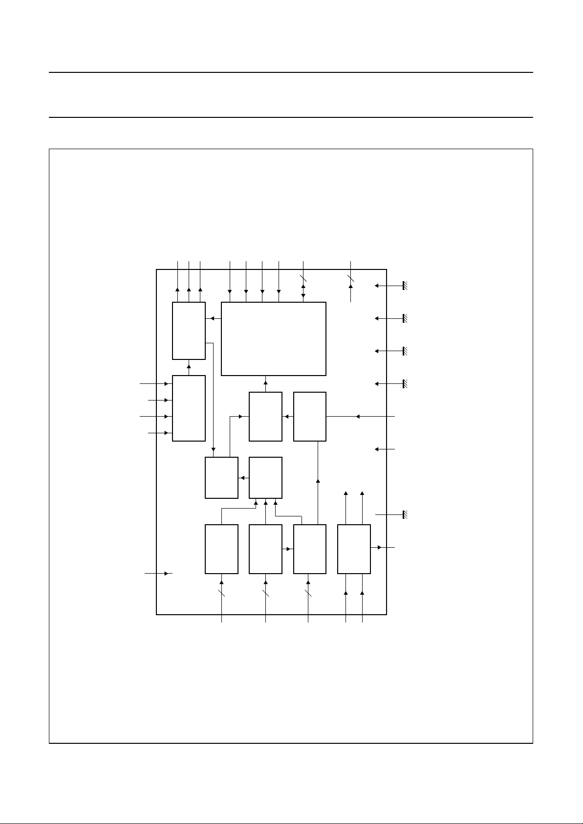
BLOCK DIAGRAM
to
LWDB
WDMNT
WDINT
ASTB
WRB
RDB
RSTB28IO7 to IO0
TSTOUT7
TSTOUT1
MHA286
UV_SEL
HSYNC
VD
HD
DD3
to V
DD1
V
+3 V
373632
34 33 35 86, 18, 47
WINDOW
GENERATOR
H/V
COUNTER
SAA9740H
57 to 50
31
30
enable signals
18-BIT
ADDER
AUTO
FOCUS
8
29
20 to 27
INTERFACE
MICROPROCESSOR
REGISTER
PEAK
HOLD
AUTO
EXPOSURE
5
61 to 64, 1
AUTO
16 to 9
8
CLIP
WHITE
WHITE
BALANCE
8
7
39, 38, 45 to 41
CLK1
1/2 CLK1
CLOCK
GENERATOR
48
60
5
TST1
4
TSTIN3
3
TSTIN2
2
TSTIN1
17
WCLIP
58
SCAN_T
SS5
to V
SS1
7, 19 46, 49, 59
V
40
CLK2OUT
Fig.1 Block diagram.
to
CDS7
CDS0
handbook, full pagewidth
Y7 to Y3
1996 Oct 10 3
UV7 to UV0
CLK1
AMSAL

Philips Semiconductors Product specification
Advanced Auto Control Function (A2CF) SAA9740H
PINNING
SYMBOL PIN TYPE DESCRIPTION
Y3 1 input Y input from SAA9750H (CAMDSP) (LSB)
TSTIN1 2 input input pin for test
TSTIN2 3 input input pin for test
TSTIN3 4 input input pin for test
TST1 5 input input pin for test
V
DD1
V
SS1
UV_SEL 8 input UV select input from SAA9750H (CAMDSP)
UV0 9 input UV input from SAA9750H (CAMDSP) (LSB)
UV1 10 input UV input from SAA9750H (CAMDSP)
UV2 11 input UV input from SAA9750H (CAMDSP)
UV3 12 input UV input from SAA9750H (CAMDSP)
UV4 13 input UV input from SAA9750H (CAMDSP)
UV5 14 input UV input from SAA9750H (CAMDSP)
UV6 15 input UV input from SAA9750H (CAMDSP)
UV7 16 input UV input from SAA9750H (CAMDSP) (MSB)
WCLIP 17 input white-clip input from SAA9750H (CAMDSP)
V
DD2
V
SS2
IO7 20 bidirectional microprocessor interface (MSB)
IO6 21 bidirectional microprocessor interface
IO5 22 bidirectional microprocessor interface
IO4 23 bidirectional microprocessor interface
IO3 24 bidirectional microprocessor interface
IO2 25 bidirectional microprocessor interface
IO1 26 bidirectional microprocessor interface
IO0 27 bidirectional microprocessor interface (LSB)
RSTB 28 input system reset
RDB 29 input read control from microprocessor
WRB 30 input write control from microprocessor
ASTB 31 input address set from microprocessor
WDINT 32 output window interrupt
VD 33 input V-drive signal input
HD 34 input H-drive signal input
HSYNC 35 input HSYNC input
WDMNT 36 output window monitor for test (open-drain)
LWDB 37 output large window for test (open-drain)
TSTOUT6 38 output output pin for test
TSTOUT7 39 output output pin for test
CLK2OUT 40 output output pin of internal clock (open-drain)
6 − digital supply voltage
7 − ground
18 − digital supply voltage
19 − ground
1996 Oct 10 4

Philips Semiconductors Product specification
Advanced Auto Control Function (A2CF) SAA9740H
SYMBOL PIN TYPE DESCRIPTION
TSTOUT1 41 output output pin for test
TSTOUT2 42 output output pin for test
TSTOUT3 43 output output pin for test
TSTOUT4 44 output output pin for test
TSTOUT5 45 output output pin for test
V
SS3
V
DD3
CLK1 48 input clock
V
SS4
CDS0 50 input CDS input from ADC (LSB)
CDS1 51 input CDS input from ADC
CDS2 52 input CDS input from ADC
CDS3 53 input CDS input from ADC
CDS4 54 input CDS input from ADC
CDS5 55 input CDS input from ADC
CDS6 56 input CDS input from ADC
CDS7 57 input CDS input from ADC (MSB)
SCAN_T 58 input test control for scan test
V
SS5
AMSAL 60 input for testing
Y7 61 input Y input from SAA9750H (CAMDSP) (MSB)
Y6 62 input Y input from SAA9750H (CAMDSP)
Y5 63 input Y input from SAA9750H (CAMDSP)
Y4 64 input Y input from SAA9750H (CAMDSP)
46 − ground
47 − digital supply voltage
49 − ground
59 − ground
1996 Oct 10 5
Philips Semiconductors Product specification
Advanced Auto Control Function (A2CF) SAA9740H
handbook, full pagewidth
Y3
TSTIN1
TSTIN2
TSTIN3
TST1
V
DD1
V
SS1
UV_SEL
UV0
UV1
UV2
UV3
UV4
UV5
UV6
UV7
Y4
Y5
Y6
Y7
64
63
62
61
1
2
3
4
5
6
7
8
AMSAL
60
SS5
V
59
SCAN_T
CDS7
58
57
CDS6
56
CDS5
55
CDS4
54
CDS3
53
CDS2
52
CDS1
51
SAA9740H
9
10
11
12
13
14
15
16
CDS0
50
SS4
V
49
48
47
46
45
44
43
42
41
40
39
38
37
36
35
34
33
CLK1
V
DD3
V
SS3
TSTOUT5
TSTOUT4
TSTOUT3
TSTOUT2
TSTOUT1
CLK2OUT
TSTOUT7
TSTOUT6
LWDB
WDMNT
HSYNC
HD
VD
17
18
19
20
21
22
23
IO4
IO5
IO6
IO7
SS2
DD2
V
V
WCLIP
Fig.2 Pin configuration.
1996 Oct 10 6
24
IO3
25
IO2
26
IO1
27
IO0
28
RSTB
29
RDB
30
WRB
31
ASTB
32
WDINT
MHA285
Philips Semiconductors Product specification
Advanced Auto Control Function (A2CF) SAA9740H
FUNCTIONAL DESCRIPTION
The Advanced Auto Control Function (A2CF) will be used
for colour CCD camera systems.
The input signals are CDS (AF data) from 8-bit ADC,
Y (for AE, 5-bit) and UV (for AWB, 8-bit) data as the output
of SAA9750H (CAMDSP) and they are fed into the A2CF.
After being processed in the A2CF, corresponding data
are led into the microprocessor.
Together with the zoom encoder and focus sensor output
the microprocessor does the following control with the data
of A2CF:
• Control focus motor
• Control iris, AGC (via DAC) and high speed shutter
• Send the control data to SAA9750H (CAMDSP) via
serial bus.
CLK1 is depending on the CCD type. To cope with the
different CCD clocks, some reference data have to be set
by the microprocessor.
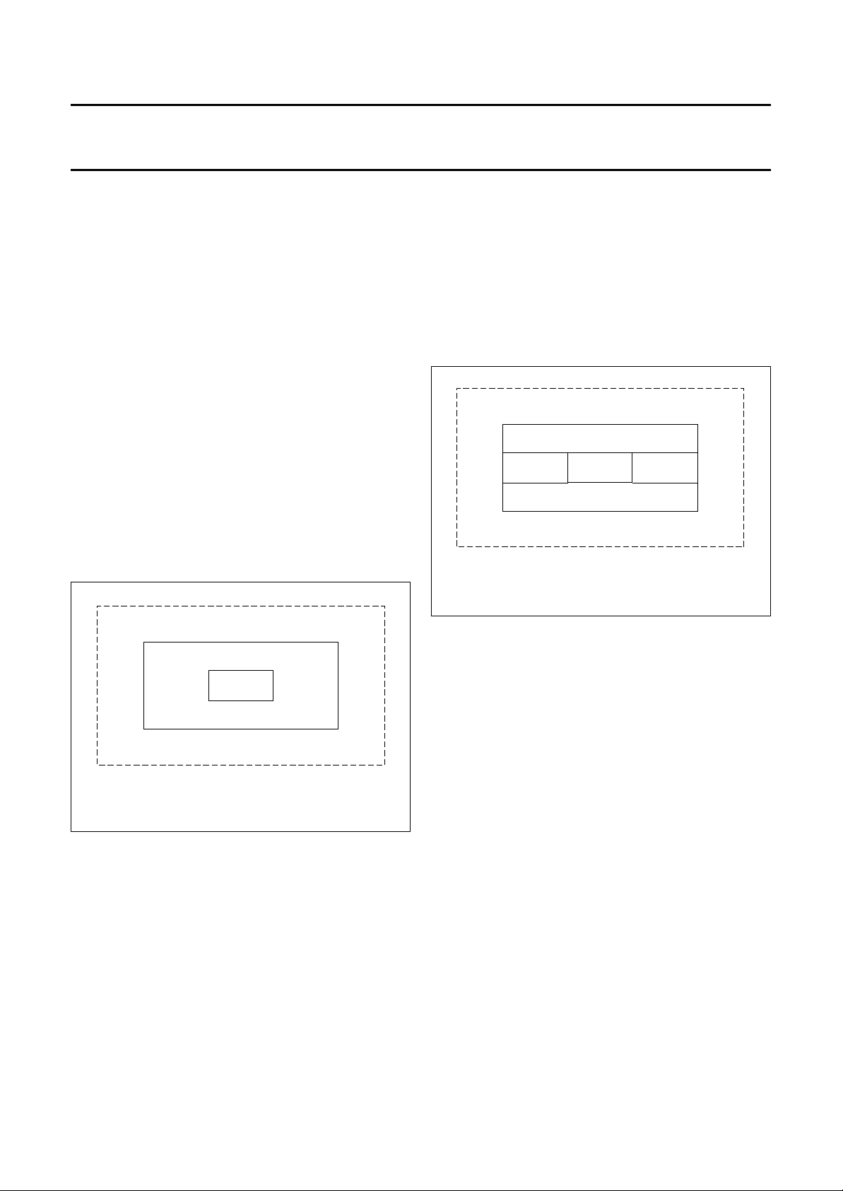
AF system
handbook, halfpage
active video
This maximum focus value is accumulated in the AF
window (see Fig.3) by the 18-bit adder. The values in the
large window are stored in REG2 (see Table 7) and those
in the small window are stored in REG3 (see Table 7).
Which data is used is dependent on the software (see
Tables 6 and 7). Besides this accumulation, line peak
accumulation is also done. This data is the maximum value
in one field and is stored in REG0 (see Table 7).
AE system
handbook, halfpage
1
324
5
active video
MHA288
Fig.4 AE window.
large window
centre
window
MHA287
Fig.3 AF window.
Digital CDS signals CDS7 to CDS0 which come after
AGC, gamma processing and ADC are fed into A2CF.
This 8-bit data is shifted to the most suitable 6-bit data for
AF processing by microprocessor. For example, when the
MSB of them is ‘1’ then the 6-bit data is shifted by the
microprocessor to CDS7 to CDS2
(not CDS6 to CDS1 or CDS5 to CDS0; see Table 4). After
AF shifting the signals go through an LPF and they are
down sampled. The down sampling is done by CLK2
(CLK1/2). In order to detect the high frequency component
for AF processing, one HPF is added. This output is the
focus value. Next peak hold block is for acquiring
maximum focus value of every line in one field.
5-bit Y signals Y7 to Y3 which come from SAA9750H are
fed into A2CF for AE processing. This signal is internally
extended to 6 bits by adding a ‘0’ as new MSB. Next they
go through an LPF and they are down sampled in the
same way as AF processing. In order to prevent overflow
of the 18-bit adder block, 2 modes exist (see Table 4).
The first is H decimation is on oroff. If H decimation is on,
then the data for AE processing is available in every other
line. The second mode is that the data for AE processing
1
is shifted to
⁄2 or not. If the data is shifted to1⁄2, it is done
before down sampling and before the data going to the
18-bit adder becomes1⁄2. Both these modes are controlled
by the microprocessor. In AE mode there are 5 windows
as shown in Fig.4. These windows are controlled by the
microprocessor. The accumulation data in window 1 to
window 5 is respectively stored in REG1 to REG5 (see
Table 7). The white-clip count data in the centre window is
stored to the lower 5 bits of REG0 (see Table 7).
The upper 3 bits of REG0 is the overflow information in the
18-bit adder (see Table 7).
1996 Oct 10 7
Philips Semiconductors Product specification
Advanced Auto Control Function (A2CF) SAA9740H
AWB system
8-bit UV signals UV[7] to UV[0] which come from the
SAA9750H (CAMDSP) are fed into the A2CF for AWB
processing. First the 8-bit data is limited to 6-bits because
the necessary data for AWB processing is around the
white colour signal. Then these signals go through an LPF
and they are down sampled. They are separated to U and
V signals by using UV_SEL coming from SAA9750H
(CAMDSP). As shown in Table 1, in the large window
these signals are compared with the threshold that is set
by the microprocessor. If the conditions shown in Fig.8 are
valid, the data is available for AWB processing. If the
conditions aren’t valid, the data is ignored. The available
data in the first to the 4th quadrant are stored in
mode (see Table 4) is for detecting whether the picture is
mono colour or not. If the AWB (B − Y) or AWB (R − Y) or
AWB (∆) (see Table 4) mode is active and white-clip or
AWB limited (as mentioned above), then the counts of
them are stored in the lower 5 bits of REG0 (see Table 7).
In the AWB Y mode the lower 4 bits of REG0 are contrast
peak data in one field and the 4th bit is the overflow
information of the AF (see Table 7).
Microprocessor interface
8-bit data bus and 3 control ports are prepared (WRB,
RDB and ASTB) for microprocessor interface in A2CF for
quick data access instead of serial bus. A2CF has 11 read
commands and 13 write commands.
respectively REG1 to REG4 (see Table 7). The AWB (∆)
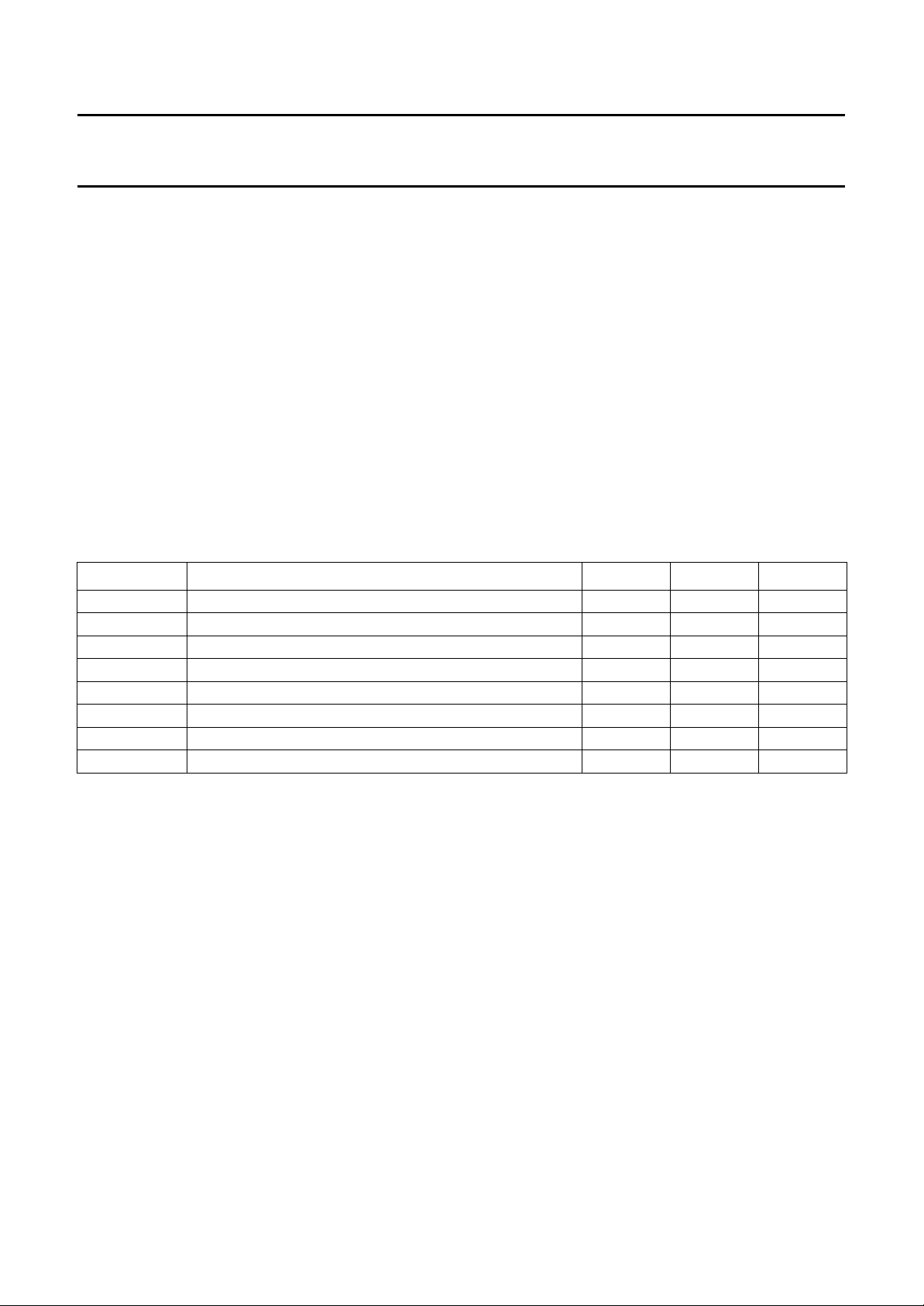
LIMITING VALUES
In accordance with the Absolute Maximum Rating System (IEC 134).
SYMBOL PARAMETER MIN. MAX. UNIT
V
DD
P
tot
V
I
V
O
T
stg
T
amb
V
es
supply voltage −0.5 +5.0 V
total power dissipation − 83 mW
input voltage −0.5 VDD+ 0.5 V
output voltage −0.5 VDD+ 0.5 V
storage temperature −65 +150 °C
operating ambient temperature −20 +70 °C
electrostatic handling; note 1 −2000 +2000 V
LTCH latch-up protection 100 − mA
Note
1. Equivalent to discharging a 100 pF capacitor through a 1.5 kΩ series resistor.
1996 Oct 10 8
 Loading...