

Philips SAA8122A Datasheet

1. Description
SAA8122A
Digital Still Camera Processor (ImagIC family)
Rev. 01 — 20 April 2000 Objective specification
The DSC SAA8122A is a high performance, low power, single-chip Million
Instructions Per Second (MIPS) based signal processor, part of the ImagIC family,
which is dedicated to image processing, compression, formatting and storage. The
DSC SAA8122A is optimized for use with Philips range of CCDs (e.g: FXA1022,
2 Mpixels CCD), V-driver (TDA9991), CDS/PGA/ADC (TDA9952), allowing easy
implementation of a complete system solution and fast development of high
performance consumer digital still cameras.
The SAA8122A is designed as a single-chip device, able to perform all treatments
and connections required for a wide range of Digital Still Cameras. Its embedded
RISC CPU, for which the development environment is available, enables shorter
development and validation cycles, as well as faster feature upgrade. Since one of
the main objectives of the SAA8122A is addressing a wide range of CCD sensors, a
DSP (with advanced embedded algorithm) forcamera signal processing is integrated
with a high level of programmability for pulses generation.
2. Features
The JPEG core is hardware based in order to allow high-speed image data
compression.
c
c
2.1 General
■ Supports a wide range of progressive CCDs (VGA, SVGA, QGA, XGA, EQGA),
■ Performs an advanced RGB to YUV conversion
■ Includes a smart measurement unit to speed up the control loop (focus,auto white
■ Supports a wide range of LCD and TV formats (both NTSC and PAL) with text
■ Includes an embedded JPEG encoder/decoder unit
■ Includes a MIPS PR3001 CPU, running at a frequency in a range from
■ PRISC compatible PI-bus architecture, interrupt, power management, clock and
■ Includes a dedicated video bus supporting SDRAM memory for picture storage
with RGB Bayer filters up to 2 Mpixels
balance, etc.)
insertion features
12 to 28 MHz
reset architectures

Philips Semiconductors
■ Interface to ROM, DRAM, SRAM, flash and PC Card [Compact Flash and SSFDC
■ Integrated general purpose peripheral units like a UART, timers, an I2C-bus
■ Includes USB and RS-232C communication interfaces.
2.2 External interfaces
■ Two UART (RS-232) data ports with DMA capabilities (≤187.5 kbit/s) including
■ 32 general purpose, bidirectional I/O interface pins, the first 8 bits may also be
■ Two PWM outputs (8-bit resolution).
2.3 CPU related features
■ 32-bit PR3001 core
■ 1-kbyte data cache and 4-kbyte instruction cache
■ Programmable low-power mode, including wake-up on interrupt
■ Memory management unit [Translation Lookaside Buffer (TLB)]
■ Two built in 24-bit general purpose timers and one 24-bit watchdog timer
■ Real-time clock unit (active in sleep mode)
■ On-chip 8-kbyte SRAM for storing code which needs fast execution
■ Platform software based on real-time pSOS (plug-in Silicon Operating System).
SAA8122A
Digital Still Camera Processor (ImagIC family)
(SmartMedia)]
transceiver, ADC converters, RTC and I/O ports
hardware flow control RxD, TxD, RTS, CTS for modem support
used as interrupt inputs
2.4 DSP features
■ Advanced colour reconstruction
■ Programmable digital filters for noise reduction and contour enhancement
■ 16 programmable measurement windows allowing to perform the measurements
necessary for exposure, white balance and focus adjustment in a DSC system;
available measurement outputs for exposure, white balance and focus control.
2.5 Pulse pattern generator features
■ Programmable through dedicated PC-software, allowing to drive all CCDs
currently present in the market, as well as CDS/AGC/ADC chips: up to
8 × 8 kpixels.
2.6 JPEG
■ Fully ISO10918 compliant
■ Supports Tiff, Exif 2.1, DCF & DPOF
■ Quick compression (4 images/s for a 1.3 Mpixels resolution).
2.7 USB interface
■ Fully compatible with USB.
9397 750 07048
Objective specification Rev. 01 — 20 April 2000 2 of 26
© Philips Electronics N.V. 2000. All rights reserved.

Philips Semiconductors
2.8 Card interfaces
■ Compatible with all SSFDC/CF cards on the market.
2.9 Bus
■ Bus structure allows for parallel processing depending on software
implementation, allowing easy system optimization.
2.10 SDRAM interface features
■ Supports up to 128 Mbyte of SDRAM and 16-bit wide addressses
■ Bus speed: 1 or 2 times CCD pixel clock
■ 32-bit bus width.
3. Quick reference data
Table 1: Quick reference data
Symbol Parameter Conditions Min Typ Max Unit
V
DDD
V
DDA
I
P
V
I
V
O
T
amb
f
clk
[1] The supplies considered as digital supply (V
[2] The supplies considered as analog supply (V
V
DDA(ADC)
[3] Including voltage on outputs in 3-state mode; only valid when supply voltage is present.
SAA8122A
Digital Still Camera Processor (ImagIC family)
DDD
DDA(SPLL)
, V
DDA(LCDG)
[1]
3 3.3 3.6 V
[2]
3 3.3 3.6 V
[3]
0 − 5.5 V
, V
DDD(RTC)
, V
DDA(PLL)
, V
DDA(LCDB)
.
, V
DDA(BG)
, V
DDA(DLL)
DDD
DDD
, V
.
V
V
DDA(PPG1)
digital supply voltage
analog supply current
total supply current f
=25MHz − 360 560 mA
clk
input voltage
general 0 − V
5 V tolerant cells only
output voltage output active 0 − V
ambient temperature 0 25 70 °C
clock frequency − 25 27 MHz
) are: V
DDD
) are: V
, V
DDA(OUTPUT1)
, V
DDA(OUTPUT2)
, V
DDA(LCDR)
DDA
,
4. Ordering information
Table 2: Ordering information
Type number Package
Name Description Version
SAA8122AEL LFBGA324 plastic low profile fine-pitch ball grid array package; 324 balls;
body 16 × 16 × 1.2 mm
9397 750 07048
Objective specification Rev. 01 — 20 April 2000 3 of 26
© Philips Electronics N.V. 2000. All rights reserved.
SOT571-1

This text is here in white to force landscape pages to be rotated correctly when browsing through the pdf in the Acrobat reader.This text is here in
white to force landscape pages to be rotated correctly when browsing through the pdf in the Acrobat reader.This text is here inThis text is here in
white to force landscape pages to be rotated correctly when browsing through the pdf in the Acrobat reader. white to force landscape pages to be ...
9397 750 07048
Objective specification Rev. 01 — 20 April 2000 4 of 26
PC-CARD
CONTROLLER
DRAM
MEMORY
CONTROLLER
STATIC
MEMORY
CONTROLLER
PERIPHERAL
CONTROLLER
TCB
5. Block diagram
Philips Semiconductors
INTERUPT
CONTROLLER
UARTUSB
JPEG
CODEC
EBIU
PR3001
CPU
INTERUPT
CONTROLLER
PLL
CCD
PI
BCU
SAA8122A
SLAVE GROUP INTERFACE
VDO
CAMDSP
BCU
© Philips Electronics N.V. 2000. All rights reserved.
8K
SRAM
TIMER
TIMERTIMER
I2C
TRANSCIEVER
GPIO
+
INT
FOUR
GPIO
RTC
POWER
MANAGEMENT
CONTROLLER
ANALOG
DIGITAL
CONTROLLER
FCE686
Digital Still Camera Processor (ImagIC family)
SAA8122A
Fig 1. Block diagram.
Philips Semiconductors
SAA8122A
Digital Still Camera Processor (ImagIC family)
handbook, full pagewidth
lens
CCD
FXA1022
V-DRIVER
TDA9991
Fig 2. System block diagram.
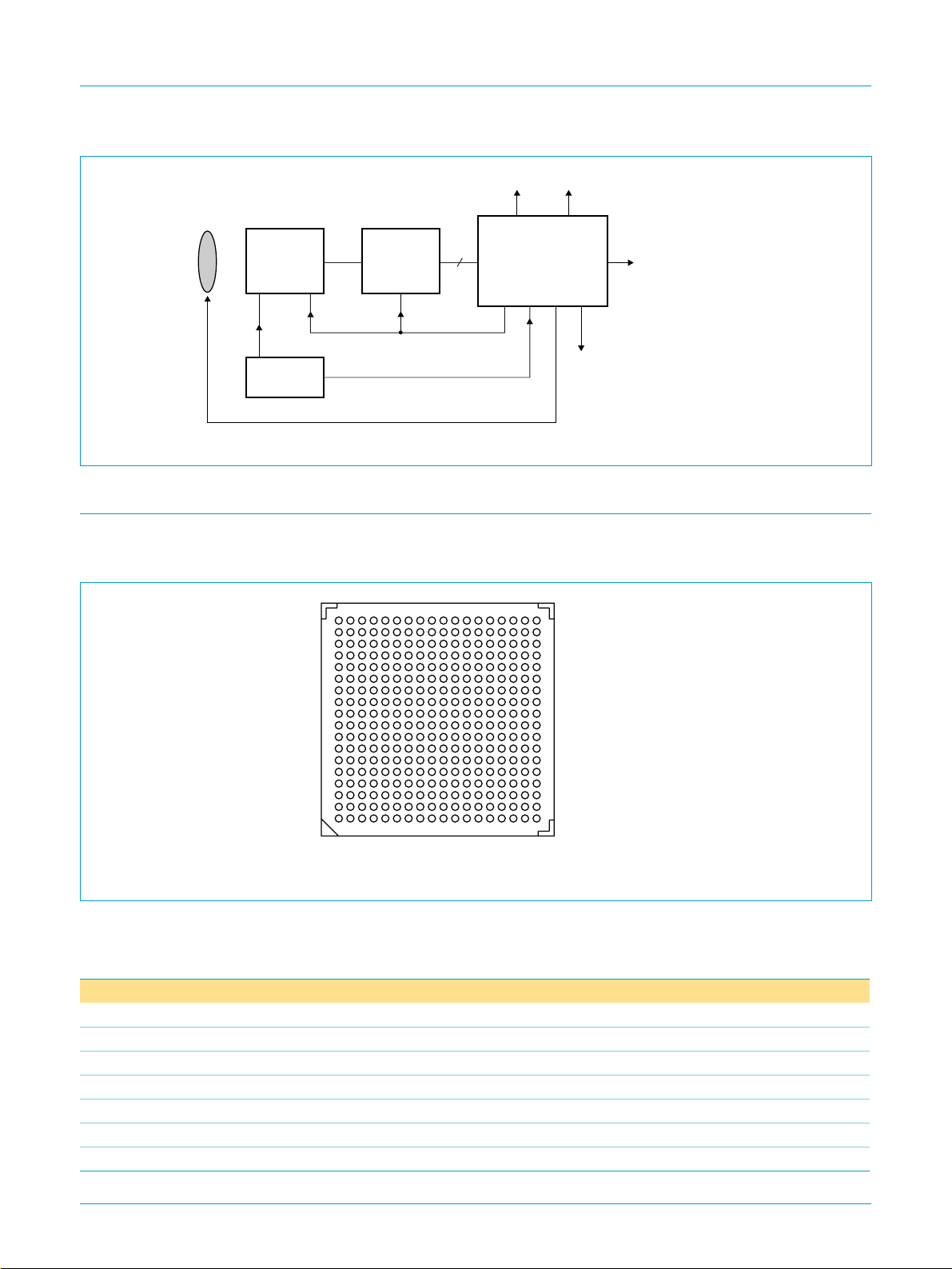
6. Pinning information
6.1 Pinning
handbook, halfpage
V
U
T
R
P
N
M
L
K
J
H
G
F
E
D
C
B
A
to LCD to TV
TDA9952
2 4 6 8 1012141618
1 3 5 7 9 11 13 15 17
10
SAA8122A
to cards
(SSFDC, CF)
USB
IRDA
to PC
FCE687
SAA8122AEL
FCE677
Fig 3. Pin configuration (bottom view).
6.2 Pin description
Table 3: Pin description
Symbol Pin Type Description
V
DDD
V
SSA(DLL)
V
DDA(DLL)
DISP_VSYNC A4 O digital vertical synchronization signal
IO1/IRQ17 A5 I/O I/O port 0 bit 1 or interrupt request 17
V
DDA(LCDG)
V
DDA(OUTPUT2)
9397 750 07048
Objective specification Rev. 01 — 20 April 2000 5 of 26
A1 - digital supply voltage
A2 - analog ground for DLL of PPG
A3 - analog supply voltage for DLL of PPG
A6 P analog supply voltage for DAC component G
A7 P analog supply voltage for DAC video output 2
© Philips Electronics N.V. 2000. All rights reserved.

Philips Semiconductors
SAA8122A
Digital Still Camera Processor (ImagIC family)
Table 3: Pin description
…continued
Symbol Pin Type Description
CREF_BG1 A8 - band-gap 1
V
SS(BG)
A9 P ground for BG of video DAC
SYSRSTIN A10 I system reset input/output; active LOW
V
SS(RTC)
A11 P ground for RTC
T0_CAP0 A12 I timer 0 capture input 0
CNT2 A13 I timer 2 count pulse input
CNT1 A14 I timer 1 count pulse input
PWM0 A15 O timer 0 PWM output
ADC0 A16 I analog input signal 0 for level measurement
ADC3 A17 I analog input signal 3 for level measurement
V
SS(ADC)
A18 P ground for ADC
ANPPG1 B1 O PPG analog signal 1
IO6/IRQ22 B4 I/O I/O port 0 bit 6 or interrupt request 22
IO3/IRQ19 B5 I/O I/O port 0 bit 3 or interrupt request 19
LCD_G B6 O analog green signal
VIDEO_OUT2 B7 O video output signal 2
V
SSA(ref)
B8 O analog reference ground
SC_TCK B9 I test clock input for surround scan chains
TCK B10 I test clock input
XTALCCDIN B11 - oscillator input from a specific CCD crystal
V
DDA(SPLL)
V
SS(PLL)
B12 P analog supply voltage for SPLL
B13 P ground for PLL
CNT0 B14 I timer 0 count pulse input
V
SSA(ref)(ADC)
B15 O analog reference ground for ADC
ADC2 B16 I analog input signal 2 for level measurement
V
DDA(ADC)
B17 P analog supply voltage for ADC
IO23 B18 I/O I/O port 2 bit 7
V
DDA(PPG1)
V
DDA(PPG0)
V
DDA(DLL)
C1 P analog supply voltage for PPG
C2 P analog supply voltage for PPG
C3 P analog supply voltage for DLL of PPG
IO7/IRQ23 C4 I/O I/O port 0 bit 7 or interrupt request 23
IO4/IRQ20 C5 I/O I/O port 0 bit 4 or interrupt request 20
LCD_R C6 O analog red signal
LCD_B C7 O analog blue signal
V
DDA(OUTPUT1)
V
DDA(BG)
C8 P analog supply voltage for DAC video output 1
C9 P analog supply voltage for BG of video DAC
TMS C10 I test mode select input
XTAL32KIN C11 - oscillator input from a 32 kHz crystal
XTAL10IN C12 - oscillator input from a 10 MHz crystal
GATE2 C13 I timer 2 gate input
V
DDA(PLL)
C14 P analog supply voltage for PLL
9397 750 07048
Objective specification Rev. 01 — 20 April 2000 6 of 26
© Philips Electronics N.V. 2000. All rights reserved.

Philips Semiconductors
SAA8122A
Digital Still Camera Processor (ImagIC family)
Table 3: Pin description
…continued
Symbol Pin Type Description
PWM1 C15 O timer 1 PWM output
ADC1 C16 I analog input signal 1 for level measurement
IO22 C17 I/O I/O port 2 bit 6
IO16 C18 I/O I/O port 2 bit 0
ANPPG7 D1 O PPG analog signal 7
V
SSA(PPG1)
D2 P analog ground for PPG
DISP_HSYNC D3 O digital horizontal synchronization signal
IO5/IRQ21 D4 I/O I/O port 0 bit 5 or interrupt request 21
IO0/IRQ16 D5 I/O I/O port 0 bit 0 or interrupt request 16
V
SSA(LCD)
V
SS(OUTPUT)
D6 P analog ground for display RGB
D7 P ground for DAC video output
CREF_BG2 D8 - band-gap 2
TDO D9 O test data output
TDI D10 I test data input
XTAL32KOUT D11 - oscillator output from a 32 kHz crystal
XTAL10OUT D12 - oscillator output from a 10 MHz crystal
T0_CAP1 D13 I timer 0 capture input 1
GATE0 D14 I timer 0 gate input
PWM2 D15 O timer 2 PWM output
IO17 D16 I/O I/O port 2 bit 1
IO15 D17 I/O I/O port 1 bit 7
IO11 D18 I/O I/O port 1 bit 3
PPG1 E1 O PPG digital signal 0
PPG2 E2 O PPG digital signal 1
ANPPG8 E3 O PPG analog signal 8
V
DDA(PPG0)
E4 P analog supply voltage for PPG
IO2/IRQ18 E5 I/O I/O port 0 bit 2 or interrupt request 18
V
DDA(LCDR)
V
DDA(LCDB)
E6 P analog supply voltage for DAC component R
E7 P analog supply voltage for DAC component B
VIDEO_OUT1 E8 O video output signal 1
SYSRST E9 O system reset output; active LOW
TRST E10 I test reset input
V
DDD(RTC)
E11 P digital supply voltage for RTC
XTALCCDOUT E12 - oscillator output from a specific CCD crystal
GATE1 E14 I timer 1 gate input
IO18 E15 I/O I/O port 2 bit 2
IO10 E16 I/O I/O port 1 bit 2
IO9 E17 I/O I/O port 1 bit 1
UA_CLK E18 I UART external clock
PPG5 F1 O PPG digital signal 4
PPG6 F2 O PPG digital signal 5
9397 750 07048
Objective specification Rev. 01 — 20 April 2000 7 of 26
© Philips Electronics N.V. 2000. All rights reserved.

Philips Semiconductors
SAA8122A
Digital Still Camera Processor (ImagIC family)
Table 3: Pin description
…continued
Symbol Pin Type Description
PPG3 F3 O PPG digital signal 2
ANPPG5 F4 O PPG analog signal 5
ANPPG3 F5 O PPG analog signal 3
V
SS
V
SS
V
DD
V
DD
V
DD
V
DD
V
DD
F6 - ground
F7 - ground
F8 - supply voltage
F9 - supply voltage
F10 - supply voltage
F11 - supply voltage
F12 - supply voltage
IO20 F13 I/O I/O port 2 bit 4
IO19 F14 I/O I/O port 2 bit 3
IO12 F15 I/O I/O port 1 bit 4
CTS F16 I UART clear to send
RXD F17 I UART receive input
TXD F18 O UART transmit output
PPG10 G1 O PPG digital signal 17
PPG12 G2 O PPG digital control signal 1
PPG8 G3 O PPG digital signal 8
PPG4 G4 O PPG digital signal 3
ANPPG6 G5 O PPG analog signal 6
ANPPG2 G6 O PPG analog signal 2
V
DD
V
SS
V
SS
V
SS
V
SS
V
DD
G7 - supply voltage
G8 - ground
G9 - ground
G10 - ground
G11 - ground
G12 - supply voltage
IO21 G13 I/O I/O port 2 bit 5
IO13 G14 I/O I/O port 1 bit 5
RTS G15 O UART request to send
2
SDA G16 I/O I
SCL G17 I/O I
C-bus data
2
C-bus clock
n.c. G18 - not connected
HDHREF H1 I/O PPG horizontal synchronization signal
VDVS H2 I/O PPG vertical synchronization signal
PPG13 H3 O PPG digital control signal 2
PPG7 H4 O PPG digital control signal 6
PPG14 H5 O PPG digital control signal 3
ANPPG4 H6 O PPG analog signal 4
V
DD
H7 - supply voltage
9397 750 07048
Objective specification Rev. 01 — 20 April 2000 8 of 26
© Philips Electronics N.V. 2000. All rights reserved.
 Loading...