

Philips SAA8117HL-C1-R5, SAA8117HL-C2 Datasheet
DATA SH EET
Product specification
File under Integrated Circuits, IC22
1999 Apr 02
INTEGRATED CIRCUITS
SAA8117HL
Digital camera USB interface IC

1999 Apr 02 2
Philips Semiconductors Product specification
Digital camera USB interface IC SAA8117HL
CONTENTS
1 FEATURES
2 APPLICATIONS
3 GENERAL DESCRIPTION
4 ORDERING INFORMATION
5 QUICK REFERENCE DATA
6 BLOCK DIAGRAM
7 PINNING
8 FUNCTIONAL DESCRIPTION
8.1 Video synchronization
8.2 CIF formatter
8.3 Compression engine
8.4 Transfer buffer
8.5 SNERT interface
8.6 Sensor pulse generator
8.7 Pulse diagrams
8.8 USB video FIFO
8.9 PSIE-MMU, I2C-bus interface and USB RAM
space
8.10 ATX and external ATX interface
8.11 Audio
8.12 Power management
9 CONTROL REGISTER DESCRIPTION
9.1 SNERT (UART)
9.2 I2C-bus interface
9.2.1 Commands
9.2.2 End-points
9.2.3 Control top registers
9.2.4 Video FIFO registers
9.2.5 ADIF top registers
10 LIMITING VALUES
11 THERMAL CHARACTERISTICS
12 CHARACTERISTICS
13 TIMING
14 APPLICATION INFORMATION
15 PACKAGE OUTLINE
16 SOLDERING
16.1 Introduction to soldering surface mount
packages
16.2 Reflow soldering
16.3 Wave soldering
16.4 Manual soldering
16.5 Suitability of surface mount IC packages for
wave and reflow soldering methods
17 DEFINITIONS
18 LIFE SUPPORT APPLICATIONS
19 PURCHASE OF PHILIPS I2C COMPONENTS

1999 Apr 02 3
Philips Semiconductors Product specification
Digital camera USB interface IC SAA8117HL
1 FEATURES
• Medium resolution CCD sensors (PAL non-interlaced
mode) or VGA CCD sensors (progressive mode)
• D1 digital video input (8 bits YUV 4 : 2 : 2,
time multiplexed)
• Internal Pulse Pattern Generator (PPG) dedicated for
medium resolution Sharp or compatible sensors and
VGA sensors and for frame rate selection
• Video formatter (programmable CIF formatter and
compression engine) controlled via SNERT (UART)
interface
• Selectable output frame rate (1 fps in VGA, up to 15 fps
in CIF format)
• Video packetizer FIFO
• I
2
C-bus interface for communication between the USB
protocol hardware and the external microcontroller
• Integrated analog bus driver (ATX)
• Microphone/audio input to USB (FGA, ADC, PLL and
decimator filter)
• Integrated analog bus driver (ATX)
• Integrated main oscillator
• Miscellaneous functions e.g. power management,
PLL backup oscillator.
2 APPLICATIONS
• Low-cost desktop video applications with USB interface.
3 GENERAL DESCRIPTION
The SAA8117HL is a monolithic integrated circuit which
can be used in PC video cameras to convert D1 video
signals and analog audio signals to properly formatted
USB packets.
It is designed as a back-end for the SAA8110G or
SAA8112HL (general camera digital processing ICs) and
is optimized for use with the TDA8784/87 (camera
pre-processing IC) and the 83C51RC (microcontroller).
4 ORDERING INFORMATION
TYPE
NUMBER
PACKAGE
NAME DESCRIPTION VERSION
SAA8117HL LQFP100 plastic low profile quad flat package; 100 leads; body 14 × 14 × 1.4 mm SOT407-1

1999 Apr 02 4
Philips Semiconductors Product specification
Digital camera USB interface IC SAA8117HL
5 QUICK REFERENCE DATA
Measured over full voltage and operating temperature range.
SYMBOL PARAMETER CONDITIONS MIN. TYP. MAX. UNIT
V
DDD
digital supply voltage 3.0 3.3 3.6 V
V
DDA
analog supply voltage 3.0 3.3 3.6 V
I
DD(tot)
total supply current VDD= 3.3 V − 91 − mA
V
i(bus)
input voltage on I2C-bus interface pins 5 V tolerant TTL compatible V
V
o(bus)
output voltage on I2C-bus interface pin SDA 5 V tolerant TTL compatible V
V
i(n)
input signal voltage on other pins 3.0V<VDD< 3.6 V low voltage TTL compatible V
V
o(n)
output signal voltage on other pins 3.0V<VDD< 3.6 V low voltage TTL compatible V
f
clk
clock frequency − 48 − MHz
P
tot
total power dissipation T
amb
=25°C − 300 − mW
T
stg
storage temperature −55 − +150 °C
T
amb
operating ambient temperature 0 25 70 °C
T
j
junction temperature T
amb
=70°C −40 − +125 °C
1999 Apr 02 5
Philips Semiconductors Product specification
Digital camera USB interface IC SAA8117HL
This text is here in white to force landscape pages to be rotated correctly when browsing through the pdf in the Acrobat reader.This text is here in
_white to force landscape pages to be rotated correctly when browsing through the pdf in the Acrobat reader.This text is here inThis text is here in
white to force landscape pages to be rotated correctly when browsing through the pdf in the Acrobat reader. white to force landscape pages to be ...
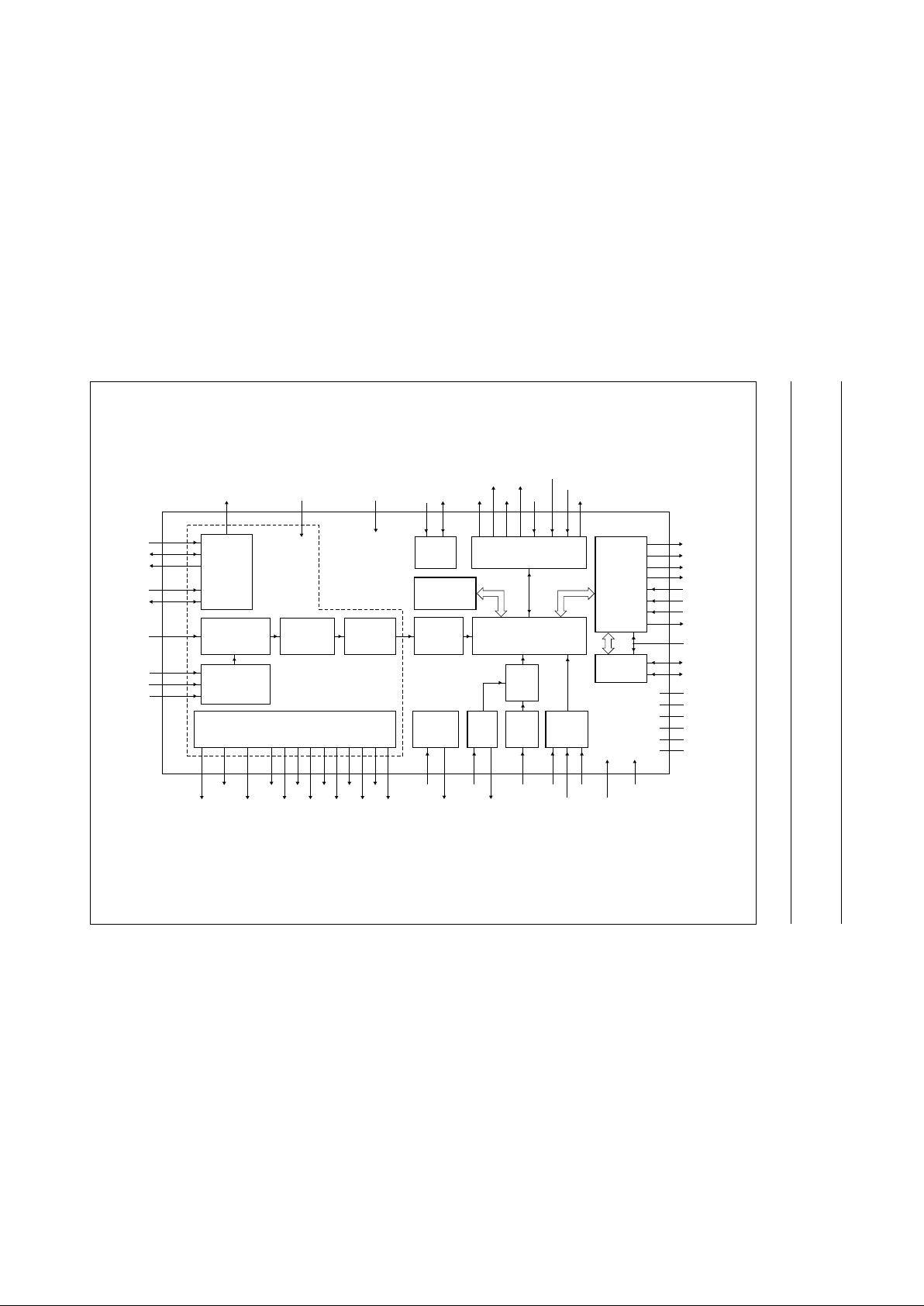
6 BLOCK DIAGRAM
FCE130
SAA8117HL
n
dbook, full pagewidth
CIF
FORMATTER
SNERT
INTERFACE
AND HATCH
ATX
EXTERNAL
ATX
INTERFACE
COMPRESSION
ENGINE
TRANSFER
BUFFER
MAIN
OSCILLATOR
AUDIO
PLL
VIDEO
SYNCHRONISATION
PATTERN PULSE GENERATOR
(PPG)
50
49
47
VSYNC
HREF
35, 36,
37, 38,
42, 43
44, 45
YUV0
to
YUV7
LLC
55
56
58
57
SNDA
SNCL
SNRES
SMP
51
RESET
76
GENPOR
I2C-BUS
INTERFACE
I
2
S-BUS
INTERFACE
USB
RAM SPACE
POWER
MANAGEMENT
USB
VIDEO
FIFO
PSIE
MMU
95
SDA
98
DCDCON
96
CLOCKON
77
UCPOR
64
UCINT
93
CLOCK
94
SCL
97100
TRC
SNAPSHOT
99
SUSREADYNOT
65 87
XOUT2
86
XIN2
AUDIO
AMP
79
AUDIO
ADC
MIC
90
DA
3, 2, 1
M0 to M2
81, 82, 83
REF1 to REF3
89WS91
BCK
XOUT1
XIN1
53
52
RESERVED2
RESERVED1
65
63
66
SUSPEND
SPEED
VM
67
VP
73
OEBAR
68
71
RCV
VMO
72
VPO
60
61
32, 25, 15
85, 84, 62, 7
70, 48, 41, 39
54, 34, 26, 14
88, 80, 78, 59, 4
92, 75, 69, 46, 40
ATXDP
74
ATXCTRL
ATXDM
V
DD1
to V
DD3
V
DDA1
to V
DDA4
V
DDD1
to V
DDD4
GND1 to GND4
AGND1 to AGND5
DGND1 to DGND5
19, 18
17, 16
A1 to A4
13, 12
11, 10
23, 22,
21
B1 to B4
C1 to C3
24
RG
20
SHUTTER
28
SHP
29
SHD
27
CLK1
33
CLK2
8
CLPDM
9
CLPOB30VD
31
HD
Fig.1 Block diagram.

1999 Apr 02 6
Philips Semiconductors Product specification
Digital camera USB interface IC SAA8117HL
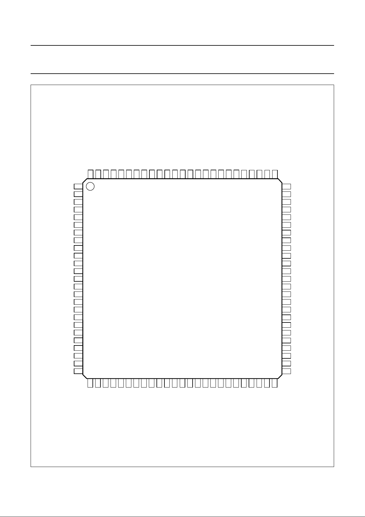
7 PINNING
SYMBOL PIN TYPE DESCRIPTION
M2 1 I test mode control signal bit 2
M1 2 I test mode control signal bit 1
M0 3 I test mode control signal bit 0
AGND1 4 P analog ground 1 for main oscillator (48 MHz, 3rd overtone)
XIN1 5 I oscillator input
XOUT1 6 O oscillator output
V
DDA1
7 P analog supply voltage 1 for main oscillator (48 MHz, 3rd overtone)
CLPDM 8 O dummy clamp pulse output to TDA8784/87
CLPOB 9 O optical black clamp pulse output to TDA8784/87
B4 10 O vertical CCD load pulse output (VH1X)
B3 11 O vertical CCD load pulse output (VH3X)
B2 12 O vertical CCD load pulse output
B1 13 O vertical CCD load pulse output
GND1 14 P ground 1 for output buffers
V
DD1
15 P supply voltage 1 for output buffers
A4 16 O vertical CCD transfer pulse output (V4X)
A3 17 O vertical CCD transfer pulse output (V3X)
A2 18 O vertical CCD transfer pulse output (V2X)
A1 19 O vertical CCD transfer pulse output (V1X)
SHUTTER 20 O shutter control output for CCD charge reset
C3 21 O horizontal CCD transfer pulse output
C2 22 O horizontal CCD transfer pulse output (FH1)
C1 23 O horizontal CCD transfer pulse output (FH2)
RG 24 O reset output for CCD output amplifier gate
V
DD2
25 P supply voltage 2 for output buffers
GND2 26 P ground 2 for output buffers
CLK1 27 O pixel clock output to TDA8784/87and SAA8110G
SHP 28 O preset sample-and-hold pulse output to TDA8784/87 (FCDS)
SHD 29 O data sample-and-hold pulse output to TDA8784/87 (FS)
VD 30 O vertical definition pulse output to SAA8110G
HD 31 O horizontal definition pulse output to SAA8110G
V
DD3
32 P supply voltage 3 for output buffers
CLK2 33 O double pixel clock output to SAA8110G
GND3 34 P ground 3 for output buffers
YUV0 35 I multiplexed input YUV-bit 0 (LSB)
YUV1 36 I multiplexed input YUV-bit 1 input
YUV2 37 I multiplexed input YUV-bit 2 input
YUV3 38 I multiplexed input YUV-bit 3 input
V
DDD1
39 P digital supply voltage 1 for input buffers and predrivers and one part of the digital
core

1999 Apr 02 7
Philips Semiconductors Product specification
Digital camera USB interface IC SAA8117HL
DGND1 40 P digital ground 1 for input buffers and predrivers and for the digital core
V
DDD2
41 P digital supply voltage 2 for digital core
YUV4 42 I multiplexed input YUV-bit 4
YUV5 43 I multiplexed input YUV-bit 5
YUV6 44 I multiplexed input YUV-bit 6
YUV7 45 I multiplexed input YUV-bit 7
DGND2 46 P digital ground 2 for input buffers and predrivers and for the digital core
LLC 47 I line-locked clock input (delayed CLK2) for YUV-port from SAA8110G
V
DDD3
48 P digital supply voltage 3 for digital core
HREF 49 I horizontal reference input for YUV-port from SAA8110G
VSYNC 50 I vertical synchronization input for YUV-port from SAA8110G
RESET 51 I Power-on reset input (for video processing and PPG)
RESERVED1 52 − test pin (should not be used)
RESERVED2 53 − test pin (should not be used)
GND4 54 P ground 4 for output buffer
SNDA 55 I/O data I/O for SNERT-interface (communication between SAA8117HL and
SAA8110G)
SNCL 56 I input clock for SNERT-interface (communication between SAA8117HL and
SAA8110G)
SNRES 57 O output reset for SNERT-interface (communication between SAA8117HL and
SAA8110G)
SMP 58 O output switch mode pulse for DC-to-DC power supply
AGND2 59 P analog ground 2 for ATX (transceiver)
ATXDP 60 I/O positive driver of the differential data pair input/output (ATX)
ATXDM 61 I/O negative driver of the differently data pair input/output (ATX)
V
DDA2
62 P analog supply voltage 2 for ATX
SPEED 63 O required output for ATX-backup solution
UCINT 64 O interrupt output from USB protocol hardware to microcontroller
SUSPEND 65 O control output from USB protocol hardware to microcontroller
VM 66 O required output for ATX-backup solution (txdn)
VP 67 O required output for ATX-backup solution (txdp)
RCV 68 I required output for ATX-backup solution
DGND3 69 P digital ground 3 for input buffers and predrivers and for the digital core
V
DDD4
70 P digital supply voltage 4 for one part of input buffers and predrivers and for the
digital core
VMO 71 I required input or ATX-backup solution (rxdn)
VPO 72 I required input for ATX-backup solution (rxdp)
OEBAR 73 O required output for ATX-backup solution
ATXCTRL 74 I required input for ATX-backup solution
DGND4 75 P digital ground 4 for input buffers and predrivers and for the digital core
GENPOR 76 I Power-on reset input (for USB protocol hardware)
SYMBOL PIN TYPE DESCRIPTION

1999 Apr 02 8
Philips Semiconductors Product specification
Digital camera USB interface IC SAA8117HL
UCPOR 77 O output control from USB protocol hardware to microcontroller
AGND3 78 P analog ground 3 for FGA
MIC 79 I microphone input
AGND4 80 P analog ground 4 for FGA/ADC
REF1 81 I reference input voltage 1 for FGA/ADC (double-bonding)
REF2 82 I reference input voltage 2 for DACn (used in the ADC)
REF3 83 I reference input voltage 3 for DACp (used in the ADC)
V
DDA3
84 P analog supply voltage 3 for FGA/ADC
V
DDA4
85 P analog supply voltage 4 for PLL
XIN2 86 I oscillator input required for PLL backup solution
XOUT2 87 O oscillator output required for PLL backup solution
AGND5 88 P analog ground 5 for PLL
WS 89 I I
2
S-bus word select (required for FGA/ADC backup solution)
DA 90 I I
2
S-bus data (required for FGA/ADC backup solution)
BCK 91 I I
2
S-bus clock (required for FGA/ADC backup solution)
DGND5 92 P digital ground 5 for input buffers and predrivers and for the digital core
CLOCK 93 O clock output from USB protocol hardware to microcontroller
SCL 94 I slave I
2
C-bus clock input
SDA 95 I/O slave I
2
C-bus data input/output
CLOCKON 96 O control output for main oscillator switched on
SNAPSHOT 97 I input for remote wake-up (snapshot)
DCDCON 98 O control output from USB protocol hardware to power supply module
SUSREADYNOT 99 I input from microcontroller for SUSPEND mode
TRC 100 I threshold control input for enabling the clock (switching for power management)
SYMBOL PIN TYPE DESCRIPTION
1999 Apr 02 9
Philips Semiconductors Product specification
Digital camera USB interface IC SAA8117HL
Fig.2 Pin configuration.
handbook, full pagewidth
75
74
73
72
71
70
69
68
67
66
65
64
63
62
61
60
59
58
57
56
55
54
53
52
51
8079787776
MIC
AGND3
AGND4
V
DDA3
V
DDD4
REF1
REF2
REF3
UCPOR
GENPOR
ATXCTRL
OEBAR
VPO
VMO
DGND3
DGND4
V
DDD4
RCV
VP
VM
SUSPEND
UCINT
SPEED
V
DDA2
ATXDM
ATXDP
AGND2
SMP
SNRES
SNCL
SNDA
GND4
RESERVED2
RESERVED1
RESET
FCE131
M2
M1
M0
AGND1
XIN1
XOUT1
V
DDA1
CLPDM
CLPOB
B4
B3
B2
B1
GND1
V
DD1
V
DD2
GND2
V
DD3
V
DDD1
DGND1
DGND2
V
DDD2
V
DDD3
GND3
A4
A3
A2
A1
SHUTTER
C3
C2
C1
RG
TRC
SUSREADYNOT
DCDCON
SNAPSHOT
CLOCKON
SDA
SCL
CLOCK
DGND5
BCKDAWS
AGND5
XOUT2
XIN2
HD
CLK2
YUV0
YUV1
YUV2
YUV3
YUV4
YUV5
YUV6
YUV7
LLC
HREF
VSYNC
CLK1
SHP
SHD
VD
30
29
28
27
26
25
24
23
22
21
20
19
18
17
16
15
14
13
12
11
10
9
8
7
6
5
4
3
2
1
100
99989796959493929190898887868584838281
31323334353637383940414243444546474849
50
SAA8117HL
1999 Apr 02 10
Philips Semiconductors Product specification
Digital camera USB interface IC SAA8117HL
8 FUNCTIONAL DESCRIPTION
8.1 Video synchronization
The video synchronization module (see Fig.1) is capable
of locking onto the video signal thereby implementing a
horizontal gate signal HREF (HREF = HIGH when data is
valid) and a VS signal indicating the start of a new video
frame. This module expects, in the PAL mode, 288 active
lines from a total of 292 lines and in the VGA mode,
480 active lines from a total of 486 lines. The module
generates control signals for the CIF formatter.
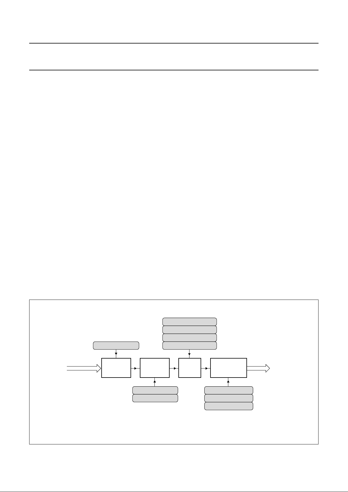
8.2 CIF formatter
The video data must be progressive (or non-interlaced)
and in 4 :2:2(UYVY) format. The CIF formatter module
(see Figs 1 and 3) is programmable to perform down
scaling from 512 × 288 (PAL mode) or 640 × 480 (VGA
mode) to 352 × 288 or 176 × 144 without affecting the
aspect ratio.
The horizontal scaling is achieved with a Variable Phase
Delay filter (VPD-4). To avoid aliasing, this module also
contains a prefilter which has three modes:
• Prefilter A (3 taps)
• Prefilter B (7 taps)
• Prefilter B-comb (13 taps).
Prefilter B-comb is similar to prefilter B, but inserts extra
taps with amplification 0.
This prefilter must be chosen by selecting prefilter B and
setting SN_Prefilter_B_Comb. Prefilter B-comb can be
used independently from prefilter A.
The incoming 4:2:2 data is vertically filtered to 4 : 2 : 0
by throwing away colour samples. In the even lines the
V-samples are discarded, in the odd lines the U-samples.
The vertical scaling in PAL mode is from CIF (352 × 288)
to QCIF (176 × 144) only. This is done via a vertical
prefilter A (3 taps). In VGA mode a VPD-4 vertical filter is
applied to scale from 640 × 480 to CIF and QCIF.
From the QCIF image a sub-QCIF cut (128 × 96) can be
made. Due to the granularity of the cropping origin, a
UV interchange can occur. This interchange can be
corrected with SN_EIRRAH.
In VGA mode the CIF formatter can be bypassed to create
a full resolution snapshot. The snapshot can be in 4 :2:0
and in 4 :2:2 format, selectable with SN_4 :2:2.
8.3 Compression engine
The compression engine module (see Figs 1 and 3) works
on CIF format only. The CIF data is compressed to a fixed
number of bytes per frame. This number can be selected
leading a compression factor of either 3 or 4. As a result
the data stream of CIF4:2:0 equals the data stream of
QCIF 4:2:2 (3times compression) or QCIF 4:2:0
(4 times compression). The algorithm is Philips
proprietary. Real-time decoding can be done in software
on any Pentium platform.
Fig.3 The CIF formatter and compression engine.
handbook, full pagewidth
FCE132
PREFILTER
A
PREFILTER
B
DOWN
SCALER
YUV0 to YUV7
to
transfer
buffer
COMPRESSION
ENGINE
SN_Output_Format_Select
SN_PAL_VGA
SN_EIRRAH
SN_4:2:2
SN_Prefilter A_On/Off
SN_Prefilter B_On/Off
SN_Prefilter B_Comb
SN_Compress
SN_Clk_Compress_On
SN_Compression_Ratio

1999 Apr 02 11
Philips Semiconductors Product specification
Digital camera USB interface IC SAA8117HL
8.4 Transfer buffer
The transfer buffer module (see Fig.1) ensures a smooth
transfer of the data to the FIFO of the USB. Moreover the
transfer buffer can insert in band synchronization words in
the video data stream.
This function can be switched on and off with
SN_In band_Control in register CONTROL17_0.
The synchronization words can only be used with
non-compressed data streams and are formatted like
0x00 0xFF 0x<framecounter>7<linecounter>9.
The subscript denotes the number of bits and the frame
counter is circular incrementing.
The non-compressed data is formatted like:
4:2:0:<optional sync word><Y0><Y1><Y2><Y3>
<C0><C2><Y4><Y5><Y6><Y7><C4><C6>....,
4:2:2: <optional sync word><Y0><Y1><Y2><Y3>
<U0><V0><U2><V2><Y4>....,
where C denotes U-data in the even lines (0, 2, 4, etc.)
and V-data in the odd lines (1, 3, 5, etc.).
8.5 SNERT interface
In a USB camera the SAA8110G will operate on a clock
frequency which depends on the actual frame rate. For the
slowest frame rates, this frequency can be so low that the
SNERT communication is no longer functional over the
specified entire frequency range of the microcontroller.
The microcontroller must adapt its SNERT bus frequency
to a frequency appropriate for the current mode in which
the SAA8110G is operating.
The SAA8117HL itself is also partly controlled via SNERT.
The CIF formatter, compression engine and the PPG
function are controlled via SNERT. This SNERT interface
works independently from the frame rate and can always
be operated in the full frequency range.
8.6 Sensor pulse generator
The SAA8117HL incorporates a Pulse Pattern Generator
(PPG) function. The PPG can be used for PAL medium
resolution Sharp sensors (LZ2423) or compatible CCD
sensors. The SAA8117HL can also handle VGA type CCD
sensors, so a set of pulses is provided to simplify the use
of such sensors. Depending on the type of sensor, it will be
necessary to reformat these pulses externally according to
the sensor specification.
It should be noted that in case of medium resolution Sharp
or compatible sensors an external inverter driver is
required to convert the 3 V pulses into a voltage suitable
for the used CCD sensor. For the medium resolution Sharp
CCD sensor driver, the name of the pins to which the PPG
pulses must be connected are indicated between brackets
in the SAA8117HL pinning list (pins C3, B1 and B2 are not
used).
For both type of sensors the PPG generates 8 different
frame rates (see Table 6). The active video size is
512 × 288 for PAL and 640 × 480 for VGA. The total H × V
size is 685 × 292 for PAL and 823 × 486 for VGA.
It should be noted that additional HD pulses are added
during the vertical blanking interval to reach a total of
312 lines in PAL mode and 525 lines in VGA mode as
required by the SAA8110G.
The following registers are associated with the PPG:
• CONTROL17_0
• CONTROL17_2
• PPG_SHUTTERSPEED_0
• PPG_SHUTTERSPEED_1
• PPG_CLPOB_START_LSB
• PPG_CLPOB_STOP_LSB
• PPG_CLPDM_START_LSB
• PPG_CLPDM_STOP_LSB
• CLPMSB.
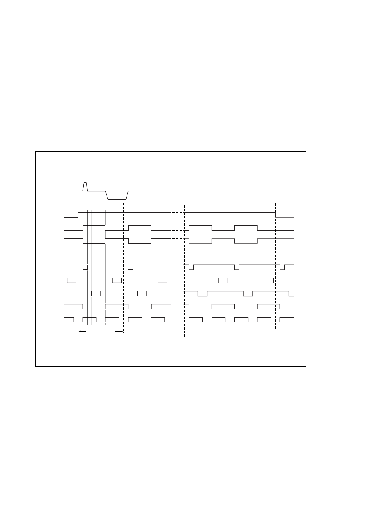
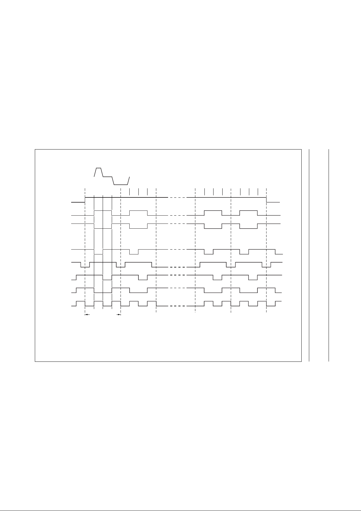
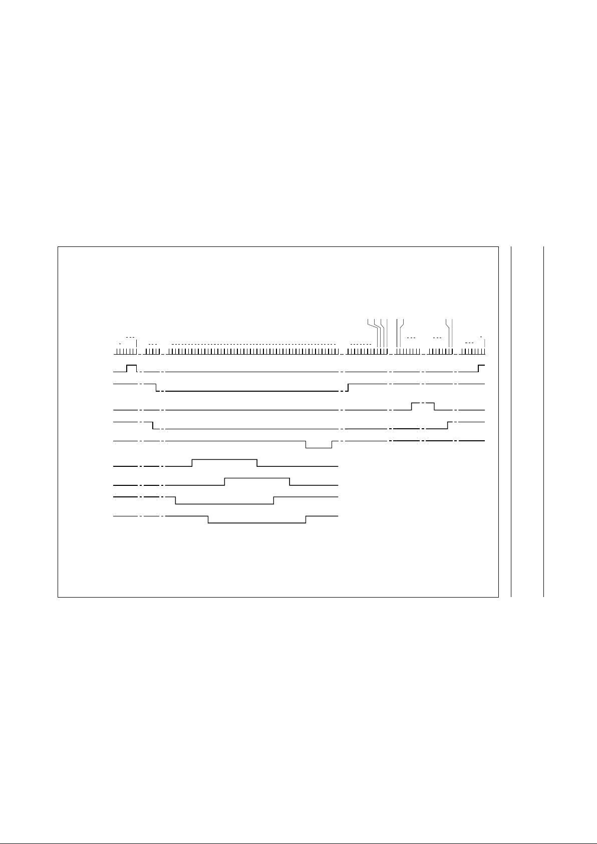
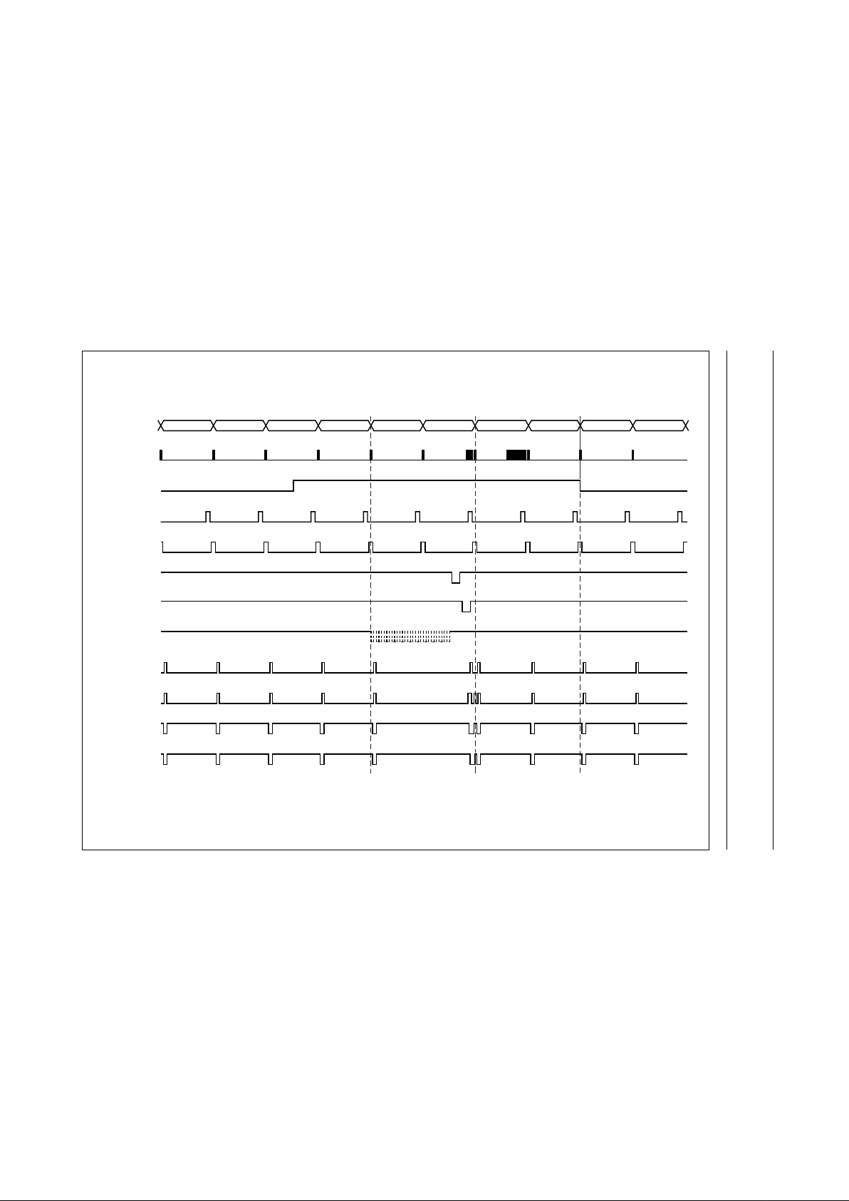
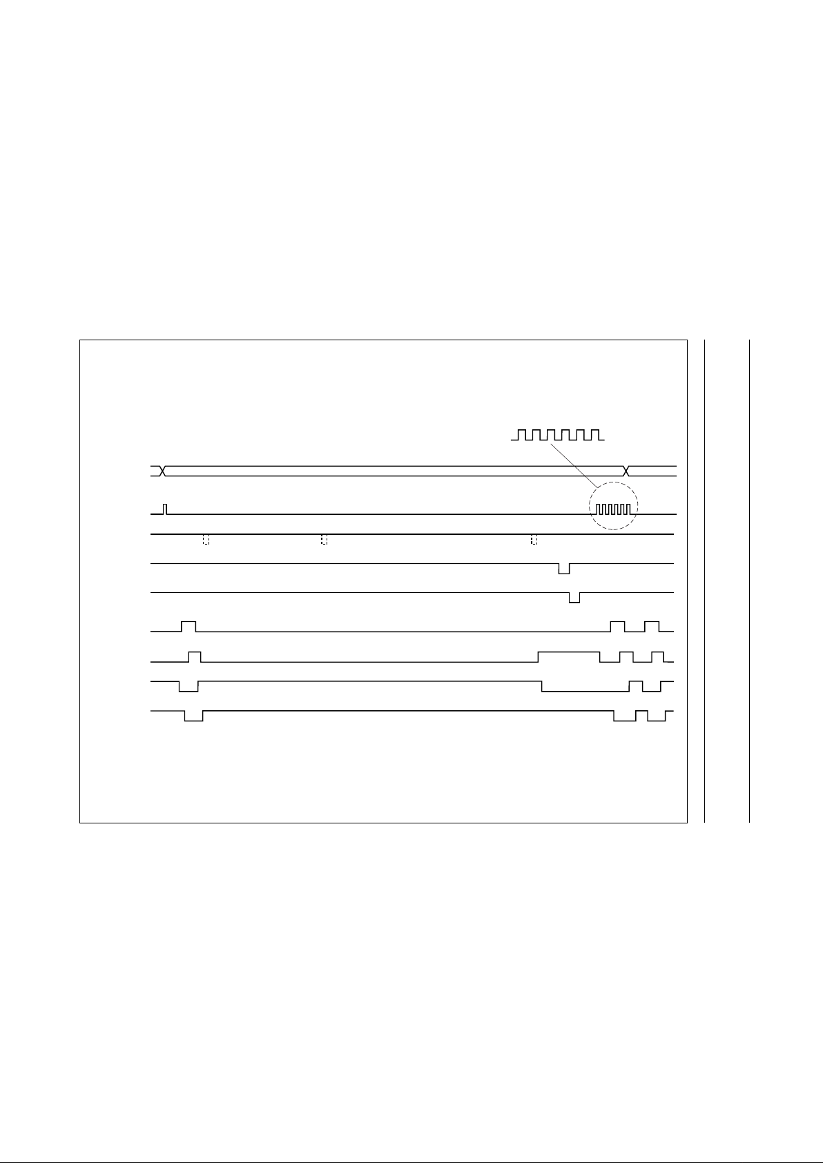
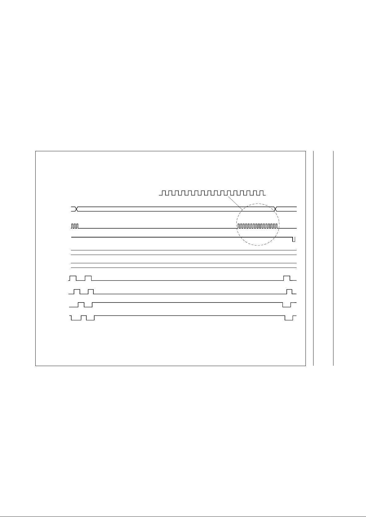
8.7 Pulse diagrams
For medium resolution CCD sensors (PAL):
• High-speed pulses, see Figs 4 and 5
• Horizontal pulses, see Fig.6
• Vertical pulses, see Figs 7 to 11.
For VGA-sensors:
• High-speed pulses, see Figs 12 to 14
• Horizontal pulses, see Fig.15
• Vertical pulses, see Figs 16 to 21.
1999 Apr 02 12
Philips Semiconductors Product specification
Digital camera USB interface IC SAA8117HL
This text is here in white to force landscape pages to be rotated correctly when browsing through the pdf in the Acrobat reader.This text is here in
_white to force landscape pages to be rotated correctly when browsing through the pdf in the Acrobat reader.This text is here inThis text is here in
white to force landscape pages to be rotated correctly when browsing through the pdf in the Acrobat reader. white to force landscape pages to be ...
handbook, full pagewidth
CLOCK ENABLE
CCD OUTPUT
C1 (FH1)
C2 (FH2)
FCE133
RG (FR)
SHD (FS)
SHP(FCDS)
CLK1
CLK2
02461357802491356879 900 2461357802491356879
mode 0: 1/(4.8 MHz)
Fig.4 High-speed pulses for PAL medium resolution (1).
1999 Apr 02 13
Philips Semiconductors Product specification
Digital camera USB interface IC SAA8117HL
This text is here in white to force landscape pages to be rotated correctly when browsing through the pdf in the Acrobat reader.This text is here in
_white to force landscape pages to be rotated correctly when browsing through the pdf in the Acrobat reader.This text is here inThis text is here in
white to force landscape pages to be rotated correctly when browsing through the pdf in the Acrobat reader. white to force landscape pages to be ...
handbook, full pagewidth
CLOCK ENABLE
CCD OUTPUT
C1 (FH1)
C2 (FH2)
FCE134
RG (FR)
SHD (FS)
SHP (FCDS)
CLK1
CLK2
012301230 301230123
mode 1: 1/(4 MHz)
mode 2: 1/(3 MHz)
mode 3: 1/(2.4 MHz)
mode 4: 1/(2 MHz)
mode 5: 1/(1.5 MHz)
mode 6: 1/(1 MHz)
mode 7: 1/(750 kHz)
Fig.5 High-speed pulses for PAL medium resolution (2).
1999 Apr 02 14
Philips Semiconductors Product specification
Digital camera USB interface IC SAA8117HL
This text is here in white to force landscape pages to be rotated correctly when browsing through the pdf in the Acrobat reader.This text is here in
_white to force landscape pages to be rotated correctly when browsing through the pdf in the Acrobat reader.This text is here inThis text is here in
white to force landscape pages to be rotated correctly when browsing through the pdf in the Acrobat reader. white to force landscape pages to be ...
FCE135
handbook, full pagewidth
HD
14 0
CLPOB
(1) (1)
(1)
CLOCK ENABLE
15
91
SHUTTER (OFDX)
64 72
A1 (V1X)
29 49
A2 (V2X)
39 59
A3 (V3X)
24
54
A4 (V4X)
34 64
CLPDM
(1)
683
685/0
4
12
16
74
612 A511
613 A512
614 BLK
619 BLK
636 BLK
641 BLK
642
643
680
685/0
2
91
99
100 BLK
101 BLK
102 A1
103 A2
22
Fig.6 Horizontal pulses for PAL medium resolution.
(1) CLPOB and CLPDM are programmable.
1999 Apr 02 15
Philips Semiconductors Product specification
Digital camera USB interface IC SAA8117HL
This text is here in white to force landscape pages to be rotated correctly when browsing through the pdf in the Acrobat reader.This text is here in
_white to force landscape pages to be rotated correctly when browsing through the pdf in the Acrobat reader.This text is here inThis text is here in
white to force landscape pages to be rotated correctly when browsing through the pdf in the Acrobat reader. white to force landscape pages to be ...
FCE136
handbook, full pagewidth
INE#
HD
VD
CLPOB (DCP)
CLPDM (BCP)
B4 (VH1X)
289
A285
290
A286
291
A287
292
A288
1
Hd
2
Hd
3
AL1
4
AL2
5
A1
6
A2
A1 (V1X)
A3 (V3X)
A4 (V4X)
A2 (V2X)
B3 (VH3X)
SHUTTER (OFDX)
Fig.7 Vertical pulses for PAL medium resolution (1).

1999 Apr 02 16
Philips Semiconductors Product specification
Digital camera USB interface IC SAA8117HL
This text is here in white to force landscape pages to be rotated correctly when browsing through the pdf in the Acrobat reader.This text is here in
_white to force landscape pages to be rotated correctly when browsing through the pdf in the Acrobat reader.This text is here inThis text is here in
white to force landscape pages to be rotated correctly when browsing through the pdf in the Acrobat reader. white to force landscape pages to be ...
handbook, full pagewidth
INE#
HD
292 1 2
1
4
SHUTTER (OFDX)
1
4
A3 (V3X)
A4 (V4X)
B4 (VH1X)
B3 (VH3X)
A1 (V1X)
A2 (V2X)
29
49
64
72
29
49
39
59
39
59
24
54
24
54
34
64
34
64
FCE137
Fig.8 Vertical pulses for PAL medium resolution (2).
1999 Apr 02 17
Philips Semiconductors Product specification
Digital camera USB interface IC SAA8117HL
This text is here in white to force landscape pages to be rotated correctly when browsing through the pdf in the Acrobat reader.This text is here in
_white to force landscape pages to be rotated correctly when browsing through the pdf in the Acrobat reader.This text is here inThis text is here in
white to force landscape pages to be rotated correctly when browsing through the pdf in the Acrobat reader. white to force landscape pages to be ...
handbook, full pagewidth
INE#
HD
1
2 3
1
4
SHUTTER (OFDX)
1
4
545
553
A3 (V3X)
A4 (V4X)
B4 (VH1X)
584
599
B3 (VH3X)
A1 (V1X)
A2 (V2X)
29
49
64
72
599
614
664
6842949
674
9
39
59
39
59
554
644
4
24
54
24
54
559
14
34
64
34
64
669
FCE138
14683
679
675
671
667
663
659
655
651
647
RESET_DATA [9 to 0] + 8RESET_DATA [9 to 0]
Fig.9 Vertical pulses for PAL medium resolution (3).
1999 Apr 02 18
Philips Semiconductors Product specification
Digital camera USB interface IC SAA8117HL
This text is here in white to force landscape pages to be rotated correctly when browsing through the pdf in the Acrobat reader.This text is here in
_white to force landscape pages to be rotated correctly when browsing through the pdf in the Acrobat reader.This text is here inThis text is here in
white to force landscape pages to be rotated correctly when browsing through the pdf in the Acrobat reader. white to force landscape pages to be ...
handbook, full pagewidth
INE#
HD
2
3 4
1
4
SHUTTER (OFDX)
1
4
A3 (V3X)
A4 (V4X)
B4 (VH1X)
B3 (VH3X)
A1 (V1X)
A2 (V2X)
64
72
29
49
39
59
24
54
34
64
664
6842949
674939
59
42454
143464
669
FCE139
14683
679
675
671
667
663
659
655
651
647
643
639
635
631
627
623
619
615
611
607
603
599
595
591
587
583
579
575
571
567
Fig.10 Vertical pulses for PAL medium resolution (4).
 Loading...