

Philips SAA8116HL, SAA8116ET Datasheet

INTEGRATED CIRCUITS
DATA SH EET
SAA8116
DigitalPC-camerasignalprocessor
including microcontroller and USB
interface
Product specification
Supersedes data of 2000 Dec 6
File under Integrated Circuits, IC22
2001 May 04

Philips Semiconductors Product specification
Digital PC-camera signal processor including
microcontroller and USB interface
FEATURES
• Embedded microcontroller (80C51 core based) for
control loops Auto Optical Black (AOB), Auto White
Balance (AWB), AutoExposure (AE) and USB interface
control
• Compliant for VGA CCD and VGA CMOS sensors
(RGB Bayer)
• USB 1.1 compliant bus-powered USB device with
integrated power management and POR circuit
• RGB processing
• Optical black processing
• Defect pixel concealment
• Programmable colour matrix
• RGB to YUV transform
• Programmable gamma correction (including knee)
• Programmable edge enhancement
• Video formatter with SIF/QSIF downscaler
• Compression engine
• Flexible Measurement Engine (ME) with up to eight
measurements per frame
• Internal Pulse Pattern Generator (PPG) for wide range
of VGA CCDs (Sony, Sharp and Panasonic) and frame
rate selection
• ProgrammableH and V timing for thesupport of CMOS
sensors
• Programmable output pulse for switched mode power
supply of the sensor
• 3-wireinterface to control anexternal pre-processor IC,
such as the TDA8787A: Correlated Double
Sampling (CDS), Automatic Gain Control (AGC) and
10-bit ADC
• Analog microphone/audio input to USB: Low DropOut
(LDO) supply filter, microphone supply, low noise
amplifier, programmable amplifier, PLL and ADC
• Integrated analog USB driver (ATX)
• Integrated main oscillator, including a clock PLL, which
derives 48 MHzmain systemclock froma 12 or48 MHz
fundamental crystal.
APPLICATION
• USB PC-camera (video and audio).
GENERAL DESCRIPTION
The SAA8116 is a highly integrated third generation
USB PC-camera ICs. It is the successor to the
SAA8112HL and SAA8115HL. It processes the digitized
sensor data and converts it to a high quality, compressed
YUV signal. Together with the audio signal, this video
signal is then properly formatted in USB packets.
In addition, an 80C51 microcontroller derivative with five
I/O ports, I2C-bus, 512 bytes of RAM and 32 kbytes of
program memory is embedded in the SAA8116. The
microcontroller is used in combination with the
programmable statistical measurement capabilities to
provideadvanced AE, AWBand AOB.Themicrocontroller
is also used to control the USB interface.
SAA8116
ORDERING INFORMATION
TYPE
NUMBER
SAA8116HL LQFP100 plastic low profile quad flat package; 100 leads; body 14 × 14 × 1.4 mm SOT407-1
SAA8116ET TFBGA112 plastic thin fine-pitch ball grid array package; 112 balls; body 7 × 7 × 0.8 mm SOT630-1
2001 May 04 2
NAME DESCRIPTION VERSION
PACKAGE
Philips Semiconductors Product specification
Digital PC-camera signal processor including
SAA8116
microcontroller and USB interface
QUICK REFERENCE DATA
Measured over full voltage and temperature range: VDD= 3.3 V ±10% and T
SYMBOL PARAMETER CONDITIONS MIN. TYP. MAX. UNIT
V
DD
I
DD(tot)
V
i
V
o
f
(i)xtal
supply voltage 3.0 3.3 3.6 V
total supply current VDD= 3.3 V; T
=25°C (typ.) − 85
amb
input voltage 3.0V<VDD< 3.6 V low voltage TTL compatible V
output voltage 3.0V<VDD< 3.6 V low voltage TTL compatible V
crystal input frequency note 3 − 12 or 48 − MHz
δ crystal frequency duty factor − 50 − %
P
tot
T
stg
T
amb
T
j
total power dissipation; note 1 VDD= 3.3 V; T
=25°C (typ.) − 280 350 mW
amb
storage temperature −55 − +150 °C
ambient temperature 0 25 70 °C
junction temperature T
=70°C −40 − +125 °C
amb
Notes
1. Typical: VGA at 15 fps.
2. Maximum: SIF at 30 fps.
3. The crystal input frequency can be 12 or 48 MHz, depending on the use of the internal CPLL (selectable via
pin XSEL).
= 0 to 70 °C; unless specified.
amb
(1)
105
(2)
mA
2001 May 04 3

This text is here in white to force landscape pages to be rotated correctly when browsing through the pdf in the Acrobat reader.This text is here in
_white to force landscape pages to be rotated correctly when browsing through the pdf in the Acrobat reader.This text is here inThis text is here in
white to force landscape pages to berotated correctly when browsing through the pdf in theAcrobat reader. white to force landscape pages to be...
2001 May 04 4
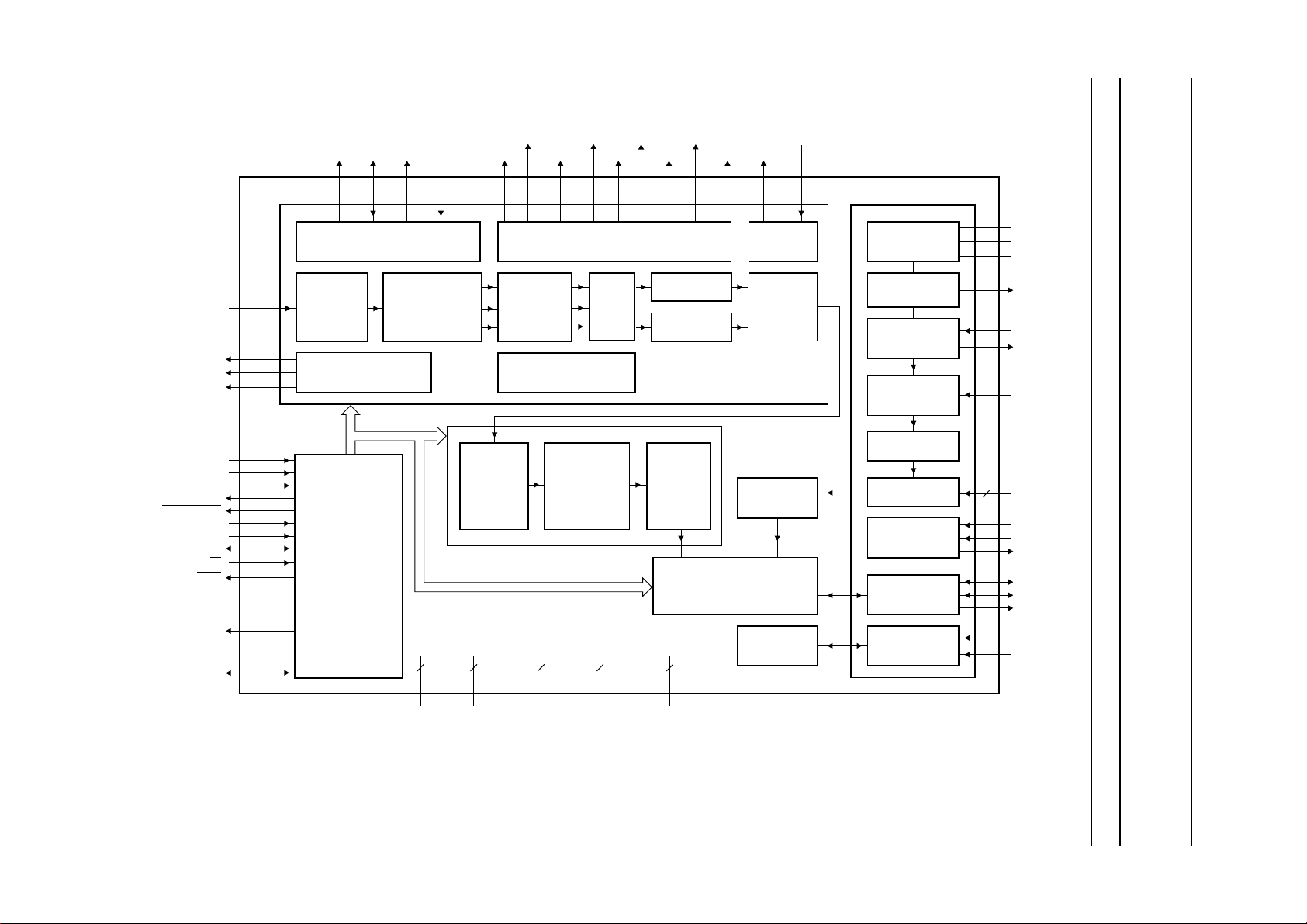
BLOCK DIAGRAM
Digital PC-camera signal processor including
microcontroller and USB interface
Philips Semiconductors Product specification
PXL9 to PXL0
STROBE
SDATA
SCLK
GPI1
GPI2
GPI3
LED
FULLPOWER
SNAPRES
PRIVRES
SDA, SCL
EA
ALE, PSEN
AD14 to AD8
P0.7 to P0.0
11, 12,
13, 14,
15, 16,
17, 18,
19, 20
25
27
26
34
70
71
4
89
28
29
33, 32
54
49, 50
48, 51, 47,
52, 46, 53,
45
39, 38, 40,
37, 41, 35,
42, 36
H
V ASCLK PCLK
VSP
WINDOW TIMING AND
CONTROL REFERENCE TIMING
PRE-
PROCESSING
PRE-PROCESSING
80C51
MICROCONTROLLER
RECONSTRUCTION
INTERFA CE
2
V
DDA1,
V
DDA2
RGB
72, 81
FV1, FV2
VIDEO
FORMA TTER
VFC
3
75, 78, 68
AGND1 to
AGND3
FV3, FV4
RGB
PROCESSING
MEASUREMENT ENGINE
ROG
FH1, FH2
PULSE PATTERN GENERATOR
RGB TO
COMPRESSION
ENGINE
SAA8116
2
V
DDD1,
V
DDD2
56, 21
V
6
DD1
V
DD6
BCP, DCP
CRSTRGFS, FCDS
PROCESSING
YUV
PROCESSING
TRANSFER
BUFFER
8
7, 30, 43,
76, 87, 99
to
8, 31, 44, 77,
88, 100, 55, 22
GND1 to
GND8
SMP RESERVED1
Y
UV
USB
INTERFACE
RESERVED2, RESERVED3
94 64 83, 8423, 245, 692979391, 903, 981, 29109695
MODE
DECODER
4 : 2 : 2
FORMATTER
AUDIO
DECIMATION
POWER
MANAGEMENT
ANALOG MODULES
LDO
SUPPLY
FILTER
MICROPHONE
SUPPLY
AUDIO
LOW NOISE
AMPLIFIER
PROGRAMMABLE
AUDIO GAIN
AMPLIFIER
AUDIO PLL
AUDIO ADC
OSCILLATOR
AND CPLL
ATX
POR
65,
66,
57
58
59
60
61
62
63
67
3
85
74
73
80
79
82
86
69
LDOIN
LDOFIL
LDOOUT
MICSUPPLY
MICIN
LNAOUT
PGAININ
V
ref1,
V
ref2,
V
ref3
XSEL
XIN
XOUT
ATXDP
ATXDN
DELAYATT
PSEL
PORE
FCE673
SAA8116
Fig.1 Block diagram (LQFP100).
This text is here in white to force landscape pages to be rotated correctly when browsing through the pdf in the Acrobat reader.This text is here in
_white to force landscape pages to be rotated correctly when browsing through the pdf in the Acrobat reader.This text is here inThis text is here in
white to force landscape pages to berotated correctly when browsing through the pdf in theAcrobat reader. white to force landscape pages to be...
2001 May 04 5
Digital PC-camera signal processor including
microcontroller and USB interface
Philips Semiconductors Product specification
PXL9 to PXL0
STROBE
SDATA
SCLK
GPI1
GPI2
GPI3
LED
FULLPOWER
SNAPRES
PRIVRES
SDA, SCL
EA
ALE, PSEN
AD14 to AD8
P0.7 to P0.0
F2, F1,
G3, G1,
G2, H3,
H1, H2,
J3, J1
J4
K3
M2
M5
D12
D11
C1
A6
M3
L3
K5, L4
K11
K10, M11
M10, M12,
L10, J9,
K9, L12,
M9
M7, L7, K7,
L6, L8, L5,
M8, K6
H
V ASCLK PCLK
VSP
WINDOW TIMING AND
CONTROL REFERENCE TIMING
PRE-
PROCESSING
PRE-PROCESSING
INTERFA CE
80C51
MICROCONTROLLER
RECONSTRUCTION
2
V
DDA1,
V
DDA2
RGB
C12, B9
E1E3C4A4
FORMA TTER
VFC
3
AGND1 to
AGND3
FV3, FV4
FV1, FV2
VIDEO
FH1, FH2
C2,
D4,
A3
B1
PULSE PATTERN GENERATOR
RGB
PROCESSING
MEASUREMENT ENGINE
SAA8116
2
V
DDD1,
V
DDD2
J11, J2
D9, C10, E11
ROG
CRSTRGFS, FCDS
C6
RGB TO
YUV
COMPRESSION
ENGINE
6
D3, K4, K8,
B11, B7, C3
V
to
DD1
V
DD6
BCP, DCP
D2,
A5B3C5B5,
D1
PROCESSING
PROCESSING
TRANSFER
BUFFER
8
E2, M4, L9, A11,
B6, A2, K12, K1
GND1 to
GND8
SMP RESERVED1
K2,
L1
Y
UV
USB
INTERFACE
RESERVED2, RESERVED3
B4 G10 A8,
FORMATTER
DECIMATION
MANAGEMENT
MODE
DECODER
4 : 2 : 2
AUDIO
POWER
B8
ANALOG MODULES
LDO
SUPPLY
FILTER
MICROPHONE
SUPPLY
AUDIO
LOW NOISE
AMPLIFIER
PROGRAMMABLE
AUDIO GAIN
AMPLIFIER
AUDIO PLL
AUDIO ADC
OSCILLATOR
AND CPLL
ATX
POR
J12
J10
H11
H12
H10
G11
G12
F12,
F11,
E12
C7
B12
C11
A9
A10
C8
A7
D10
3
LDOIN
LDOFIL
LDOOUT
MICSUPPLY
MICIN
LNAOUT
PGAININ
V
ref1,
V
ref2,
V
ref3
XSEL
XIN
XOUT
ATXDP
ATXDN
DELAYATT
PSEL
PORE
MGU263
SAA8116
Fig.2 Block diagram (TFBGA112).

Philips Semiconductors Product specification
Digital PC-camera signal processor including
SAA8116
microcontroller and USB interface
PINNING
SYMBOL PIN
(1)
FV1 1 D4 O vertical CCD transfer pulse output (or general purpose output)
FV2 2 B1 O vertical CCD transfer pulse output (or general purpose output)
FV3 3 C2 O vertical CCD transfer pulse output (or general purpose output)
LED 4 C1 O output to drive LED
FS 5 D2 O data sample-and-hold pulse output to TDA8787A (SHD)
FCDS 6 D1 O preset sample-and-hold pulse output to TDA8787A (SHP)
V
DD1
7 D3 P supply voltage 1 for output buffers
GND1 8 E2 P ground 1 for output buffers
PCLK 9 E1 I pixel input clock
ASCLK 10 E3 O clock 1 (pixelclock) or clock 2(2 × pixel clock) outputfor ADC orCMOS
PXL9 11 F2 I pixel data input; bit9
PXL8 12 F1 I pixel data input; bit8
PXL7 13 G3 I pixel data input; bit 7
PXL6 14 G1 I pixel data input; bit 6
PXL5 15 G2 I pixel data input; bit 5
PXL4 16 H3 I pixel data input; bit 4
PXL3 17 H1 I pixel data input; bit 3
PXL2 18 H2 I pixel data input; bit 2
PXL1 19 J3 I pixel data input; bit 1
PXL0 20 J1 I pixel data input; bit 0
V
DDD2
21 J2 P supply voltage 2 for the digital core
GND8 22 K1 P ground 8 for input buffers and predrivers
BCP 23 K2 O optical black clamp pulse output to TDA8787A
DCP 24 L1 O dummy clamp pulse output to TDA8787A
STROBE 25 J4 O strobe signal output to TDA8787A or general purpose output of the
SCLK 26 M2 O serial clock output to TDA8787A or general purpose output of the
SDATA 27 K3 O serial data output to TDA8787A or general purpose output of the
SNAPRES 28 M3 I snapshot input or remote wake-up trigger input (programmable)
PRIVRES 29 L3 I privacy shutter input or remote wake-up trigger input (programmable)
V
DD2
30 K4 P supply voltage 2 for input buffers and predrivers
GND2 31 M4 P ground 2 for input buffers and predrivers
SCL 32 L4 I/O I
SDA 33 K5 I/O I
GPI1 34 M5 I general purpose input 1 (Port 4; bit 6)
P0.2 35 L5 I/O microcontroller Port 0 bidirectional (data - address); bit 2
P0.0 36 K6 I/O microcontroller Port 0 bidirectional (data - address); bit 0
BALL
(2)
TYPE
(3)
sensor
microcontroller
microcontroller
microcontroller
2
C-bus clock input/output (master/slave)
2
C-bus data input/output (master/slave)
DESCRIPTION
2001 May 04 6

Philips Semiconductors Product specification
Digital PC-camera signal processor including
SAA8116
microcontroller and USB interface
SYMBOL PIN
(1)
P0.4 37 L6 I/O microcontroller Port 0 bidirectional (data - address); bit 4
P0.6 38 L7 I/O microcontroller Port 0 bidirectional (data - address); bit 6
P0.7 39 M7 I/O microcontroller Port 0 bidirectional (data - address); bit 7
P0.5 40 K7 I/O microcontroller Port 0 bidirectional (data - address); bit 5
P0.3 41 L8 I/O microcontroller Port 0 bidirectional (data - address); bit 3
P0.1 42 M8 I/O microcontroller Port 0 bidirectional (data - address); bit 1
V
DD3
43 K8 P supply voltage 3 for output buffers
GND3 44 L9 P ground 3 for output buffers
AD8 45 M9 O microcontroller Port 2 output (address); bit 0
AD10 46 K9 O microcontroller Port 2 output (address); bit 2
AD12 47 L10 O microcontroller Port 2 output (address); bit 4
AD14 48 M10 O microcontroller Port 2 output (address); bit 6
ALE 49 K10 O address latch enable output for external latch
PSEN 50 M11 O program store enable output for external memory (active LOW)
AD13 51 M12 O microcontroller Port 2 output (address); bit 5
AD11 52 J9 O microcontroller Port 2 output (address); bit 3
AD9 53 L12 O microcontroller Port 2 output (address); bit 1
EA 54 K11 I external access select input; internal (HIGH) or external (LOW)
GND7 55 K12 P ground 7 for input buffers and predrivers
V
DDD1
56 J11 P supply voltage 1 for the digital core
LDOIN 57 J12 P analog supply voltage for LDO supply filter
LDOFIL 58 J10 − external capacitor connection (filter of LDO)
LDOOUT 59 H11 − external capacitor connection (internal analog supply voltage for PLL;
MICSUPPLY 60 H12 O microphone supply output
MICIN 61 H10 I microphone input
LNAOUT 62 G11 O low noise amplifier output
PGAININ 63 G12 I programmable gain amplifier input
RESERVED1 64 G10 O test pin 1 (should be floating)
V
ref1
V
ref2
V
ref3
65 F12 I reference voltage 1 (used in the amplifier and the ADC)
66 F11 I reference voltage 2 (used in the ADC)
67 E12 I reference voltage 3 (used in the ADC)
AGND3 68 E11 P analog ground 3 for PLL; amplifier and ADC
PORE 69 D10 I external Power-on reset
GPI2 70 D12 I general purpose input 2 (Port 1; bit 4)
GPI3 71 D11 I general purpose input 3 (Port 3; bit 5)
V
DDA1
72 C12 P analog supply voltage for crystal oscillator (12 MHz, fundamental)
XOUT 73 C11 O oscillator output
XIN 74 B12 I oscillator input
AGND1 75 D9 P analog ground 1 for crystal oscillator
BALL
(2)
TYPE
(3)
program memory
amplifier and ADC)
DESCRIPTION
2001 May 04 7

Philips Semiconductors Product specification
Digital PC-camera signal processor including
SAA8116
microcontroller and USB interface
SYMBOL PIN
V
DD4
(1)
76 B11 P supply voltage 4 for input buffers and predrivers
GND4 77 A11 P ground 4 for input buffers and predrivers
AGND2 78 C10 P analog ground 2 for ATX transceiver
ATXDN 79 A10 I/O negative driver of the differential data pair input/output (ATX)
ATXDP 80 A9 I/O positive driver of the differential data pair input/output (ATX)
V
DDA2
81 B9 P analog supply voltage 2 for ATX transceiver
DELAYATT 82 C8 O delayedattach control output; connected withpull-up resistor onATXDP
RESERVED2 83 A8 I test pin 2 (should be connected to GND)
RESERVED3 84 B8 I test pin 3 (should be connected to GND)
XSEL 85 C7 I crystal selection input
PSEL 86 A7 I POR selection input
V
DD5
87 B7 P supply voltage 5 for output buffers
GND5 88 B6 P ground 5 for output buffers
FULLPOWER 89 A6 O full power signal output (active LOW)
FH2 90 C6 O horizontal CCD transfer pulse output
FH1 91 B5 O horizontal CCD transfer pulse output
RG 92 A5 O reset output for CCD output amplifier gate
ROG 93 C5 O vertical CCD load pulse output
SMP 94 B4 O switch mode pulse output for CCD supply
H 95 A4 O horizontal synchronization pulse output
V 96 C4 I/O vertical synchronization pulse input/output
CRST 97 B3 O CCD charge reset output for shutter control
FV4 98 A3 O vertical CCD transfer pulse output
V
DD6
99 C3 P supply voltage 6 for output buffers
GND6 100 A2 P ground 6 for output buffers
BALL
(2)
TYPE
(3)
DESCRIPTION
(USB)
Notes
1. Pinning related to LQFP100 package.
2. Pinning related to TFBGA112 package.
3. I = input; O = output and P = power supply.
2001 May 04 8

Philips Semiconductors Product specification
Digital PC-camera signal processor including
microcontroller and USB interface
handbook, full pagewidth
FV1
FV2
FV3
LED
FS
FCDS
V
DD1
GND1
PCLK
ASCLK
PXL9
PXL8
PXL7
PXL6
PXL5
PXL4
PXL3
PXL2
PXL1
PXL0
V
DDD2
GND8
BCP
DCP
STROBE
DD6
GND6
V
FV4
CRSTVH
99989796959493929190898887868584838281
100
1
2
3
4
5
6
7
8
9
10
11
12
13
14
15
16
17
18
19
20
21
22
23
24
SMP
ROGRGFH1
FH2
SAA8116
DD5
FULLPOWER
GND5
V
PSEL
XSEL
RESERVED3
DDA2
RESERVED2
DELAYATT
V
ATXDP
ATXDN
AGND2
GND4
V
8079787776
SAA8116
DD4
AGND1
75
74
XIN
73
XOUT
V
72
GPI3
71
70
GPI2
PORE
69
AGND3
68
V
67
V
66
ref2
V
65
ref1
RESERVED1
64
PGAININ
63
62
LNAOUT
MICIN
61
MICSUPPLY
60
LDOOUT
59
58
LDOFIL
LDOIN
57
V
56
DDD1
55
GND7
54
EA
AD9
53
AD11
52
5125
AD13
DDA1
ref3
26272829303132333435363738394041424344454647484950
SCL
SCLK
SDATA
SNAPRES
DD2
V
PRIVRES
GND2
SDA
GPI1
P0.2
P0.0
P0.4
Fig.3 Pin configuration (LQFP100).
2001 May 04 9
P0.6
P0.7
P0.5
P0.3
P0.1
DD3
V
GND3
AD8
AD10
AD12
AD14
ALE
FCE674
PSEN

Philips Semiconductors Product specification
Digital PC-camera signal processor including
microcontroller and USB interface
handbook, halfpage
M
L
K
J
H
G
F
E
D
C
B
A
SAA8116ET
246891011121357
SAA8116
FCE778
Fig.4 Ball configuration; bottom view of ball array (TFBGA112).
2001 May 04 10
Philips Semiconductors Product specification
Digital PC-camera signal processor including
microcontroller and USB interface
Pinning for TFBGA112
BALL SYMBOL
A1 n.c.
A2 GND6
A3 FV4
A4 H
A5 RG
A6
FULLPOWER
A7 PSEL
A8 RESERVED2
A9 ATXDP
A10 ATXDN
A11 GND4
A12 n.c.
B1 FV2
B2 n.c.
B3 CRST
B4 SMP
B5 FH1
B6 GND5
B7 V
DD5
B8 RESERVED3
B9 V
DDA2
B10 n.c.
B11 V
DD4
B12 XIN
C1 LED
C2 FV3
C3 V
DD6
C4 V
C5 ROG
C6 FH2
C7 XSEL
C8 DELAYATT
C9 n.c.
C10 AGND2
C11 XOUT
C12 V
DDA1
D1 FCDS
BALL SYMBOL
D2 FS
D3 V
DD1
D4 FV1
D9 AGND1
D10 PORE
D11 GPI3
D12 GPI2
E1 PCLK
E2 GND1
E3 ASCLK
E10 n.c.
E11 AGND3
E12 V
ref3
F1 PXL8
F2 PXL9
F3 n.c.
F10 n.c.
F11 V
F12 V
ref2
ref1
G1 PXL6
G2 PXL5
G3 PXL7
G10 RESERVED1
G11 LNAOUT
G12 PGAININ
H1 PXL3
H2 PXL2
H3 PXL4
H10 MICIN
H11 LDOOUT
H12 MICSUPPLY
J1 PXL0
J2 V
DDD2
J3 PXL1
J4 STROBE
J9 AD11
J10 LDOFIL
J11 V
DDD1
SAA8116
BALL SYMBOL
J12 LDOIN
K1 GND8
K2 BCP
K3 SDATA
K4 V
K5 SDA
K6 P0.0
K7 P0.5
K8 V
K9 AD10
K10 ALE
K11
K12 GND7
L1 DCP
L2 n.c.
L3 PRIVRES
L4 SCL
L5 P0.2
L6 P0.4
L7 P0.6
L8 P0.3
L9 GND3
L10 AD12
L11 n.c.
L12 AD9
M1 n.c.
M2 SCLK
M3 SNAPRES
M4 GND2
M5 GPI1
M6 n.c.
M7 P0.7
M8 P0.1
M9 AD8
M10 AD14
M11
M12 AD13
DD2
DD3
EA
PSEN
2001 May 04 11

Philips Semiconductors Product specification
Digital PC-camera signal processor including
microcontroller and USB interface
FUNCTIONAL DESCRIPTION
The SAA8116 video processor has a very high level of
programmability:118 (8-bit) registers arededicated forthe
Video Signal Processor (VSP), including Pulse Pattern
Generator (PPG) and Measurement Engine (ME), plus
23 registers for the Video Formatter and
Compressor (VFC). The SAA8116 can accept 8 to 10-bit
digital datafrom variousVGA sensors: CCD(progressive)
or CMOS, with or without colour filters (see Table 1).
Synchronization and video windows
CCD SENSOR PULSE PATTERN GENERATOR
The SAA8116 incorporates aPPG function, which can be
used for VGA CCD sensors, see Table 1.
Depending on the sensor type, an external inverter driver
isrequired toconvert the3.3 V pulsesto avoltage suitable
for the CCD sensor used.
Theactive videosize is640 × 480 forVGA. ThetotalH × V
size is 823 × 486 for VGA.
A total of 19 internal registers make a high level of
flexibility available for the PPG.
FLEXIBLE HV TIMING
The PPG module is not used with CMOS sensors. The
SAA8116 provides some flexibility on the frame size to
increase the range of applicable sensors (see Table 1). It
is possible to program the position, width and polarity of
the H and V signals. The output clock for the CMOS
sensor is selectable between single and double pixel
clock, including a programmable polarity.
The HV timing module can serve both as master orslave.
When servingas aslave, the V pulseonly is needed since
the H pulse is internally derived from V by programming
the number of pixels per line.
VIDEO WINDOWS
Several registers allow the definition of the optical black
window, the active video input window, the active video
output window and the measurement windows.
Table 1 Typical SAA8116 compatible sensors
VGA CCD Sony ICX098AK
VGA CMOS Philips UPA1021
Other sensors all sensors that fulfil the following
SENSOR
TYPE
SAA8116
BRAND PART NUMBER
Panasonic MN37771PT
Sharp LZ24BP
Hyundai HV7131B
Photobit PB-0320
criteria:
• B and W; RGB Bayer colour filter
• 8-bit, 9-bit or 10-bit output
• CMOS or CCD sensors
• progressive
2001 May 04 12
Philips Semiconductors Product specification
Digital PC-camera signal processor including
microcontroller and USB interface
Video signal processor
OPTICAL BLACK PROCESSING
The first processing block of the SAA8116 is a digital
clamp(denoted asPRE-PROCESSINGin Fig.1).Itis used
to align the optical black level to zero or to any arbitrary
value.
The average value of the black is measured in the
programmable optical black window and sent to the
microcontroller for adjustment, if necessary. The value
fixed by the microcontroller is subtracted from the
incoming data stream.
The optical black window has a fixed size of 16 pixels
(horizontally) by 128 (vertically); the position of this
window is fully programmable.
Each of the four colour filter inputs has its own offset and
gain.
DEFECT PIXEL CONCEALMENT
Up to 128 Defect Pixel Coordinates (DPC) can be taken
into account forconcealment. The method is basedeither
on a horizontal linear interpolation, or on a copy of a
neighbouring pixel of the same colour.
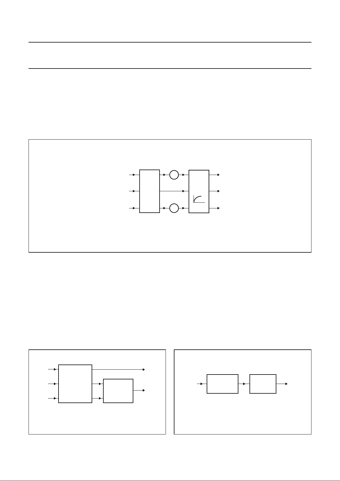
RGB COLOUR RECONSTRUCTOR
In the RGB colour reconstructor (denoted as RGB
RECONSTRUCTION in Fig.1), an RGB triplet is
interpolated for every pixel on a 3 × 3 neighbourhood
matrix.
With B and W sensors, the RGB colour reconstructor can
be disabled, thus maintaining the full sensor resolution.
Vertical contours and video level information (white clip)
are extracted at this stage (see Fig.5).
SAA8116
handbook, full pagewidth
CCD inputs
LINE
MEMORY
RGB
LINE
MEMORY
10
COLOUR
SEPARATION
FCE340
Fig.5 RGB reconstructor diagram.
R
G
B
White clip
Edges
2001 May 04 13
Philips Semiconductors Product specification
Digital PC-camera signal processor including
SAA8116
microcontroller and USB interface
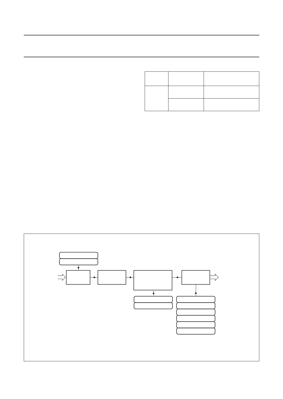
COLOUR MATRIX
A programmable 3 × 3 colour matrix (see Fig.6) is usedto convert the extractedcolour information, R, G and B fromthe
sensor colour space to a standard RGB colour space.
With B and W sensors, a unity matrix is used.
To control the white balance, the gain of the red and blue stream can be changed.
Gamma and knee are combined in one function with adjustable gain.
handbook, full pagewidth
R or (2R-G)
G or Y G
B or (2B-G)
COLOUR
MATRIX
R
B
gain
×
gain
×
R
GAMMA/
KNEE
B
FCE742
Fig.6 RGB processing diagram.
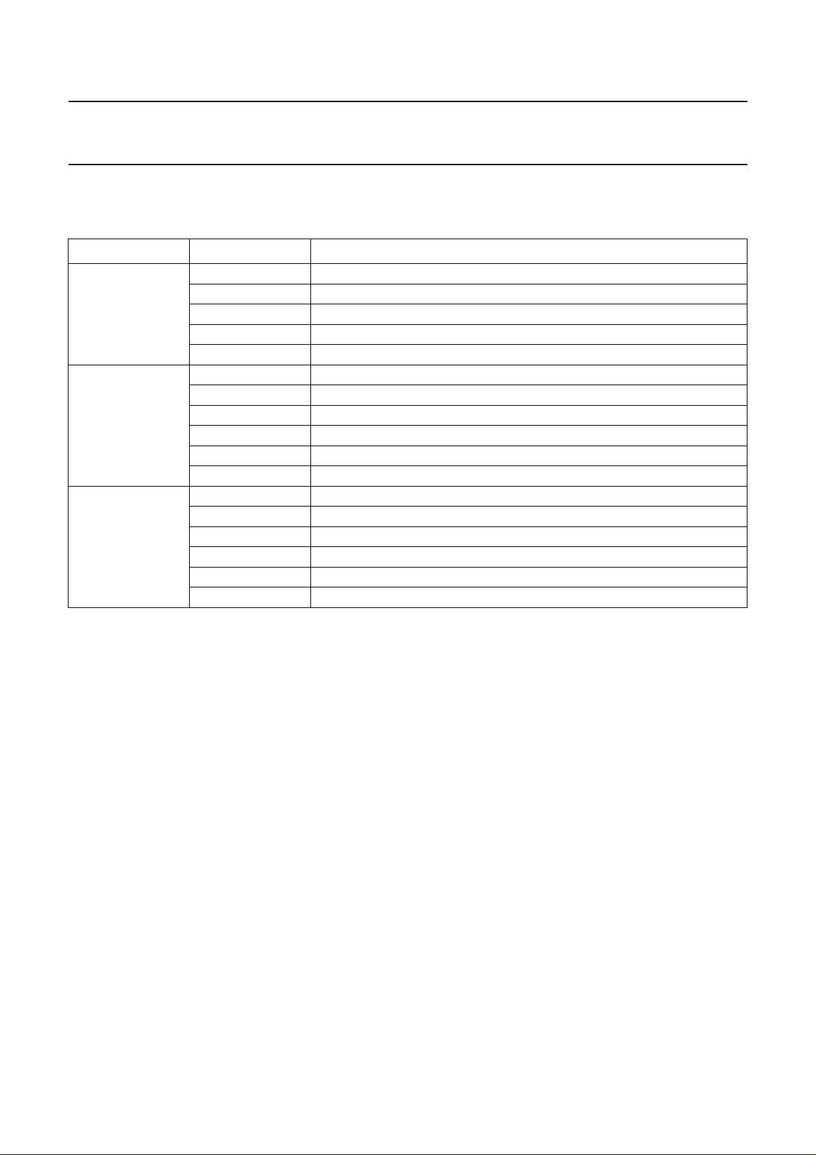
YUV PROCESSING
Following the RGB processing,the R, G and Bsignals are
converted to YUV 4 :2:2 by a fixed matrix (see Fig.7).
Then, the luminance and chrominance signals are
processed separately.
Theluminance processingconsists of edgeenhancement.
Thisfeature isvery flexible.First, itis possibleto adjustthe
bandwidth and the level of the edge detection. Secondly,
the amount of edge enhancement can be independently
adjusted for the horizontal or vertical edge or for the high
or low frequency edge.
R
G
B
CONVERSION
MATRIX
DOWN-
SAMPLING
AND MUX
FCE342
Y
UV
The chrominance processing consists of a colour killer
(white clip) and a UV gain control (see Fig.8). Processing
is done on the multiplexed two-times-downsampled
UV chrominance signals. The sensor input is used to kill
the colour of over-exposed pixels. It is possible to adjust
the number of pixels on which the correction is applied.
The YUV processing block concludes with separate gain
controls on the Y, U and V signals. These gains can be
used to fine tune the Y, U and V colour balance and also
to adjust the luminance and saturation without disturbing
the AE and AWB control loops.
handbook, halfpage
UV
WHITE CLIP
UV GAIN
CONTROL
FCE743
UV
Fig.7 RGB to YUV conversion.
2001 May 04 14
Fig.8 UV processing.
Philips Semiconductors Product specification
Digital PC-camera signal processor including
microcontroller and USB interface
MEASUREMENT ENGINE
The ME extracts statistical information from the video
stream. These measurements are used for the
auto-control loops in the microcontroller (AWB, AE
and AGC).They canalso beusedfor otherpurposes,such
as colourdetection. The measurements areperformed on
pre-formatted Y, U and V streams. It is possible to
measure the accumulated value of the Y, U or V samples
either in the full active video window or in a simple
programmable window.
Five parallelmeasurements ofthe luminance canbe done
for the auto exposure, each based on a proper window.
Y, U and V can be measured independently for the auto
white balance, all based on the same window.
During each frame, the microcontroller has access to the
measured values of the previous frame.
Video formatter
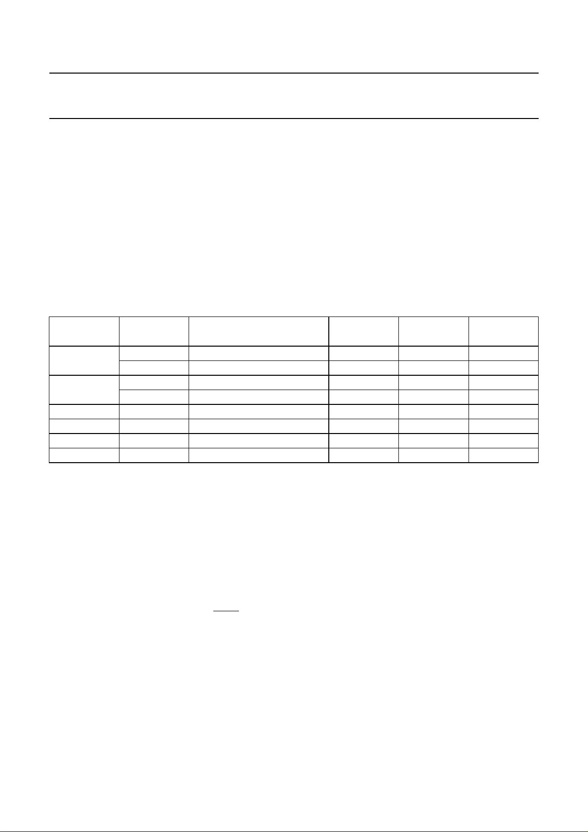
This block is used to convert the YUV 4 : 2 : 2 format to
4:2:0 required by the compression engine. The
incoming 4:2:2 data is vertically filtered. In raw mode,
this block is bypassed to create a full resolution snapshot.
The formatter can also perform downscaling to SIF and
QSIF (see Table 2).
Table 2 Scaler modes
SENSOR
VGA SIF 320 × 240 scaled half horizontally
Compression engine
The compression engine module (see Fig.9) can process
VGA, SIF and QSIF, based on a Philips proprietary
algorithm. The compression ratio is continuously
programmable by setting a maximum bit cost limit. Input
data can also be a raw RGB sensor data to perform
optimum snapshot processing in the host software.
The compression engine uses several strategies and
Q-tables for optimum performance at a wide range of
compression ratios (upto 8×). The required table must be
selected via software. One table is optimized for
compressing the raw VGA data.
Real time decoding can be done in software on any
Pentium or AMD-K6 platform.
TYPE
SAA8116
OUTPUT
FORMAT
QSIF 160 × 120 scaled quarter
SCALER MODES
and vertically
horizontally and vertically
To avoid aliasing, this formatter also contains horizontal
and vertical low pass pre-filters before downscaling.
handbook, full pagewidth
YUV7 to
YUV0
PREFILTER_SEL_UV
PREFILTER_SEL_Y
PREFILTER
HORIZONTAL
DOWNSCALING
Fig.9 The video formatter and compression engine.
DATA FORMATTER
+
VERTICAL
DOWN SAMPLING
VF_LIMITER
SCALE_DATA
COMPRESSION
ENGINE
TABLE_SELECT
LDC
C_BITCOST_MSB
C_BITCOST_LSB
C_THRESHOLD_MSB
C_THRESHOLD_LSB
FCE744
to
transfer
buffer
2001 May 04 15
Philips Semiconductors Product specification
Digital PC-camera signal processor including
microcontroller and USB interface
Table 3 gives the available output formats and frame rates.
Table 3 Video formats
FORMAT FRAME RATE COMPRESSION MODE
VGA 5 raw; compressed
5 compressed
10 compressed
15 compressed
30 compressed
SIF 5 compressed and uncompressed
10 compressed
15 compressed
20 compressed
24 compressed
30 compressed
QSIF 5 compressed and uncompressed
10 compressed and uncompressed
15 compressed and uncompressed
20 compressed and uncompressed
24 compressed and uncompressed
30 compressed and uncompressed
SAA8116
The compressed data is streamed into a video FIFO, ready to be packed into USB formatted data blocks.
2001 May 04 16
Philips Semiconductors Product specification
Digital PC-camera signal processor including
microcontroller and USB interface
Universal serial bus 1.1 core
The USB core combines all functionalities for a USB 1.1
compliant full speed device. It formats the actual packets
(video and audio) that are transferred to the USB and
passes the incoming packetsto the right end-point buffer.
The end-point setup is composed of control, generic and
isochronous types (see Table 4). All end-points can be
enabled or disabled, except control end-points.
All enabled end-points generate interrupts to the
embedded microcontrollerwhen theyneed tobe serviced.
The microcontroller can then use a set of commands via
the internal parallel interface.
Table 4 Mapping of logical to physical end-point numbers for the end-points
LOGICAL
END-POINT
0 0 control out 16 no
1 2 generic out 8 no
2 4 generic in 8 no
3 5 generic in 8 no
4 6 isochronous in 92 yes
5 7 isochronous in programmable multi-buffered
PHYSICAL
END-POINT
1 control in 16 no
3 generic in 8 no
END-POINT TYPE DIRECTION BUFFER SIZE
The video FIFO size allows demarcation of the video
frames using one or more 0-length packets.
The core also includes VID class support for the video
end-point: headersand trailersenable data tobe attached
to the video frames that are passed over the USB. Eight
1-byte registers are dedicated for the headers, while four
registerscomprise thetrailers. Eachofthe registerscanbe
programmed by the microcontroller. An extra register,
TR_HT_CONTROL, specifies how many bytes are
inserted before or after the video data.
SAA8116
DOUBLE
BUFFERED
ATX interface
The SAA8116 contains an analog bus driver, called
the ATX. This driver incorporates a differential amplifier
and twosingle-ended buffers for thereceiver part and two
single-ended buffers for the transmitter part.
The interface to the bus consists of a differential data pair
(ATXDN and ATXDP).
Microcontroller
The embeddedmicrocontroller is an 80C654core (80C51
family). Ports P0 and P2 (plus ALE and PSEN) are
available for connection to an emulator or to an external
program EPROM (32 kbytes max.).
The microcontroller can control the AOB, AE and AWB
loops, and can download the settings for the internal
registers from an optional EEPROM at power-up or reset.
Aparallel interfaceis usedto communicatewith allinternal
modules, based on the MOVX@DPTR instruction.
The microcontroller includes the following features:
• 32 kbytes internal ROM
• 512 bytes RAM
• Hardware multi-master I2C-bus interface (the
microcontroller can be used either as slave or master):
P1.7 and P1.6
• Power-down mode
• Two timers
• P0 and P2 are pull-up ports
• Three pins are available as general purpose inputs:
GPI1 (P4.6), GPI2 (P1.4) and GPI3 (P3.5).
2001 May 04 17
Philips Semiconductors Product specification
Digital PC-camera signal processor including
SAA8116
microcontroller and USB interface
Table 5 80C51 Special Function Registers (SFR)
SFR
NAME
B B register F0H B7 B6 B5 B4 B3 B2 B1 B0
ACC accumulator E0H ACC7 ACC6 ACC5 ACC4 ACC3 ACC2 ACC1 ACC0
SIADR serial interface address DBH SA6 SA5 SA4 SA3 SA2 SA1 SA0 GC
SIDAT serial interface data DAH SD7 SD6 SD5 SD4 SD3 SD2 SD1 SD0
SISTA serial interface status D9H ST7 ST6 ST5 ST4 ST3 0 0 0
SICON serial interface control D8H CR2 ENS1 STA STO SI AA CR1 CR0
PSW program status word D0H CY AC F0 RS1 RS0 OV − P
P4 Port 4 C0H P4.7 P4.6 P4.5 P4.4 P4.3 P4.2 P4.1 P4.0
IP interrupt priority B8H − IP6 IP5 IP4 PT1 PX1 PT0 PX0
P3 Port 3 B0H
IE interrupt enable A8H
P2 Port 2 A0H (AD15) AD14 AD13 AD12 AD11 AD10 AD9 AD8
SBUF serial data buffer 99H −−−−−−−−
SCON serial controller 98H SM0 SM1 SM2 REN TB8 RB8 T1 R1
P1 Port 1 90H SDA SCL P1.5 P1.4 P1.3 P1.2 P1.1 P1.0
TH1 timer high 1 8DH −−−−−−−−
TH0 timer high 0 8CH −−−−−−−−
TL1 timer low 1 8BH −−−−−−−−
TL0 timer low 0 8AH −−−−−−−−
TMOD timer mode 89H GATE C/T M1 M0 GATE C/T M1 M0
TCON timer control 88H TF1 TR1 TF0 TR0 IE1 IT1 IE0 IT0
PCON power control 87H −−−−−−PD IDL
DPH data pointer high 83H −−−−−−−−
DPLl data pointer low 82H −−−−−−−−
SP stack pointer 81H SP7 SP6 SP5 SP4 SP3 SP2 SP1 SP0
P0 Port 0 80H P0.7 P0.6 P0.5 P0.4 P0.3 P0.2 P0.1 P0.0
DESCRIPTION
SFR
ADDRESS
76543210
RD WR T1 T0 INT1 INT0 TXD RXD
EA IE6 IE5 IE4 ET1 EX1 ET0 EX0
DATA BIT
Audio
The SAA8116 contains a microphone supply, including a
low-drop electronic supply filter, and an amplifier circuit
composedof twostages: aLow NoiseAmplifier (LNA) and
a variable gain amplifier (VGA).The LNA has a fixed gain
of 30 dB while the VGA can be programmed between
0 and 30 dB in steps of 2 dB. The frequency transfer
characteristic of the audio path must be controlled via
external high-pass or low-pass filters.
2001 May 04 18
The PLL converts the 48 MHz to 256fs(fs= audio sample
frequency). There arethree modes for the PLL toachieve
the sample frequencies of 48, 44.1 and 32 kHz or their
derivatives (see Table 6).
Thebitstream ADCsamples themono audiosignal. Itruns
at an oversample rate of 256 times the base sample rate.
A decimator filtertransforms the bitstream outputto 16-bit
samples.
A digital mute option is available.
 Loading...