

Philips saa8115hl DATASHEETS

SAA8115HL
Digital camera USB interface
Rev. 04 — 10 August 2000 Product specification
1. General description
The SAA8115HL is the second generation of integrated circuit applicableinPC video
cameras to convert D1 video signals and analog audio signals to properly formatted
USB packets.
This powerful successor of the SAA8117HL can handle up to 15 fps in VGAformat or
30 fps in CIF format. High snapshot quality is achievable using the SDRAM interface
to an external memory.
It is designed as a back-end of the SAA8112HL (general camera digital
processing IC) and is optimized for use with the TDA8784 to TDA8787 (camera
pre-processing ICs).
2. Features
■ VGA (progressive mode), CIF and medium resolution (PAL non-interlaced mode)
CCD sensors compliant
■ D1 digital video input (8 bits YUV4:2:2time multiplexed)
c
c
■ Internal Pulse Pattern Generator (PPG) dedicated for VGA Panasonic, CIF and
medium resolution Sharp sensors or compatibles, and frame rate selection
■ Frame rate converter
■ SDRAM interface for high quality VGA snapshot (uncompressed 4 :2:2 or
4:2:0)
■ Downsampler and scaler (programmable formatter for CIF, QCIF, sub-QCIF, SIF
and QSIF) controlled via SNERT (UART) interface
■ Flexible compression engine controlled via SNERT (UART) interface
■ Selectable output frame rate (up to 15 fps in VGA, up to 30 fps in CIF and QCIF)
■ Video packetizer FIFO
■ I2C-bus interface for communication between the USB protocol hardware and the
external microcontroller
■ Microphone/audio input to USB (microphone supply, controllable gain and ADC)
■ Integrated analog bus driver (ATX)
■ Integrated main oscillator
■ Integrated 5 V power supply and reset circuit including functionalities for
bus-powered USB device
■ Programmable (frequency and duty cycle) switch mode power signal for CCD
supply

Philips Semiconductors
SAA8115HL
Digital camera USB interface
■ Miscellaneous functions (e.g. power management, PLL for audio frequencies).
3. Applications
■ Low-cost desktop video applications with USB interface.
4. Quick reference data
Table 1: Quick reference data
Measured over full voltage and temperature range
Symbol Parameter Conditions Min Typ Max Unit
V
DDD
V
DDA
V
DDA(USB)
I
DD
I
DD(DC-DC)
V
I
V
O
f
clk
T
stg
T
amb
T
j
digital supply voltage 3.0 3.3 3.6 V
analog supply voltage 3.0 3.3 3.6 V
analog supply voltage from USB
supply current
DC-DC supply current
input signal levels 3.0 V < V
output signal levels 3.0 V < V
< 3.6 V low voltage TTL compatible V
DDD
< 3.6 V low voltage TTL compatible V
DDD
[1]
4.3 5.0 5.5 V
[2]
− 100 125 mA
[3]
− 240 320 mA
clock frequency − 48 − MHz
storage temperature −55 −−°C
ambient temperature 0 25 70 °C
junction temperature T
=70°C −40 − +125 °C
amb
[1] This concerns pins VBUS1 and VBUS2.
[2] Conditions:
a) typical: VGA at 15 fps; V
b) maximum: VGA at 30 fps; V
[3] Conditions (I
a) typical: V
b) maximum: V
= 125 mA):
OUT
DD(USB)
DD(USB)
= 5.0 V; T
= 4.3 V; T
DDD=VDDA
DDD=VDDA
amb
=25°C
=70°C.
amb
= 3.3 V; T
= 3.6 V; T
amb
=25°C
=70°C.
amb
5. Ordering information
Table 2: Ordering information
Type number Package
Name Description Version
SAA8115HL LQFP144 plastic low profile quad flat package; 144 leads; body 20 × 20 × 1.4 mm SOT486-1
9397 750 07395
Product specification Rev. 04 — 10 August 2000 2 of 51
© Philips Electronics N.V. 2000. All rights reserved.

9397 750 07395
Product specification Rev. 04 — 10 August 2000 3 of 51
6. Block diagram
Philips Semiconductors
DDD3
to V
AD10
to AD0
DQ15
to DQ0
YUV7
to YUV0
LLC
HREF
SNDA
SNCL
SNRES
48, 47, 45, 44,
42, 39, 38, 40,
41, 43, 46
77, 76, 75, 74, 67, 65,
62, 60, 61, 63, 64, 66,
70, 71, 72, 73
28, 27, 26, 25
22, 21, 20, 19
30
31
32
VS
34
35
36
DDD1
V
24,
53,
102
CASB
RASB52SDCLK
WEB57CLKEN55CSB
56
58
SDRAM
INTERFACE
FRAME RATE
CONVERTER
SNERT
INTERFACE
DQM
51
59
FORMATTER
VIDEO
hhhhhhhhhhhhhhhhhhhhhhhhhhhhhhhhhhhhhhhhhhhhhhhhhhhhhhhhhhhhhhhhhhhhhhhhhhhhhhhhhhhhhhhhh
hhhhhhhhhhhhhhhhhhhhhhhhhhhhhhhhhhhhhhhhhhhhhhhhhhhhhhhhhhhhhhhhhhhhhhhhhhhhhhhhhhhhhhhhh
hhhhhhhhhhhhhhhhhhhhhhhhhhhhhhhhhhhhhhhhhhhhhhhhhhhhhhhhhhhhhhhhhhhhhhhhhhhhhhhhhhhhhhhhh
139, 140,
hhhhhhhhhhhhhhhhhhhhhhhhhhhhhhhhhhhhhhhhh
143, 144
© Philips Electronics N.V. 2000. All rights reserved.
A1 to A4
PULSE PATTERN GENERATOR
137, 138,
136, 135
B1 to B4
3, 2,
1, 4
C1 to C4
(PPG)
5RG8
SHUTTER
10FS9
FCDS
12
DCP
13
BCP
DD6
to V
DD1
V
7, 16,
37, 50,
69, 141
DDA6
to V
DDA1
V
82, 84,
85, 122,
124, 125
COMPRESSION
ENGINE
17
11HD15VD14
CLK1
CLK2
M3 to M0
RESET
DGND1 to DGND4
115, 116,
33
23, 29,
54, 101
117, 118
TRANSFER
BUFFER
SAA8115HL
DC-TO-DC CONVERTER
94
92
91
90
87
3V3
VBUS1
VBUS2
LXUP
LXDOWN
AGND1 to AGND6
79, 88,
93, 119,
123, 134
114
113
95
OFF
POR
SWITCHED5V
GND1 to GND7
6, 18,
49, 68,
78, 98,
142
USB
VIDEO
FIFO
MAIN
OSCILLATOR
121
120
XIN
RESERVED1 to
RESERVED6
REF1 to REF3
83, 86,
126,
89, 96,
127,
97, 129
128
USB
RAM
SPACE
AUDIO
MICROPHONE
SUPPLY
XOUT
PLL
133
MICSUPPLY
SUSPEND
GENPOR
100 109
103
POWER MANAGEMENT
PSIE MMU
AUDIO
ADC
AUDIO
VARIABLE
GAIN
AMPLIFIER
AUDIO
LOW NOISE
AMPLIFIER
132
MICIN
CLOCKON
TRC
112
SNAPSHOT
SUSPREADYNOT
110
111
ATX
2
C-BUS
I
INTERFACE
SMP
108
99
104
105
80
81
106
107
130
131
FCE349
UCINT
UCPOR
UCCLK
ATXDP
ATXDM
SCL
SDA
VGAIN
LNAOUT
Digital camera USB interface
SAA8115HL
Fig 1. Block diagram.
Philips Semiconductors
7. Pinning information
7.1 Pinning
SAA8115HL
Digital camera USB interface
SHUTTER
GND1
V
DD1
RG
FCDS
CLK1
DCP
BCP
VD
HD
V
DD2
CLK2
GND2
YUV0
YUV1
YUV2
YUV3
DGND1
V
DDD1
YUV4
YUV5
YUV6
YUV7
DGND2
LLC
HREF
RESET
SNDA
SNCL
SNRES
DD6
A4A3GND7
V
A2A1B2B1B3B4AGND6
144
143
142
141
140
139
138
137
1
C3
2
C2
3
C1
C4
4
5
6
7
8
FS
9
10
11
12
13
14
15
16
17
18
19
20
21
22
23
24
25
26
27
28
29
30
31
32
VS
33
34
35
36
3738394041424344454647484950515253545556575859606162636465666768697071
AD4
AD5
AD3
AD2
AD6
AD1
V
DD3
AD7
136
AD8
135
AD0
MICSUPPLY
134
133
AD9
AD10
MICIN
132
GND3
LNAOUT
VGAIN
131
130
DD4
CSB
V
RESERVED6
129
SAA8115HL
RASB
REF3
128
DDD2
V
REF2
REF1
127
126
CLKEN
DGND3
DDA6VDDA5
V
125
124
WEB
CASB
DDA4
AGND5
V
123
122
DQM
SDCLK
XOUT
121
DQ8
XIN
120
DQ7
AGND4M0M1M2M3
119
118
117
116
DQ9
DQ6
DQ5
DQ10
115
DQ4
OFF
114
DQ11
POR
113
GND4
TRC
SUSPREADYNOT
SNAPSHOT
112
111
110
DD5
DQ3
DQ2
V
CLOCKON
109
108
107
106
105
104
103
102
101
100
99
98
97
96
95
94
93
92
91
90
89
88
87
86
85
84
83
82
81
80
79
78
77
76
75
74
73
72
DQ1
SMP
SDA
SCL
UCCLK
UCPOR
GENPOR
V
DDD3
DGND4
SUSPEND
UCINT
GND6
RESERVED5
RESERVED4
SWITCHED5V
LXUP
AGND3
LXDOWN
VBUS2
VBUS1
RESERVED3
AGND2
3V3
RESERVED2
V
DDA3
V
DDA2
RESERVED1
V
DDA1
ATXDM
ATXDP
AGND1
GND5
DQ15
DQ14
DQ13
DQ12
DQ0
FCE350
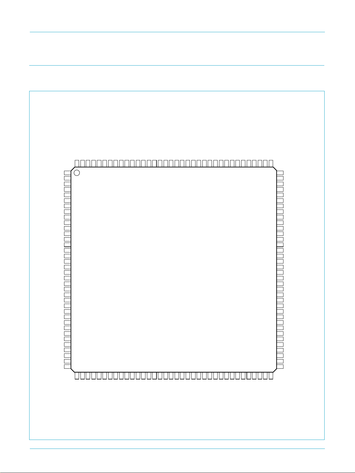
Fig 2. Pin configuration.
9397 750 07395
Product specification Rev. 04 — 10 August 2000 4 of 51
© Philips Electronics N.V. 2000. All rights reserved.

Philips Semiconductors
7.2 Pin description
Table 3: Pin description
Symbol Pin Type
C3 1 O horizontal CCD transfer pulse output
C2 2 O horizontal CCD transfer pulse output (FH1)
C1 3 O horizontal CCD transfer pulse output (FH2)
C4 4 O horizontal CCD transfer pulse output
SHUTTER 5 O shutter control output for CCD charge reset
GND1 6 P ground 1 for output buffers
V
DD1
RG 8 O reset output for CCD output amplifier gate
FS 9 O data sample-and-hold pulse output to TDA8784/87 (SHD)
FCDS 10 O preset sample-and-hold pulse output to TDA8784/87
CLK1 11 O pixel clock to TDA8784/87 and SAA8112HL
DCP 12 O dummy clamp pulse output to TDA8784/87
BCP 13 O optical black clamp pulse output to TDA8784/87
VD 14 O vertical definition pulse to SAA8112HL
HD 15 O horizontal definition pulse to SAA8112HL
V
DD2
CLK2 17 O double pixel clock to SAA8112HL
GND2 18 P ground 2 for output buffers
YUV0 19 I multiplexed YUV bit0
YUV1 20 I multiplexed YUV bit1
YUV2 21 I multiplexed YUV bit2
YUV3 22 I multiplexed YUV bit3
DGND1 23 P digital ground 1 for input buffers, predrivers and for the
V
DDD1
YUV4 25 I multiplexed YUV bit4
YUV5 26 I multiplexed YUV bit5
YUV6 27 I multiplexed YUV bit6
YUV7 28 I multiplexed YUV bit7
DGND2 29 P digital ground 2 for input buffers, predrivers and for the
LLC 30 I line-locked clock input (delayed CLK2) for YUV-port from
HREF 31 I horizontal reference input for YUV-port from SAA8112HL
VS 32 I vertical synchronization input for YUV-port from
RESET 33 I Power-on reset input (for video processing and PPG)
SNDA 34 I/O data input/output for SNERT-interface (communication
SAA8115HL
Digital camera USB interface
[1]
Description
7 P supply voltage 1 for output buffers
(SHP)
16 P supply voltage 2 for output buffers
digital core
24 P digital supply voltage 1 for input buffers, predrivers and
one part of the digital core
digital core
SAA8112HL
SAA8112HL
between SAA8115HL and SAA8112HL)
9397 750 07395
Product specification Rev. 04 — 10 August 2000 5 of 51
© Philips Electronics N.V. 2000. All rights reserved.

Philips Semiconductors
SAA8115HL
Digital camera USB interface
Table 3: Pin description
Symbol Pin Type
…continued
[1]
Description
SNCL 35 I clock input for SNERT-interface (communication between
SAA8115HL and SAA8112HL)
SNRES 36 I reset input for SNERT-interface (communication between
SAA8115HL and SAA8112HL)
V
DD3
37 P supply voltage 3 for output buffers
AD4 38 O SDRAM output address bit 4
AD5 39 O SDRAM output address bit 5
AD3 40 O SDRAM output address bit 3
AD2 41 O SDRAM output address bit 2
AD6 42 O SDRAM output address bit 6
AD1 43 O SDRAM output address bit 1
AD7 44 O SDRAM output address bit 7
AD8 45 O SDRAM output address bit 8
AD0 46 O SDRAM output address bit 0
AD9 47 O SDRAM output address bit 9
AD10 48 O SDRAM output address bit 10
GND3 49 P ground 3 for output buffers
V
DD4
50 P supply voltage 4 for output buffers
CSB 51 O SDRAM chip select output
RASB 52 O SDRAM row address strobe output
V
DDD2
53 P digital supply voltage 2 for the switchable digital core
DGND3 54 P digital ground 3 for input buffers, predrivers and for the
digital core
CLKEN 55 O SDRAM clock enable output
CASB 56 O SDRAM column address strobe output
WEB 57 O SDRAM write enable output
SDCLK 58 O SDRAM clock output
DQM 59 I/O SDRAM data mask enable
DQ8 60 I/O SDRAM data I/O bit 8
DQ7 61 I/O SDRAM data I/O bit 7
DQ9 62 I/O SDRAM data I/O bit 9
DQ6 63 I/O SDRAM data I/O bit 6
DQ5 64 I/O SDRAM data I/O bit 5
DQ10 65 I/O SDRAM data I/O bit 10
DQ4 66 I/O SDRAM data I/O bit 4
DQ11 67 I/O SDRAM data I/O bit 11
GND4 68 P ground 4 for output buffers
V
DD5
69 P supply voltage 5 for output buffers
DQ3 70 I/O SDRAM data I/O bit 3
DQ2 71 I/O SDRAM data I/O bit 2
DQ1 72 I/O SDRAM data I/O bit 1
9397 750 07395
Product specification Rev. 04 — 10 August 2000 6 of 51
© Philips Electronics N.V. 2000. All rights reserved.

Philips Semiconductors
SAA8115HL
Digital camera USB interface
Table 3: Pin description
Symbol Pin Type
…continued
[1]
Description
DQ0 73 I/O SDRAM data I/O bit 0
DQ12 74 I/O SDRAM data I/O bit 12
DQ13 75 I/O SDRAM data I/O bit 13
DQ14 76 I/O SDRAM data I/O bit 14
DQ15 77 I/O SDRAM data I/O bit 15
GND5 78 P ground 5 for output buffers
AGND1 79 P analog ground 1 for ATX (transceiver)
ATXDP 80 I/O positive driver of the differential data pair input/output
(ATX)
ATXDM 81 I/O negative driver of the differential data pair input/output
(ATX)
V
DDA1
82 P analog supply voltage 1 for ATX
RESERVED1 83 − test pin 1 (should not be used)
V
V
DDA2
DDA3
84 P analog supply voltage 2 for bandgap (reference)
85 P analog supply voltage 3 for bandgap, comparator and ring
oscillator
RESERVED2 86 − test pin 2 (should not be used)
3V3 87 I 3V3 detector input signal
AGND2 88 P analog ground 2 for N-switch
RESERVED3 89 − test pin 3 (should not be used)
VBUS1 90 I supply voltage input 1 from the USB
VBUS2 91 I supply voltage input 2 from the USB
LXDOWN 92 O LX coil node output (5 V downconverter)
AGND3 93 P analog ground 3 for N-switch
LXUP 94 I LX coil node input (5 V upconverter)
SWITCHED5V 95 O 5 V switched power supply
RESERVED4 96 − test pin 4 (should not be used)
RESERVED5 97 − test pin 5 (should not be used)
GND6 98 P ground 6 for output buffers
UCINT 99 O interrupt output from USB to microcontroller
SUSPEND 100 O control output from USB protocol hardware to
microcontroller
DGND4 101 P digital ground 4 for input buffers, predrivers and for the
digital core
V
DDD3
102 P digital supply voltage 3 for input buffers, predrivers and
one part of the digital core
GENPOR 103 I Power-on reset input (for USB protocol hardware)
UCPOR 104 O control output from USB protocol hardware to
microcontroller
UCCLK 105 O clock output from USB protocol hardware to
microcontroller
2
SCL 106 I slave I
SDA 107 I/O slave I
C-bus clock input
2
C-bus data input/output
9397 750 07395
Product specification Rev. 04 — 10 August 2000 7 of 51
© Philips Electronics N.V. 2000. All rights reserved.

Philips Semiconductors
SAA8115HL
Digital camera USB interface
Table 3: Pin description
Symbol Pin Type
…continued
[1]
Description
SMP 108 O switch mode power pulse output for CCD supplies
CLOCKON 109 O control output for main oscillator switched on
SNAPSHOT 110 I input for remote wake-up (snapshot)
SUSPREADYNOT 111 I input from microcontroller for SUSPEND mode
TRC 112 I threshold control input for enabling clock
POR 113 O 3.3 V supply domain ready indicator output
OFF 114 I disable 5 V switchable supply domain input
M3 115 I test mode control input signal bit 3
M2 116 I test mode control input signal bit 2
M1 117 I test mode control input signal bit 1
M0 118 I test mode control input signal bit 0
AGND4 119 P analog ground 4 for crystal oscillator (48 MHz,
3rd overtone)
XIN 120 I oscillator input
XOUT 121 O oscillator output
V
DDA4
122 P analog supply voltage 4 for crystal oscillator (48 MHz,
3rd overtone)
AGND5 123 P analog ground 5 for PLL
V
V
DDA5
DDA6
124 P analog supply voltage 5 for PLL
125 P analog supply voltage 6 for amplifier and ADC
REF1 126 I reference voltage 1 (used in the ADC)
REF2 127 I reference voltage 2 (used in the ADC)
REF3 128 I reference voltage 3 (used in the amplifier and the ADC)
RESERVED6 129 O test pin 6 (should not be used)
VGAIN 130 I variable gain amplifier input
LNAOUT 131 O low noise amplifier output
MICIN 132 I microphone input
MICSUPPLY 133 O microphone supply output
AGND6 134 P analog ground 6 for amplifier and ADC
B4 135 O vertical CCD load pulse output (VH1X)
B3 136 O vertical CCD load pulse output (VH3X)
B1 137 O vertical CCD load pulse output
B2 138 O vertical CCD load pulse output
A1 139 O vertical CCD transfer pulse output (V1X)
A2 140 O vertical CCD transfer pulse output (V2X)
V
DD6
141 P supply voltage 6 for output buffers
GND7 142 P ground 7 for output buffers
A3 143 O vertical CCD transfer pulse output (V3X)
A4 144 O vertical CCD transfer pulse output (V4X)
[1] I = input, O = output and P = power supply.
9397 750 07395
Product specification Rev. 04 — 10 August 2000 8 of 51
© Philips Electronics N.V. 2000. All rights reserved.

Philips Semiconductors
8. Functional description
8.1 Video synchronization
The video synchronization module is capable of locking to the video signal
implementing a horizontal gate signal HREF (HREF = HIGH when data is valid)and a
VS signal indicating the start of a new video frame.
8.2 Frame rate converter and SDRAM interface
An optional SDRAM (external) can be accessed using the SDRAM interface which is
integrated in the SAA8115HL. Pinning and functionality is based on the NEC
µPD4516161 (16 Mbits) and the NEC µPD4564163 (64 Mbits).
When used, the memory is placed at the video input of the SAA8115HL before
prefilter, scaler and compression engine. At this point only YUV 4 :2:2 formatted
data is available.
The use of the SDRAM is twofold:
SAA8115HL
Digital camera USB interface
Lowering the frame rate. The memory enables to store one frame of video
•
accumulated at a specific rate and to read it out at a lower frame rate. For interline
VGA sensors, the input frame rate is either 30 fps or 15 fps. It can be lowered with
a factor of 2, 3, 6, 16 or 32. For CIF or medium resolution PAL, the input frame rate
is only 30 fps
Enhanced snapshot mode. Storage of full size VGA pictures in 4:2:2 format
•
which can be retrieved upon dedicated software command.
8.3 Video formatter: downsampler and cutter
This block is used to achieve the required output format from the specified sensor
formats (see Figure 3). It works for YUV 4:2:2 only. In RAW mode this block is
by-passed to create a full resolution snapshot.
Horizontally a downsampling from 512 or 640 to either 384, 320, 192 or 160 or from
352 to 176 is necessary. The horizontal downsampling is performed with the use of a
Variable Phase Delay filter (VPD-4). This filter can realize the needed downsample
factors. To avoid aliasing, this module also contains a prefilter which has four modes:
No filter for medium resolution PAL (512 × 288) to CIF (352 × 288) or SIF
•
(320 × 240)
Prefilter A (3 taps) for VGA (640 × 480) to CIF or SIF, CIF to QCIF (176 × 144) or
•
QSIF (160 × 120)
Prefilter B (7 taps) for medium resolution PAL to QCIF or QSIF
•
Prefilter A combined with prefilter B-comb (13 taps) for VGA to QCIF or QSIF.
•
Prefilter B-comb is similar to prefilter B but inserts extra taps with amplification 0.
The vertical downsampling in PAL mode is from CIF to QCIF only. This is done via a
vertical filter A (3 taps). In VGA mode a 4 taps polyphase filter is applied to scale from
640 × 480 to CIF and QCIF.
9397 750 07395
Product specification Rev. 04 — 10 August 2000 9 of 51
© Philips Electronics N.V. 2000. All rights reserved.
Philips Semiconductors
From a full size QCIF picture a sub-QCIF (128 × 96) cut can be made. For the
zoomed sub-QCIF format, the origin (upper left corner) is programmable via SNERT
in 13 steps (both horizontally and vertically), so that an electronic pan and tilt is
possible.
The incoming 4:2:2 data is vertically filtered to 4:2:0, in order to be sent over
USB, by throwing away colour samples. In the even lines the V-samples are
discarded, in the odd lines the U-samples.
8.4 Compression engine
The compression engine module (see Figure 3) can process VGA, CIF, SIF, QCIF
and QSIF but has optimal performance with CIF resolution (30 fps) and VGA
resolution (5 fps). The algorithm is Philips proprietary. The compression ratio is
continuously programmable by setting the maximum number of bits which can be
used for 4 compressed lines, a so-called band (see Table 4). It is possible to reduce
the YUV input data by scaling down (divide by 2 or divide by 4 operations)
to 7 or 6 bits per sample. For compression with an output rate below 2 bpp (bits per
pixel) it leads to performance improvement.
SAA8115HL
Digital camera USB interface
For a number of compression ratios, performance is also improved thanks to different
quantization tables which are defined and stored in a ROM. The required table must
be selected via software.
Real time decoding can be done in software on any Pentium™1 platform.
PREFILTER_A_ON_OFF
YUV7 to YUV0
Fig 3. The video formatter and compression engine.
PREFILTER
A
PREFILTER B_COMB_ON_OFF
PREFILTER
B
PREFILTER_B_ON_OFF
Table 4: Data rate performed by compression engine
Format Advised data rate Maximum data rate
CIF/SIF 2 bpp 12 bpp (uncompressed)
QCIF/QSIF 6 bpp uncompressed
VGA high quality 3 bpp 4 bpp
VGA 1.5 bpp 3 bpp
RAW VGA high quality 4 bpp 4 bpp
UV_EXCHANGE
PAL_VGA
VIDEO_OUTPUT_FORMAT
DOWN
SCALER
COMPRESSION_MODE
VP_C_ BITCOST_(MSB/LSB)
COMPRESSION
ENGINE
FCE430
to
transfer
buffer
1. Pentium — is a trademark of Intel Corp.
9397 750 07395
Product specification Rev. 04 — 10 August 2000 10 of 51
© Philips Electronics N.V. 2000. All rights reserved.

Philips Semiconductors
8.5 Transfer buffer
The transfer buffer module (see Figure 4) takes care of a smooth transfer of the data
to the FIFO of the USB. Moreover the transfer buffer can insert inband
synchronization words in the video data stream. This function can be switched on and
off with INBAND_CONTROL in register VP_TR_CONTROL (0x36).
The synchronization words can only be used with non-compressed data stream and
are formatted like 0x00 0xFF 0x<framecounter>7<linecounter>9. (Subscript denotes
the number of bits and the frame counter is circular incrementing).
The non-compressed data is formatted like:
4:2:0:<optional sync word><Y0><Y1><Y2><Y3>
<C0><C2><Y4><Y5><Y6><Y7><C4><C6>....,
4:2:2:<optional sync word><Y0><Y1><Y2><Y3> <U0><V0><U2><V2><Y4>....,
where C denotes U-data in the even lines (0, 2, 4 etc.) and V-data in the odd lines
(1, 3, 5 etc.).
8.6 USB video FIFO
SAA8115HL
Digital camera USB interface
The USB video FIFO is programmed via the I2C-bus (see Figure 5). The FIFO is
designed to achievethree different packets containing video on the isochronous USB
channel. Video data is contained in a chain of equally sized USB packets, except for
the last packet of a video frame which is always smaller. The video frames can be
separated from each other by one or more 0-length packets. For low frame rates
(below 10 frames per second) there are always 0-length packets in the stream.
The host can synchronize on the smaller packets for the high frame rates and on the
0-length packets for the low frame rates.
For every mode the FIFO must be adjusted. There are three parameters to program
the video FIFO:
PACKET_SIZE (0x06): this value indicates the length of all packets with video data
•
except for the last packet of a video frame
FIFO_OFFSET (0x04): this value indicates the number of data in the FIFO before
•
a new packet will be transmitted over USB
READ_SPACING (0x07): this value indicates the number of 12 MHz clock cycles
•
between read actions from the FIFO.
Moreover the FIFO is enabled and disabled with FIFO_ACTIVE (0x05).
The write process to the FIFO is controlled by the transfer buffer and not
programmable.
The read process is executed in the PSIE-MMU and is driven by the USB frame
interval (1 ms). Every frame interval the PSIE-MMU tries to read PACKET_SIZE
bytes from the FIFO. This read process will not be started when a new video frame is
stored in the FIFO and there are less than FIFO_OFFSET bytes written. The read
process stops if the next bytes are of another video frame, or if the read-pointer would
overtake the write-pointer.
9397 750 07395
Product specification Rev. 04 — 10 August 2000 11 of 51
© Philips Electronics N.V. 2000. All rights reserved.
Philips Semiconductors
READ_SPACING determines the read rate. Its value can easily be determined with
the formula:
READ_SPACING
data from transfer buffer
12000
----------------------------------------<
PACKET_SIZE
data to PSIE-MMU
read
SAA8115HL
Digital camera USB interface
Fig 4. USB video FIFO.
8.7 PSIE-MMU, I2C-bus interface and USB RAM space
write
WRITE
SYNC
Ptr_to_start_Vframe
FIFO
read
enable
FIFO_OFFSET
PACKET_SIZE
READ_SPACING
FIFO_ACTIVE
FCE431
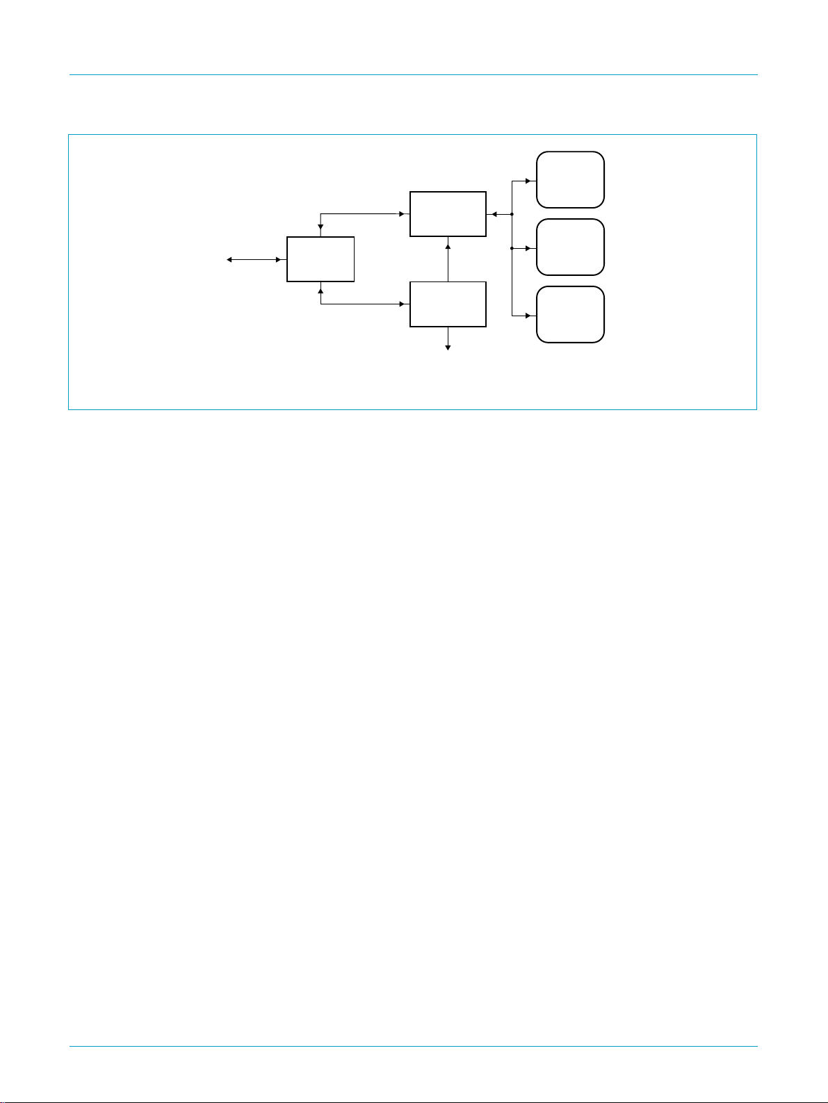
The Programmable Serial Interface Engine (PSIE) and Memory Management
Unit (MMU) is the heart of the USB protocol hardware (see Figure 5). It formats the
actual packets that are transferred to the USB and passes the incoming packets to
the right end-point buffers. These buffers are allocated as part of the USB RAM
space.
The microcontroller communicates via the I2C-bus with the PSIE-MMU. The I2C-bus
protocol distinguishes three register spaces. These spaces are addressed via
different commands. The command is sent to the command address.
Depending on the command it is sent to the PSIE-MMU and/or to the command
interpreter which configures the (de-)mux to open the path to the right register space.
Subsequent write/reads to/from the data address store or retrieve data from the
register space selected by the command.
8.8 ATX interface
The SAA8115HL contains an analog bus driver, called the ATX. It incorporates a
differential and two single-ended receivers and a differential transmitter.
The interface to the bus consists of a differential data pair (ATXDM and ATXDP).
9397 750 07395
Product specification Rev. 04 — 10 August 2000 12 of 51
© Philips Electronics N.V. 2000. All rights reserved.
Philips Semiconductors
to/from
microcontroller
PI_Address + 0X
I2C-BUS
INTERFACE
SAA8115HL
Digital camera USB interface
PSIE-MMU
REGISTER
SPACE
(DE)MUX
SET MODE
REGISTER
SPACE
Fig 5. I2C-bus interface and register map.
8.9 Audio
The SAA8115HL contains a microphone supply and an amplifier circuit composed of
two stages: a Low Noise Amplifier (LNA) and a variable gain amplifier. The LNA has a
fixed gain of 26 dB while the variable gain amplifier can be programmed
between 0 and 30 dB by steps of 2 dB. The gain control can be done via either the
SNERT interface or the I2C-bus interface (see Table 60). The serial interface must be
first selected using bit SIS (see Table 60). The frequency transfer characteristic of the
audio path must be controlled via external high-pass or low-pass filters.
The PLL converts the 48 MHz to 256fs(fs= audio sample frequency). There are three
modes for the PLL to achieve the sample frequencies of 48, 44.1 or 32 kHz
(see Table 5).
The bitstream ADC samples the audio signal. It runs at an oversample rate of
256 times the base sample rate. In the application, the bitstream can be converted to
parallel 16-bit samples. This conversion is programmable with respect to the effective
sample frequency (dropping sample results in a lower effective sample frequency)
and sample resolution. As a result the effective sample rate can be determined.
PI_Address + 10
COMMAND
INTERPRETER
to
PSIE-MMU
NON USB
AND
VIDEO FIFO
REGISTERS
FCE432
9397 750 07395
Product specification Rev. 04 — 10 August 2000 13 of 51
© Philips Electronics N.V. 2000. All rights reserved.

Philips Semiconductors
Table 5: ADC clock frequencies and sample frequencies
Clock
(MHz)
8.1920 1 32 4.096
11.2996 1 44.1 5.6448
12.2880 1 48 6.144
[1] Not supported.
SAA8115HL
Digital camera USB interface
Dividing
number
2 16 2.048
4 8 1.042
8
2 22.05 2.8224
4 11.025 1.4112
8 5.5125 0.7056
2 24 3.072
4 12 1.536
8 6 0.768
Sample
frequency
(kHz)
[1] [1]
ADC clock
(MHz)
8.10 Sensor pulse pattern generator
The SAA8115HL incorporates a Pulse Pattern Generator (PPG) function. The PPG
can be used for medium resolution PAL, CIF and VGA CCD-sensors (see Table 6).
Depending on the sensor type, an external inverter driver should be required to
convert the 3.3 V pulses into a voltage suitable for the used CCD-sensor.
The active video size is 512 × 288 for medium resolution PAL, 352 × 288 for CIF and
640 × 480 for VGA. The total H × V size are 685 × 292 for medium resolution PAL/CIF
and 823 × 486 for VGA. It should be noted that additional HD pulses are added
during the vertical blanking interval to reach a total of 312 lines in PAL and CIF modes
and 525 lines in VGA mode as required by the SAA8112HL.
A high level of flexibility is available for the PPG thanks to 19 internal registers (see
Section 9.1.3).
Table 6: Typical SAA8115HL compatible sensors
Sensor type Brand Part number
VGA Sony ICX098AK
Panasonic MN3777PP and MN37771PT
Sharp LZ24BP
Medium resolution PAL Sony ICX054, ICX086 and ICX206
Panasonic MN37210FP
Sharp LZ2423B and LZ2423H
Toshiba TCD5391AP
CIF Sharp LZ244D and LZ2547
Other sensors all the sensors fully compatible with the above mentioned sensors
9397 750 07395
Product specification Rev. 04 — 10 August 2000 14 of 51
© Philips Electronics N.V. 2000. All rights reserved.

Philips Semiconductors
8.11 Power management
USB requires the device to switch power states. The SAA8115HL contains a power
management module since the complete camera may not consume more than
500 µA during the power state called SUSPEND. This requires that even the crystal
oscillator must be switched off. The SAA8115HL is not functional except for some
logic that enables the IC to wake-up the camera. After wake-up of the SAA8115HL
first the clock to the microcontroller is generated and thereafter an interrupt is
generated to wake-up the microcontroller.Therefore the clock of the microcontroller is
generated by the SAA8115HL.
The power management module also sets a flag in register SET_MODE_AND_READ
(PSIE_MMU_STATUS).After a reset the microcontroller should check this register via
the I2C-bus and find the cause of the wake-up.Different causes may require different
start-up routines.
The internal video processing core uses another supply domain which can be
switched off during SUSPEND mode.
The PPG is switched off by setting PPG_RESUME_MODE (0x08) and resetting
PAL_VGA (0x09).
SAA8115HL
Digital camera USB interface
In non CIF modes the power consumption is reduced by resetting
COMPRESSION_MODE (0x2F) and COMPRESSION_CLOCK (0x09).
The SAA8115HL has the feature to autonomously wake-up from SUSPEND mode,
but requires microcontroller interference before going in SUSPEND mode (via the
signal on pin SUSPREADYNOT).
Since the main oscillator of the SAA8115HL is switched off during SUSPEND mode,
precautions are needed to avoid undefined states when the clock is switched on. This
is ensured via the pins CLOCKON and TRC. Pin CLOCKON goes HIGH as soon as
the main oscillator is switched on. The oscillator will need some time to make a stable
48 MHz signal. However, the clock is only passed through to other parts of the
SAA8115HL when the level on pin TRC reaches a certain threshold. The time
needed to reach the threshold can be trimmed with an external RC circuit.
8.12 Power supply
A power supply regulator is integrated in the device. This DC-to-DC converter
transforms the USB supply voltage (range from 4.0 to 5.5 V) into a stable 5 V supply
voltage. This power domain is switchable. The power circuit also generates a reset
signal when the external 3.3 V supply voltage is stable and in range.
9397 750 07395
Product specification Rev. 04 — 10 August 2000 15 of 51
© Philips Electronics N.V. 2000. All rights reserved.

Philips Semiconductors
9. Control register description
This specification gives an overview of all registers.
9.1 SNERT (UART)
The SAA8115HL is partly controlled via SNERT. The frame rate converter, the
SDRAM interface, the video formatter, the compression engine, the PPG, the SMP
and the audio functions are controlled via SNERT. This SNERT interface works
independently from the frame rate and can always be operated in the full frequency
range.
Via SNERT the following registers are accessible (see Table 7).
Table 7: SNERT write registers SAA8115HL
Address Function
00 write register soft reset (see Table 8)
01 to 05 write registers Frame Rate Converter (FRC) including the SDRAM interface
06 and 07 reserved
08 to 1A write registers Pulse Pattern Generator (PPG)
1B to 1F reserved
20 to 38 write registers video formatter and compression engine
39 to 3C reserved
3D and 3E write registers Switch Mode Power (SMP)
3F write register audio variable gain amplifier
SAA8115HL
Digital camera USB interface
9.1.1 General register
Table 8: Detailed description of SNERT general register 0x00
Bit SNERT register 00: SOFT_RESET
7 6 5 4 3 2 1 0 Parameter
XXXXX reserved
RESET_VP_C
1 compression engine in reset state
0 compression engine operating
RESET_VP_VF
1 formatter engine in reset state
0 formatter engine operating
RESET_FRC
1 frame rate converter engine in reset state (by default)
0 frame rate converter engine operating
9397 750 07395
Product specification Rev. 04 — 10 August 2000 16 of 51
© Philips Electronics N.V. 2000. All rights reserved.
 Loading...