

Philips SAA8113HL-C1, SAA8113HL-C101, SAA8113HL-C101-R5 Datasheet

DATA SH EET
Preliminary specification
File under Integrated Circuits, IC22
1999 Sep 27
INTEGRATED CIRCUITS
SAA8113HL
Digital PC-camera signal processor

1999 Sep 27 2
Philips Semiconductors Preliminary specification
Digital PC-camera signal processor SAA8113HL
CONTENTS
1 FEATURES
2 APPLICATIONS
3 GENERAL DESCRIPTION
4 ORDERING INFORMATION
5 QUICK REFERENCE DATA
6 BLOCK DIAGRAM
7 PINNING
8 FUNCTIONAL DESCRIPTION
8.1 Black offset preprocessing
8.2 Y, CRand CB separation
8.3 RGB processing
8.4 Y processing
8.5 RGB to UV conversion
8.6 UV processing
8.7 Display function
8.8 Analog output processing
8.9 Measurement engine
8.10 VH reference and window timing and control
8.11 Pulse pattern generator
8.12 Miscellaneous functions
8.13 Mode control
8.14 Microcontroller
8.15 Audio amplifier
8.16 I2C-bus interface
9 LIMITING VALUES
10 THERMAL CHARACTERISTICS
11 OPERATING CHARACTERISTICS
12 ELECTRICAL CHARACTERISTICS
13 APPLICATION INFORMATION
14 PACKAGE OUTLINE
15 SOLDERING
15.1 Introduction to soldering surface mount
packages
15.2 Reflow soldering
15.3 Wave soldering
15.4 Manual soldering
15.5 Suitability of surface mount IC packages for
wave and reflow soldering methods
16 DEFINITIONS
17 LIFE SUPPORT APPLICATIONS
18 PURCHASE OF PHILIPS I2C COMPONENTS

1999 Sep 27 3
Philips Semiconductors Preliminary specification
Digital PC-camera signal processor SAA8113HL
1 FEATURES
• High precision digital processing with 10-bit input
• Medium resolution complementary mosaic CCD
sensors PAL or NTSC (interlaced mode only)
• Internal PPG, dedicated to SHARP, TOSHIBA and
PANASONIC sensors
• Integrated microcontroller (80C51) for control loops
Auto Optical Black (AOB), Auto White Balance (AWB)
and Auto Exposure (AE)
• Black offset preprocessing
• RGB separation
• RGB processing (colour correction matrix,
programmable knee and gamma)
• Separate Y-processing (saturation concealment,
programmable knee and gamma)
• RGB to UV conversion (includingdown-sampling filters)
• Noise reduction in Y and UV
• Display function for system evaluation
• Analogoutputprocessing,includingPAL/NTSCencoder
and 9-bit Video Digital-to-Analog Converter (VDAC)
• Measurement engine (prepared for AE and AWB
features)
• Miscellaneous functions, e.g. power management, 7-bit
Control DAC (CDAC) serial interface with preprocessing
• VH reference and window timing for internal use
• Master I2C-bus interface for communication with an
external EEPROM (containing the default settings)
• Slave I2C-bus interface for communication with an
external microcontroller
• Parallel interface for communication with an external
EPROM (for ROM code debugging)
• Integrated audio amplifier.
2 APPLICATIONS
• Low-cost desktop video applications
• Videophone systems.
3 GENERAL DESCRIPTION
The SAA8113HL is a 2nd generation camera Digital
Signal Processor (DSP) designed for low-cost DTV
applications. It integrates the DSP core, the Pulse Pattern
Generator (PPG), the 80C51 microcontroller and the
VDAC in one IC. It is the successor of the SAA8110G,
dedicated to analog output cameras.
The SAA8113HL must be applied together with an analog
front-end that includes a Correlated Double Sampling
(CDS), an Automatic Gain Control (AGC) and an
Analog-to-Digital Converter (ADC). This may be the
TDA8786 or the TDA8784.
The PPG generates the timing pulses to drive medium
resolution PAL/NTSC complementary mosaic CCD
sensors (512 × 492 NTSC and 512 × 582 PAL).
The input of the DSP is 10 bits with a maximum pixel
frequency equal to 9.66 MHz. The DSP core processes
this sensor signal to a standard video output signal. The
SAA8113HL output is an analog CVBS video signal.
The microcontroller provides the settings for the IC
registers from EEPROM at power-up or reset and controls
the AWB, AE and AOB loops. It also provides a hardware
I2C-businterface,sothemicrocontrollercanbe used as an
I2C-bus slave. The software code is embedded in an
internalROM but it is also possibleto use a combined data
and address bus, connected to an external program
EPROM.
A built-in power management function allows the power
dissipation to be optimized.
4 ORDERING INFORMATION
TYPE
NUMBER
PACKAGE
NAME DESCRIPTION VERSION
SAA8113HL LQFP100 plastic low profile quad flat package; 100 leads;
body 14 × 14 × 1.4 mm
SOT407-1
1999 Sep 27 4
Philips Semiconductors Preliminary specification
Digital PC-camera signal processor SAA8113HL
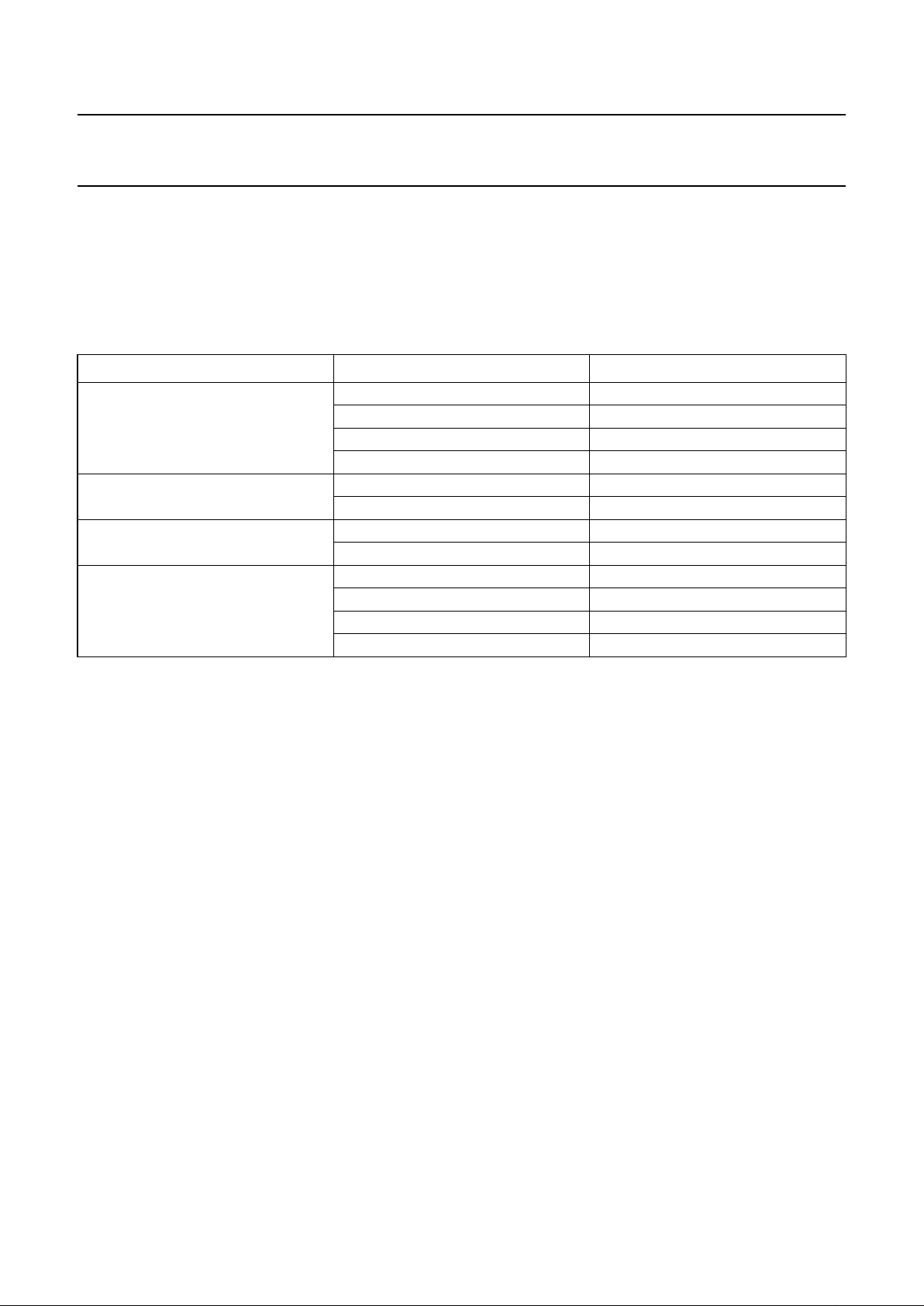
5 QUICK REFERENCE DATA
Measured over full voltage and temperature range.
Note
1. This concerns pins SCL and SDA.
SYMBOL PARAMETER CONDITIONS MIN. TYP. MAX. UNIT
V
DDD
digital supply voltage 3.0 3.3 3.6 V
V
DDA
analog supply voltage 3.0 3.3 3.6 V
I
DD(tot)
total supply current V
DDD
= 3.3 V − 60 − mA
V
I
input voltage 3.0V<V
DDD
< 3.6 V low-voltage TTL compatible V
note 1 5 V tolerant, TTL compatible V
V
O
output voltage 3.0V<V
DDD
< 3.6 V low-voltage TTL compatible V
note 1 5 V tolerant, TTL compatible V
f
clk
clock frequency input − 38 − MHz
δ duty factor of f
clk
− 50 − %
P
tot
total power dissipation T
amb
=25°C − 200 250 mW
T
stg
storage temperature −55 − +150 °C
T
amb
ambient temperature 0 25 70 °C
T
j
junction temperature T
amb
=70°C −40 − +125 °C
1999 Sep 27 5
Philips Semiconductors Preliminary specification
Digital PC-camera signal processor SAA8113HL
This text is here in white to force landscape pages to be rotated correctly when browsing through the pdf in the Acrobat reader.This text is here in
_white to force landscape pages to be rotated correctly when browsing through the pdf in the Acrobat reader.This text is here inThis text is here in
white to force landscape pages to be rotated correctly when browsing through the pdf in the Acrobat reader. white to force landscape pages to be ...
6 BLOCK DIAGRAM
b
ook, full pagewidth
FCE312
MICRO-
CONTROLLER
80C51
SAA8113HL
INTERNAL
MICRO-
CONTROLLER
INTERFACE
ANALOG
OUTPUT
(PRE-
PROCESSING)
PAL/NTSC
ENCODER
P1
P2
AUDIO BUFFER
VDAC
P0
P4
P3
5, 6, 7, 8
11
SDAE
15
SDA
14
SCL
DISPLAY
UV
PROCESSING
RGB
TO
UV
RGB
PROCESSING
Y
AND
CR, C
B
SEPARATION
OFFSET
PRE-
PROCESSING
Y
PROCESSING
10
SCLE
85 to 94
MODE
CONTROL
AND
CLOCK
GENERATOR
1 to 3
28 3 9 2 2
8
7
4
24638
3
10
62
63
59
58
50
ALE
49 to 42
P0.7 to P0.0
39 to 33
AD14 to AD8
KNOB3
to
KNOB0
CCD9
to
CCD0
M2 to M0
32
PSEN
22
18
27
26, 28
29
V
DDA4
24, 2555, 96
V
DDD1,
V
DDD2
13, 17, 23,
40, 57, 64, 71, 83
54, 56, 95 12, 19, 20, 21,
41, 60, 61, 72, 82
AGND5,
AGND6
MICIAB,
V
COMAB
V
DDA1 to VDDA3
,
V
DDA5
to
V
DDA9 DGND1 to DGND3
AGND1 to AGND4,
AGND7 to AGND11
OUTAB
XOSC
XIN
XOUT
CDACOUT
RBIASCDAC
MISCELLANEOUS
FUNCTIONS
PPG
SENSOR/PREPROCESSOR TIMING AND CONTROL
VH
REFERENCE
TIMING
MEASUREMENT ENGINE
CDAC
4 16, 53
KNOB4
9
RESET
52
EA
100, 99,
98, 97,
84, 51,
30, 31
SDATA,
SCLK,
STROBE,
STDBY,
SMP,
LED,
OUTBVEN,
OUTGAIN
65, 66,
67, 68,
69, 70
V1X,
VH1X,
V2X,
V3X,
VH3X,
V4X
75,
74, 76
FH1,
FH2,
FR
73
OFDX
79, 80,
77, 78
BCP,
DCP,
FS,
FCDS
81
T1,
INT1
CLK1
VDOBCVBS
DECREF
Fig.1 Block diagram.

1999 Sep 27 6
Philips Semiconductors Preliminary specification
Digital PC-camera signal processor SAA8113HL
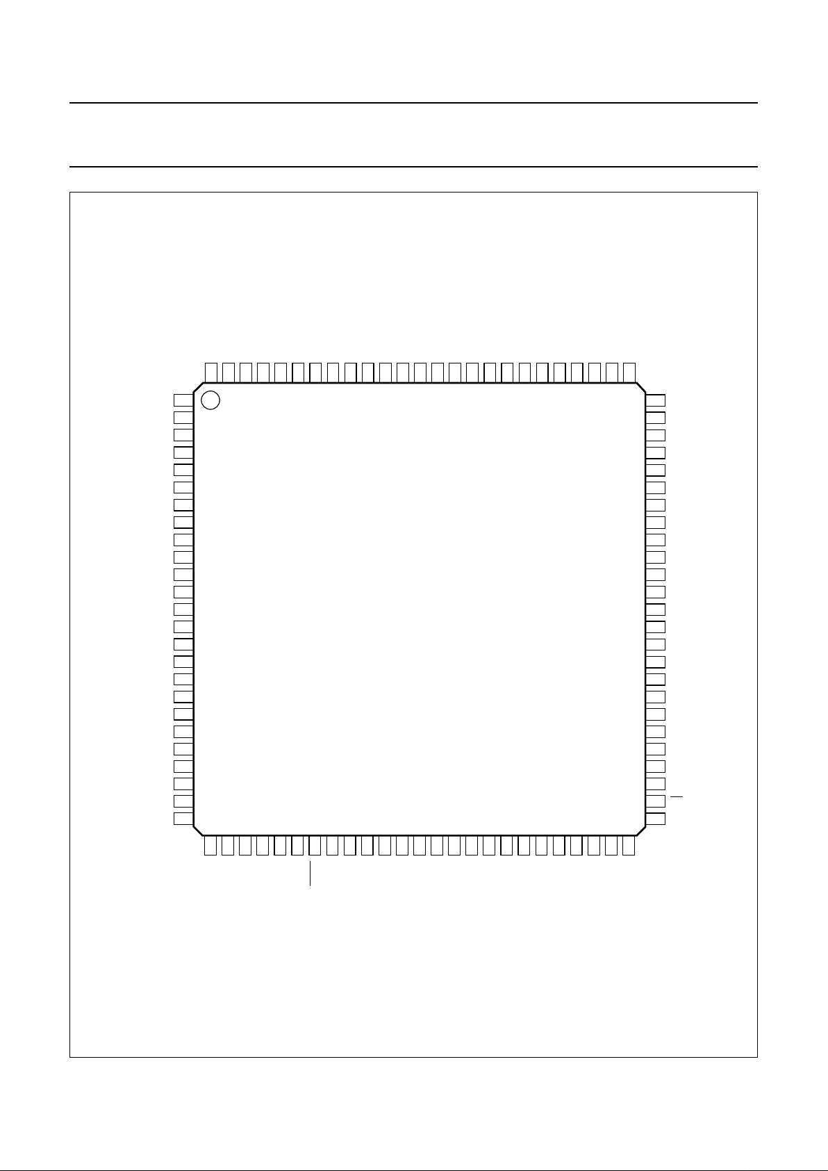
7 PINNING
SYMBOL PIN I/O DESCRIPTION
M2 1 I test mode control signal bit 2
M1 2 I test mode control signal bit 1
M0 3 I test mode control signal bit 0
KNOB4 4 I input connected to DSP core
KNOB3 5 I/O I/O connected to internal 80C51
KNOB2 6 I/O I/O connected to internal 80C51
KNOB1 7 I/O I/O connected to internal 80C51
KNOB0 8 I/O I/O connected to internal 80C51
RESET 9 I Power-on reset
SCLE 10 O master I
2
C-bus clock output to control EEPROM
SDAE 11 I/O master I
2
C-bus data I/O to control EEPROM
AGND1 12 I analog ground 1 for output buffers
V
DDA1
13 I analog supply voltage 1 for output buffers
SCL 14 I slave I
2
C-bus clock input
SDA 15 I/O slave I
2
C-bus data I/O
T1 16 I Timer 1 for internal 80C51
V
DDA2
17 I analog supply voltage 2 for DAC output buffer
VDOBCVBS 18 O VDAC output buffer for CVBS signal
AGND2 19 I analog ground 2 for DAC output buffer
AGND3 20 I analog ground 3 for analog DAC core and band gap (connected to substrate)
AGND4 21 I analog ground 4 for analog DAC core and band gap (not connected to substrate)
DECREF 22 O decoupled pin for reference voltage HIGH
V
DDA3
23 I analog supply voltage 3 for analog DAC core and band gap
MICIAB 24 I microphone input audio buffer
V
COMAB
25 I common voltage for audio buffer
AGND5 26 I analog ground 5 for audio buffer (not connected to substrate)
OUTAB 27 O output audio buffer
AGND6 28 I analog ground 6 for audio buffer (connected to substrate)
V
DDA4
29 I analog supply voltage 4 for audio buffer
OUTBVEN 30 O output to enable the bias voltage of the microphone for the audio buffer
OUTGAIN 31 O output to control the gain factor of an external audio buffer
PSEN 32 O program store enable; read strobe for external program memory (active LOW)
AD8 33 O address bit 8 for external program memory (PROM)
AD9 34 O address bit 9 for external program memory (PROM)
AD10 35 O address bit 10 for external program memory (PROM)
AD11 36 O address bit 11 for external program memory (PROM)
AD12 37 O address bit 12 for external program memory (PROM)
AD13 38 O address bit 13 for external program memory (PROM)
AD14 39 O address bit 14 for external program memory (PROM)
V
DDA5
40 I analog supply voltage 5 for output buffers
1999 Sep 27 7
Philips Semiconductors Preliminary specification
Digital PC-camera signal processor SAA8113HL
AGND7 41 I analog ground 7 for output buffers
P0.0 42 I/O port 0 bidirectional bit 0 for external program memory data I/O (PROM)
P0.1 43 I/O port 0 bidirectional bit 1 for external program memory data I/O (PROM)
P0.2 44 I/O port 0 bidirectional bit 2 for external program memory data I/O (PROM)
P0.3 45 I/O port 0 bidirectional bit 3 for external program memory data I/O (PROM)
P0.4 46 I/O port 0 bidirectional bit 4 for external program memory data I/O (PROM)
P0.5 47 I/O port 0 bidirectional bit 5 for external program memory data I/O (PROM)
P0.6 48 I/O port 0 bidirectional bit 6 for external program memory data I/O (PROM)
P0.7 49 I/O port 0 bidirectional bit 7 for external program memory data I/O (PROM)
ALE 50 O address latch enable pulse for external latch
LED 51 O output to drive LED
EA 52 I external access select bit for internal 80C51 (active LOW)
INT1 53 I interrupt 1 for internal 80C51
DGND1 54 I digital ground 1 for input buffers, predrivers and the digital core
V
DDD1
55 I digital supply voltage 1 for input buffers, predrivers and the digital core
DGND2 56 I digital ground 2 for input buffers, predrivers and the digital core
V
DDA6
57 I analog supply voltage 6 for CDAC
RBIASCDAC 58 O bias resistor for CDAC
CDACOUT 59 O output CDAC
AGND8 60 I analog ground 8 for CDAC
AGND9 61 I analog ground 9 for 38 MHz (fundamental) crystal oscillator
XIN 62 I oscillator input
XOUT 63 O oscillator output
V
DDA7
64 I analog supply voltage 7 for 38 MHz (fundamental) crystal oscillator
V1X 65 O vertical CCD transfer pulse 1X
VH1X 66 O vertical CCD load pulse H1X
V2X 67 O vertical CCD transfer pulse 2X
V3X 68 O vertical CCD transfer pulse 3X
VH3X 69 O vertical CCD load pulse H3X
V4X 70 O vertical CCD transfer pulse 4X
V
DDA8
71 I analog supply voltage 8 for output buffers
AGND10 72 I analog ground 10 for output buffers
OFDX 73 O overflow drain pulse for shutter control
FH2 74 O horizontal CCD transfer pulse F2
FH1 75 O horizontal CCD transfer pulse F1
FR 76 O CCD output amplifier reset pulse (TDA8786 or TDA8784)
FS 77 O CCD output level sample and hold pulse (TDA8786 or TDA8784)
FCDS 78 O reference level sample and hold pulse (TDA8786 or TDA8784)
BCP 79 O black pixel clamp pulse (TDA8786 or TDA8784)
DCP 80 O dummy pixel clamp pulse (TDA8786 or TDA8784)
CLK1 81 O pixel clock to preprocessor (TDA8786 or TDA8784)
SYMBOL PIN I/O DESCRIPTION
1999 Sep 27 8
Philips Semiconductors Preliminary specification
Digital PC-camera signal processor SAA8113HL
AGND11 82 I analog ground 11 for output buffers
V
DDA9
83 I analog supply voltage 9 for output buffers
SMP 84 O switch mode pulse for DC-to-DC power supply
CCD9 85 I (preprocessed) AD-converted CCD signal bit 9
CCD8 86 I (preprocessed) AD-converted CCD signal bit 8
CCD7 87 I (preprocessed) AD-converted CCD signal bit 7
CCD6 88 I (preprocessed) AD-converted CCD signal bit 6
CCD5 89 I (preprocessed) AD-converted CCD signal bit 5
CCD4 90 I (preprocessed) AD-converted CCD signal bit 4
CCD3 91 I (preprocessed) AD-converted CCD signal bit 3
CCD2 92 I (preprocessed) AD-converted CCD signal bit 2
CCD1 93 I (preprocessed) AD-converted CCD signal bit 1
CCD0 94 I (preprocessed) AD-converted CCD signal bit 0
DGND3 95 I digital ground 3 for input buffers, predrivers and the digital core
V
DDD2
96 I digital supply voltage 2 for input buffers, predrivers and the digital core
STDBY 97 O standby control output to TDA8786 or TDA8784
STROBE 98 O strobe to TDA8786 or TDA8784
SCLK 99 O serial clock to TDA8786 or TDA8784
SDATA 100 O serial data to TDA8786 or TDA8784
SYMBOL PIN I/O DESCRIPTION
1999 Sep 27 9
Philips Semiconductors Preliminary specification
Digital PC-camera signal processor SAA8113HL
handbook, full pagewidth
75
74
73
72
71
70
69
68
67
66
65
64
63
62
61
60
59
58
57
56
55
54
53
52
51
8079787776
DCP
BCP
FCDSFSFR
FH1
FH2
OFDX
AGND10
V
DDA8
V4X
VH3X
V3X
V2X
VH1X
V1X
V
DDA7
XOUT
XIN
AGND9
AGND8
CDACOUT
RBIASCDAC
V
DDA6
DGND2
V
DDD1
DGND1
INT1
EA
LED
M2
M1
M0
KNOB4
KNOB3
KNOB2
KNOB1
KNOB0
RESET
SCLE
SDAE
AGND1
V
DDA1
SCL
SDA
T1
V
DDA2
VDOBCVBS
AGND2
AGND3
AGND4
DECREF
V
DDA3
MICIAB
V
COMAB
SDATA
SCLK
STROBE
STDBY
V
DDD2
DGND3
CCD0
CCD1
CCD2
CCD3
CCD4
CCD5
CCD6
CCD7
CCD8
CCD9
SMP
V
DDA9
AGND11
CLK1
OUTGAIN
AD8
AD9
AD10
AD11
AD12
AD13
AD14
V
DDA5
AGND7
P0.0
P0.1
P0.2
P0.3
P0.4
P0.5
P0.6
P0.7
ALE
AGND5
OUTAB
AGND6
V
DDA4
OUTBVEN
30
29
28
27
26
25
24
23
22
21
20
19
18
17
16
15
14
13
12
11
10
9
8
7
6
5
4
3
2
1
100
99989796959493929190898887868584838281
31323334353637383940414243444546474849
50
SAA8113HL
PSEN
FCE313
Fig.2 Pin configuration.
1999 Sep 27 10
Philips Semiconductors Preliminary specification
Digital PC-camera signal processor SAA8113HL
8 FUNCTIONAL DESCRIPTION
8.1 Black offset preprocessing
The CCD signal contains additional pixels outside the
active window, which are used to measure the reference
black level. These pixels are located in the optical black
window, whose position can be set through the serial
interface. The optical black level can be adjusted by the
microcontrollerinorderto proceed rapidly. In this case, the
microcontroller directly adjusts the analog preprocessing
clamp included in the TDA8786 or TDA8784 and takes
advantage of the full code range. Otherwise, the black
level is fixed by settings that are downloaded through the
serial interface.
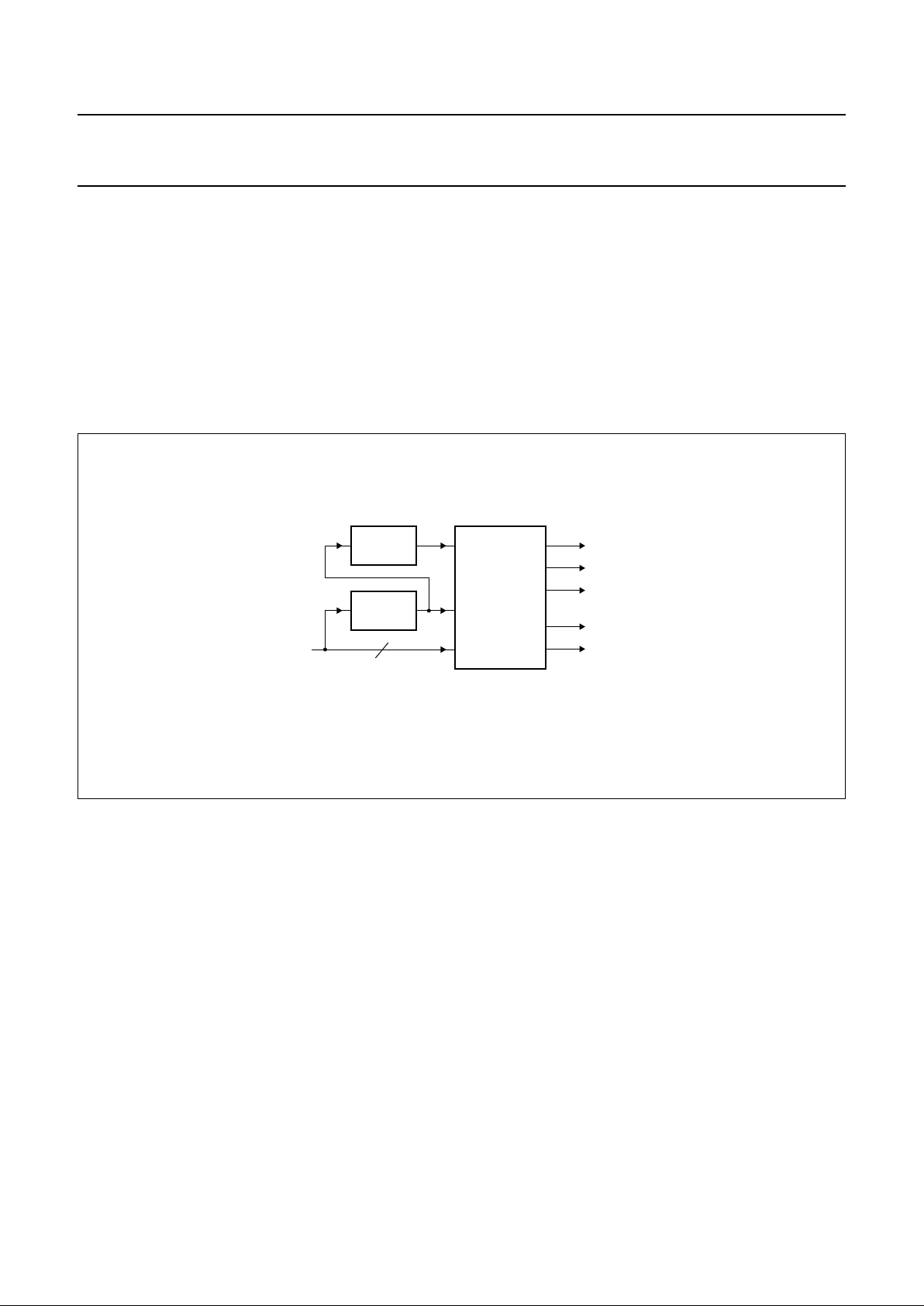
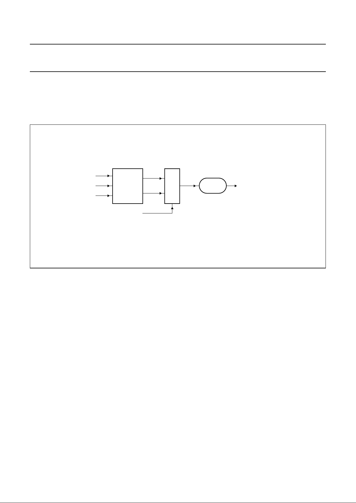
8.2 Y, CRand CB separation
For each pixel value, this block (see Fig.3) generates the
three components: the luminance signal Y and the two
colour signals C
R
(2R − G) and CB(2B − G). Two line
memories are required for this function. This block also
provides vertical contour and white clip information.
handbook, full pagewidth
FCE314
10
CCD inputs
Y
C
R
C
B
white clip
Y
vertical contour
LINE
MEMORY
LINE
MEMORY
RGB
COLOUR
SEPARATION
Fig.3 Y, CRand CB separation diagram.
1999 Sep 27 11
Philips Semiconductors Preliminary specification
Digital PC-camera signal processor SAA8113HL
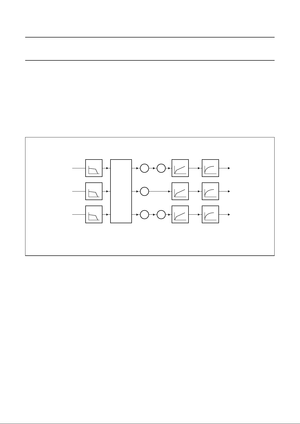
8.3 RGB processing
The RGB processing (see Fig.4)includes several features:
• Colour space matrix to handle different types of colour
sensors. The result is an optimum colour reproduction
through the minimization of colour errors. The default
matrixcoefficients(positiveornegative)canbeadjusted
through an external interface.
• Separate and adjustable black offsets for
R, G and B signals.
• Separate gain controls for R and B signals dedicated to
white balance control. The colour temperature can be
adjusted independently of the colour matrix.
• Knee function (compression factor and knee point are
adjustable).
• Adjustable gamma function to compensate for the
non-linearity of display devices.
The RGB path has a reduced bandwidth (less than
1 MHz), which is required for CVBS output.
handbook, full pagewidth
FCE315
KNEE
Y
R
R
gain
R
black
LPF GAMMA
×
+
KNEE
COLOUR
MATRIX
C
R
G
G
black
LPF GAMMA
+
KNEE
C
B
B
B
gain
B
black
LPF GAMMA
×
+
Fig.4 RGB processing diagram.
1999 Sep 27 12
Philips Semiconductors Preliminary specification
Digital PC-camera signal processor SAA8113HL
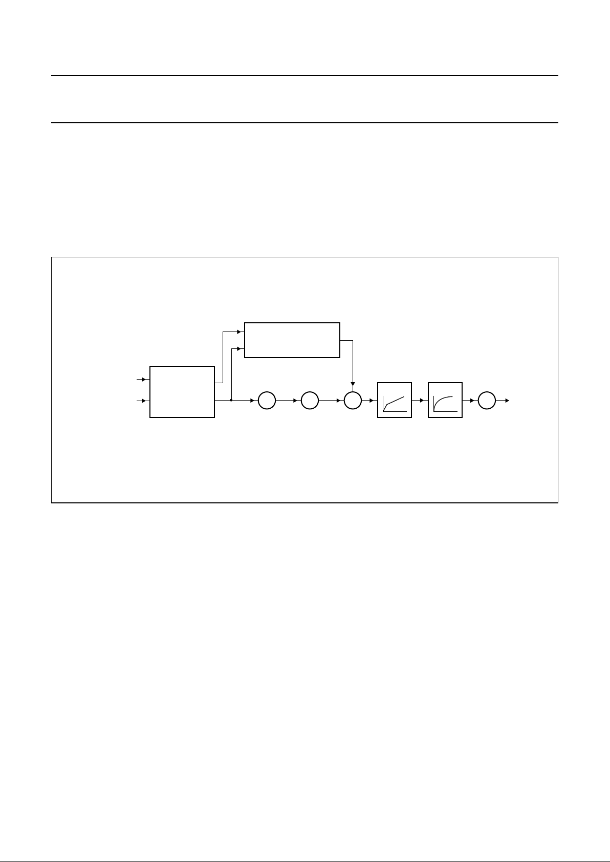
8.4 Y processing
The separate Y processing (see Fig.5) includes the
following features:
• Saturation concealment to reduce the typical saturation
distortion
• Contour processing to improve picture sharpness
• Noise reduction
• Black offset
• Pre-gaincontroltoadjust the Y signal with respect to the
gamma range
• Knee function (compression factor and knee point are
adjustable)
• Adjustable gamma function
• Gain control.
handbook, full pagewidth
FCE316
KNEE
SATURATION
CONCEALMENT
Y
Y
Y
pre-gain
Y
black
Y
vertical contour
CONTOUR PROCESSING
AND
NOISE REDUCTION
GAMMA
×
Y
gain
×
+ +
Fig.5 Y processing diagram.
8.5 RGB to UV conversion
After R, G and B processing, the data path is converted to
U and V signals (see Fig.1). As a result of the reduced
bandwidth, the Y signal is only used as an input for control
loop purposes (measurement engine).
8.6 UV processing
The chrominance processing consists of a noise reduction
by coring and the UV gain control.
8.7 Display function
As an optional feature and for software debugging, it is
possible to visualize:
• Eight display bars (assigned via the microcontroller)
• Several measurement engine inputs.
1999 Sep 27 13
Philips Semiconductors Preliminary specification
Digital PC-camera signal processor SAA8113HL
8.8 Analog output processing
The analog output processing (see Fig.6) contains a
PAL/NTSC encoder to transform the YUV data path to the
CVBS output. The YUV input signals are up-sampled to
twice the pixel clock and digitally prefiltered to keep the
external analog filter simple. The block also contains an
adjustable luminance clipper.
handbook, full pagewidth
FCE317
U
Y
V
sync, blank, scaling, levels
Y
VDOBCVBS
C
PAL/NTSC
ENCODER
MIX
VDAC
Fig.6 Analog output processing.
8.9 Measurement engine
The measurement engine performs data measurements
on a field basis to get inputs for the AE and AWB control
loops of the microcontroller. Up to 16 programmable
windows can be used for the measurement. There are two
down-samplers to prepare the data for two separate
accumulators. It is possible to proceed with eight different
measurements per field (odd and even fields separately).
An internal RAM workspace is used for data handling
operation.
8.10 VH reference and window timing and control
This block generates internal control signals for different
purposes:
• Vertical, horizontal and field references (VD,HDand FI)
for PAL or NTSC sensors
• Specification of the active window and the optical black
window
• Specification of the measurement window grid with
respect to the active window
• Specification of the vertical position of the display bars,
see Section 8.7.
Allthesespecifications can be controlled through the serial
interface.
1999 Sep 27 14
Philips Semiconductors Preliminary specification
Digital PC-camera signal processor SAA8113HL
8.11 Pulse pattern generator
The PPG generates timing pulses (Figs. 7 to 10) for
driving the CCD sensor (including the vertical driver) and
pulses for the preprocessor TDA8786 or TDA8784
(correlated double sampling and black clamping).
The PPG is dedicated to the medium resolution sensors
with complementary mosaic colour filters (512 × 492
NTSC and 512 × 582 PAL) described in Table 1.
Figs. 11 and 12 show the PPG outputs.
Table 1 Medium resolution CCD sensors driven by the internal PPG; note 1
Note
1. All sensors are used with the vertical driver: NEC µPD16510.
The PPG includes special features:
• A charge reset is possible in every active line during the horizontal line blanking and multiple times during the vertical
blanking
• A fast shutter interface is available.
BRAND FORMAT TYPE
SHARP PAL 1/4” LZ2423A
NTSC 1/4” LZ2413A
PAL 1/5” LZ2523
NTSC 1/5” LZ2513
TOSHIBA PAL 1/4” TCD5391AP
NTSC 1/4” TCD5381AP
SHARP low voltage PAL 1/4” LZ2425
NTSC 1/4” LZ2415
PANASONIC PAL 1/4” MN37210FP
PAL 1/4” MN37201FP
NTSC 1/4” MN37110FP
NTSC 1/4” MN37101FP
 Loading...