

Philips SAA8112HL-C100, SAA8112HL-C200, SAA8112HL-C201 Datasheet

DATA SH EET
Product specification
Supersedes data of 1999 Oct 28
File under Integrated Circuits, IC22
2000 Jan 18
INTEGRATED CIRCUITS
SAA8112HL
Digitalcamerasignalprocessorand
microcontroller

2000 Jan 18 2
Philips Semiconductors Product specification
Digital camera signal processor and
microcontroller
SAA8112HL
CONTENTS
1 FEATURES
2 APPLICATIONS
3 GENERAL DESCRIPTION
4 QUICK REFERENCE DATA
5 ORDERING INFORMATION
6 BLOCK DIAGRAM
7 PINNING
8 FUNCTIONAL DESCRIPTION
8.1 Synchronization and video windows
8.2 Optical black processing
8.3 Colour extractor
8.4 Colour matrix
8.4.1 RGB processing
8.5 YUV processing
8.5.1 Y processing
8.5.2 UV processing
8.6 Output formatter
8.7 Measurement Engine
8.8 Display features
8.9 Microcontroller
8.10 Mode control
8.11 SNERT (UART) interface - DSP registers
9 LIMITING VALUES
10 THERMAL CHARACTERISTICS
11 OPERATING CHARACTERISTICS
12 ELECTRICAL CHARACTERISTICS
13 APPLICATION INFORMATION
14 PACKAGE OUTLINE
15 SOLDERING
15.1 Introduction to soldering surface mount
packages
15.2 Reflow soldering
15.3 Wave soldering
15.4 Manual soldering
15.5 Suitability of surface mount IC packages for
wave and reflow soldering methods
16 DEFINITIONS
17 LIFE SUPPORT APPLICATIONS
18 PURCHASE OF PHILIPS I2C COMPONENTS

2000 Jan 18 3
Philips Semiconductors Product specification
Digital camera signal processor and
microcontroller
SAA8112HL
1 FEATURES
• High precision digital processing with 8- to 10-bit input
• Embedded microcontroller (80C51 core based) for
control loops Auto Optical Black (AOB), Auto White
Balance (AWB) and Auto Exposure (AE)
• Supports a large number of sensors
• RGB Bayer or mosaic (yellow, magenta, green and
cyan) colour processing
• Black and white processing without loss of resolution
• Compatible with interlaced or progressive modes
• Processes up to 800 active pixels per line
• Optical black processing
• Programmable colour matrix
• Programmable R, G and B offsets
• Programmable Knee and Gamma correction
• Programmable edge enhancement
• False colour detection and correction
• Y and UV adjustable coring filters
• Flexible Measurement Engine (ME) with up to 16
measurements per frame in 16 programmable windows
• Programmable measurement conditions on Y, U and V
• 8-bit YUV output with selectable formats:
– YUV 4:2:2 CCIR656 with signal embedded
synchronization codes (SAV/EAV)
– Selectable YUV output format 4 : 0 : 0, 4 :1:1,
4:2:2and4:4:4(according toIEEE-1394based
digital camera specification)
– Basic output window cutter and scaler.
• Programmable output clock for switched mode power
supply
• 3-wire/13-bitinterface for control of the TDA878X family
(CDS + AGS + 10-bit ADC).
2 APPLICATIONS
• PC camera
• Videophone
• Security camera
• Camcorder.
3 GENERAL DESCRIPTION
The SAA8112HL is a powerful and versatile 10-bit digital
processor for video cameras. It processes the digitized
sensor data and converts it to a high quality, multi-format
and YUV digital signal. In addition, the SAA8112HL
performs programmable statistical measurements on the
video stream allowing, for instance, a precise
measurement of the exposure or the white balance levels.
An 80C51 microcontroller derivative with five I/O ports,
I2C-bus, 512 bytes of RAM and 32 kbytes of program
memory is also embedded in the SAA8112HL.
The microcontroller is used in combination with the Digital
Signal Processing (DSP) measurement capabilities to
provideadvanced AE, AWB and AOB. The microcontroller
may also be used to control other devices in the camera,
for example a USB or a 1394 interface.
In the following description of the SAA8112HL, four main
functional blocks are given (see Fig.1):
• The DSP block
• The DSP ME block
• The microcontroller block
• Thetiming, interface and miscellaneous functions block.
2000 Jan 18 4
Philips Semiconductors Product specification
Digital camera signal processor and
microcontroller
SAA8112HL
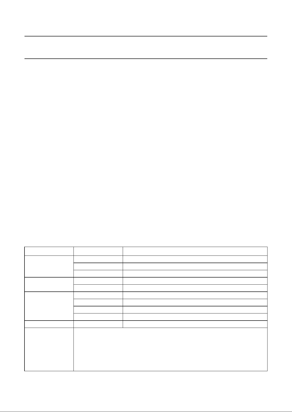
4 QUICK REFERENCE DATA
Measured over full voltage and temperature range: V
DDD
= 3.3 V ±10%; T
amb
= 0 to 70 °C; unless otherwise stated.
5 ORDERING INFORMATION
SYMBOL PARAMETER CONDITIONS MIN. TYP. MAX. UNIT
V
DDD
digital supply voltage 3.0 3.3 3.6 V
I
DDD(tot)
total supply current V
DDD
= 3.6 V
T
amb
=70°C
−−80 mA
V
I
input voltage 3.0V<V
DDD
< 3.6 V low voltage TTL
compatible
V
V
O
output voltage 3.0V<V
DDD
< 3.6 V low voltage TTL
compatible
V
f
clk(px)
pixel frequency 0 14.18 25 MHz
f
clk(µc)
microcontroller clock frequency 0 12 − MHz
P
tot
total power dissipation V
DDD
= 3.6 V
T
amb
=70°C
−−288 mW
T
stg
storage temperature −55 − +150 °C
T
amb
ambient temperature 0 25 70 °C
T
j
junction temperature T
amb
=70°C −−125 °C
TYPE
NUMBER
PACKAGE
NAME DESCRIPTION VERSION
SAA8112HL LQFP100 plastic low profile quad flat package; 100 leads;
body 14 × 14 × 1.4 mm
SOT407-1
2000 Jan 18 5
Philips Semiconductors Product specification
Digital camera signal processor and
microcontroller
SAA8112HL
This text is here in white to force landscape pages to be rotated correctly when browsing through the pdf in the Acrobat reader.This text is here in
_white to force landscape pages to be rotated correctly when browsing through the pdf in the Acrobat reader.This text is here inThis text is here in
white to force landscape pages to be rotatedcorrectly when browsing through thepdf in the Acrobat reader. whiteto force landscape pages tobe ...
6 BLOCK DIAGRAM
a
ndbook, full pagewidth
FCE338
SNERT INTERFACE
DIGOUTDISPLAY
RGB
to
YUV
MICRO-
CONTROLLER
80C51
P2
P3
P4
P0
P1
UV-PROCESSING
MEASUREMENT ENGINE
INTERNAL
WINDOW TIMING AND CONTROL
Y-PROCESSING
RGB
PROCESSING
RGB
SEPARATION
(incl. LMs)
VH
REFERENCE TIMING
OFFSET
PRE-
PROCESSING
MISCELLANEOUS
FUNCTIONS
49
PSEN
SDATA
SCLK
STROBE
SMP
17 to 19,
2
CCD9
to
CCD0
V
DDD1 to
V
DDD4
V
DD1 to
V
DD5
5 to 14
1, 3, 16, 68
29 to 33
5
P2.7 to P2.3
81 to 84
88 to 91
8
YUV7
to
YUV0
79,
77 to 75
4
LLC,
HREF,
VS,
PXQ
34 to 36
3
P2.2 to P2.0
20
P1.7/SDA
39 to 46
8
P0.7 to P0.0
10
4
78, 87, 94,
37, 47
5
DGND1 to
DGND4
GND1 to
GND5
100, 4, 15, 67
4
80, 86, 92,
38, 48
5
4
CLK1
CLK2
99, 93
2
M
DSPRST
85, 98
2
HD
VD
FI
95 to 97
3
50
ALE
21
P1.6/SCL
22 to 27
6
P1.5 to P1.0
3
69 to 71
UCCLK
UCM
UCRST
P3.7/RD
P3.6/WR
P3.5/T1
P3.4/T0
P3.3/INT1
P3.2/INT0
P3.1/TXD
P3.0/RXD
73
SNDA
2
72, 74
SNCL,
SNRES
28
8
59 to 66
P4.7
to
P4.0
2
51, 52
4
53 to 56
2
57, 58
SAA8112HL
EA
Fig.1 Block diagram.

2000 Jan 18 6
Philips Semiconductors Product specification
Digital camera signal processor and
microcontroller
SAA8112HL
7 PINNING
SYMBOL PIN
I/O
DESCRIPTION
V
DDD1
1 P digital supply voltage 1 for the DSP core (switchable supply domain)
SMP 2 O switched mode pulse for DC-to-DC power supply
V
DDD2
3 P digital supply voltage 2 for input buffers and predrivers
DGND2 4 P digital ground 2 for input buffers and predrivers and for the digital core
CCD9 5 I (preprocessed) AD-converted CCD; bit 9
CCD8 6 I (preprocessed) AD-converted CCD; bit 8
CCD7 7 I (preprocessed) AD-converted CCD; bit 7
CCD6 8 I (preprocessed) AD-converted CCD; bit 6
CCD5 9 I (preprocessed) AD-converted CCD; bit 5
CCD4 10 I (preprocessed) AD-converted CCD; bit 4
CCD3 11 I (preprocessed) AD-converted CCD; bit 3
CCD2 12 I (preprocessed) AD-converted CCD; bit 2
CCD1 13 I (preprocessed) AD-converted CCD; bit 1
CCD0 14 I (preprocessed) AD-converted CCD; bit 0
DGND3 15 P digital ground 3 for input buffers and predrivers and for the digital core
V
DDD3
16 P digital supply voltage 3 for input buffers and predrivers and for the 80C51 core
SCLK 17 O serial clock output to preprocessor
SDATA 18 O serial data output to preprocessor
STROBE 19 O strobe signal to preprocessor
P1.7/SDA 20 I/O Port 1 bidirectional; bit 7/slave I
2
C-bus data I/O
P1.6/SCL 21 I/O Port 1 bidirectional; bit 6/slave I
2
C-bus clock input
P1.5 22 I/O Port 1 bidirectional; bit 5
P1.4 23 I/O Port 1 bidirectional; bit 4
P1.3 24 I/O Port 1 bidirectional; bit 3
P1.2 25 I/O Port 1 bidirectional; bit 2
P1.1 26 I/O Port 1 bidirectional; bit 1
P1.0 27 I/O Port 1 bidirectional; bit 0
EA 28 I external access select - internal or external program memory (active LOW)
P2.7 29 O Port 2 output; bit 7
P2.6 30 O Port 2 output; bit 6
P2.5 31 O Port 2 output; bit 5
P2.4 32 O Port 2 output; bit 4
P2.3 33 O Port 2 output; bit 3
P2.2 34 I/O Port 2 bidirectional; bit 2
P2.1 35 I/O Port 2 bidirectional; bit 1
P2.0 36 I/O Port 2 bidirectional; bit 0
V
DD4
37 P supply voltage 4 for output buffers
GND4 38 P ground 4 for output buffers
P0.7 39 I/O Port 0 bidirectional; bit 7
P0.6 40 I/O Port 0 bidirectional; bit 6
2000 Jan 18 7
Philips Semiconductors Product specification
Digital camera signal processor and
microcontroller
SAA8112HL
P0.5 41 I/O Port 0 bidirectional; bit 5
P0.4 42 I/O Port 0 bidirectional; bit 4
P0.3 43 I/O Port 0 bidirectional; bit 3
P0.2 44 I/O Port 0 bidirectional; bit 2
P0.1 45 I/O Port 0 bidirectional; bit 1
P0.0 46 I/O Port 0 bidirectional; bit 0
V
DD5
47 P supply voltage 5 for output buffers
GND5 48 P ground 5 for output buffers
PSEN 49 O program store enable output for external memory (active LOW)
ALE 50 O address latch enable output for external latch
P3.7/
RD 51 O Port 3 output; bit 7/external data memory read output (active LOW)
P3.6/
WR 52 O Port 3 output; bit 6/external data memory write output (active LOW)
P3.5/T1 53 I Port 3 input; bit 5/Timer 1 external input
P3.4/T0 54 I Port 3 input; bit 4/Timer 0 external input
P3.3/INT1 55 I Port 3 input; bit 3/external interrupt 1
P3.2/INT0 56 I Port 3 input; bit 2/external interrupt 0
P3.1/TXD 57 I/O Port 3 input; bit 1/serial output port (UART)
P3.0/RXD 58 I/O Port 3 input; bit 0/serial input port (UART)
P4.7 59 I/O Port 4 bidirectional; bit 7
P4.6 60 I/O Port 4 bidirectional; bit 6
P4.5 61 I/O Port 4 bidirectional; bit 5
P4.4 62 I/O Port 4 bidirectional; bit 4
P4.3 63 I/O Port 4 bidirectional; bit 3
P4.2 64 I/O Port 4 bidirectional; bit 2
P4.1 65 I/O Port 4 bidirectional; bit 1
P4.0 66 I/O Port 4 bidirectional; bit 0
DGND4 67 P digital ground 4 for input buffers and predrivers and to the digital core
V
DDD4
68 P digital voltage4 for input buffers and predrivers and to the digital core
UCCLK 69 I clock for internal 80C51
UCM 70 I (test) mode control signal for internal 80C51
UCRST 71 I Power-on reset for internal 80C51
SNCL 72 I clock for DSP-SNERT interface (UART mode 0)
SNDA 73 I/O data I/O for DSP-SNERT interface (UART mode 0)
SNRES 74 I reset for DSP-SNERT interface (UART mode0)
PXQ 75 O pixel qualifier output for YUV-port
VS 76 O vertical synchronization output for YUV-port
HREF 77 O horizontal reference output for YUV-port
V
DD1
78 P supply voltage 1 for output buffers
LLC 79 O line-locked clock (delayed CLK2) for YUV-port
GND1 80 P ground 1 for output buffers
YUV7 81 O multiplexed YUV; bit 7
SYMBOL PIN
I/O
DESCRIPTION
2000 Jan 18 8
Philips Semiconductors Product specification
Digital camera signal processor and
microcontroller
SAA8112HL
YUV6 82 O multiplexed YUV; bit 6
YUV5 83 O multiplexed YUV; bit 5
YUV4 84 O multiplexed YUV; bit 4
M 85 I (test) mode control signal for DSP core
GND2 86 P ground 2 for output buffers
V
DD2
87 P supply voltage 2 for output buffers
YUV3 88 O multiplexed YUV; bit 3
YUV2 89 O multiplexed YUV; bit 2
YUV1 90 O multiplexed YUV; bit 1
YUV0 91 O multiplexed YUV; bit 0
GND3 92 P ground 3 for output buffers
CLK2 93 I double pixel clock input
V
DD3
94 P supply voltage 3 for output buffers
HD 95 I horizontal definition input
VD 96 I vertical definition input
FI 97 I field identification input
DSPRST 98 I Power-on reset for DSP
CLK1 99 I pixel clock input
DGND1 100 P digital ground 1 for input buffers and predrivers and for the digital core
SYMBOL PIN
I/O
DESCRIPTION

2000 Jan 18 9
Philips Semiconductors Product specification
Digital camera signal processor and
microcontroller
SAA8112HL
handbook, full pagewidth
75
74
73
72
71
70
69
68
67
66
65
64
63
62
61
60
59
58
57
56
55
54
53
52
51
8079787776
GND1
LLC
V
DD1
HREF
VS
PXQ
SNRES
SNDA
SNCL
UCRST
UCM
UCCLK
V
DDD4
DGND4
P4.0
P4.1
P4.2
P4.3
P4.4
P4.5
P4.6
P4.7
P3.0/RXD
P3.1/TXD
P3.2/INT0
P3.3/INT1
P3.4/T0
P3.5/T1
P3.6/WR
P3.7/RD
V
DDD1
SMP
V
DDD2
DGND2
CCD9
CCD8
CCD7
CCD6
CCD5
CCD4
CCD3
CCD2
CCD1
CCD0
DGND3
V
DDD3
SCLK
SDATA
STROBE
P1.7/SDA
P1.6/SCL
P1.5
P1.4
P1.3
P1.2
DGND1
CLK1
DSPRSTFIVDHDV
DD3
CLK2
GND3
YUV0
YUV1
YUV2
YUV3
V
DD2
GND2MYUV4
YUV5
YUV6
YUV7
P2.5
P2.4
P2.3
P2.2
P2.1
P2.0
V
DD4
GND4
P0.7
P0.6
P0.5
P0.4
P0.3
P0.2
P0.1
P0.0
V
DD5
GND5
ALE
P1.1
P1.0EAP2.7
P2.6
30
29
28
27
26
25
24
23
22
21
20
19
18
17
16
15
14
13
12
11
10
9
8
7
6
5
4
3
2
1
100
99989796959493929190898887868584838281
31323334353637383940414243444546474849
50
SAA8112HL
FCE339
PSEN
Fig.2 Pin configuration.
2000 Jan 18 10
Philips Semiconductors Product specification
Digital camera signal processor and
microcontroller
SAA8112HL
8 FUNCTIONAL DESCRIPTION
The SAA8112HL DSP block has a very high level of
programmability. The DSP alone uses 95 (8-bit) registers
(moreregistersareusedfortheME).TheSAA8112HLcan
accept 8- to 10-bit digital data from various sensors: CCD
or CMOS, progressive or interlaced, with or without colour
filters (see Table 1).
With B and W sensors, the full resolution is preserved.
The DSP registers are accessed through a serial interface
(UART).
8.1 Synchronization and video windows
To work properly, the SAA8112HL needs four or five input
synchronization signals:
• CLK1 (pixel clock)
• CLK2 (2 times the pixel clock)
• HD (horizontal reference)
• VD (vertical reference)
• FI (Field ID, useless for progressive scanning).
The incoming CCD data is sampled on the rising edge of
CLK1. The phase difference between CLK1 and CLK2
must be fixed.
The DSP working areas can be programmed and defined
with reference to the rising edges of HD and VD.
Several registers allow the definition of the optical black
window, the active video input window, the active video
output window and the measurement windows. With
interlaced applications, the windows are defined
separately for the odd and the even fields.
The number of active pixels per line is limited to 800,
although the total number of pixels can be higher. There is
no size limitation in the vertical direction.
8.2 Optical black processing
The first processing block of the SAA8112HL is a digital
clamp (denoted as OFFSET PRE_PROCESSING in
Fig.1). It is used to align the optical black level to zero or to
any arbitrary value.
When the digital clamp is set active, the average value of
the black is measured in the programmable optical black
window and then subtracted from the input signal.
A separate measurement is done for odd and even pixels
and for odd and even frames.
When the digital clamp is set inactive, it is possible to
subtract a fixed value from the incoming data stream.
A different value can be programmed for odd/even pixels,
odd/even fields and odd/even lines.
The optical black window has a fixed size of 16 pixels
(horizontally) by 128 (vertically), although the position of
this window is fully programmable.
Table 1 Typical SAA8112HL compatible sensors
SENSOR TYPE BRAND PART NUMBER
VGA SONY ICX084 and ICX098
PANASONIC MN3777
SHARP LZ24BP
HR SONY ICX058, ICX059, ICX068, ICX069, ICX208 and ICX209
SHARP LZ2453 and LZ2463
MR SONY ICX054, ICX086 and ICX206
SHARP LZ2413 and LZ2423
TOSHIBA TCM5391AP
PANASONIC MN37210FP
CIF SHARP LZ244D and LZ2547
Other sensors All sensors that fulfil the following criteria:
• B and W; complementary mosaic or RGB Bayer colour filter
• 8-, 9- or 10-bit input
• Up to 800 active pixels per line
• CMOS or CCD sensors
• Interlaced; progressive and non-interlaced sensors.

2000 Jan 18 11
Philips Semiconductors Product specification
Digital camera signal processor and
microcontroller
SAA8112HL
8.3 Colour extractor
The SAA8112HL colour extractor (denoted as RGB
SEPARATION in Fig.1) can be programmed to work with
both mosaic (yellow, magenta, green and cyan) and RGB
Bayer colour sensors.
With mosaic sensors, a combination (either sum or
subtraction) of consecutive pixels is used to extract a Y,
(2R-G) and (2B-G) triplet for all pixels.
WithRGB Bayer sensors, an RGBtriplet is interpolated for
every pixel on a 3 × 3 neighbourhood matrix.
With B and W sensors, the colour extractor can be
disabled, thus maintaining the full sensor resolution.
Edges and video level information (white clip) are
extracted at this stage (see Fig.3).
handbook, full pagewidth
FCE340
LINE
MEMORY
LINE
MEMORY
R
G
B
10
CCD inputs
White clip
RGB
COLOUR
SEPARATION
Edges
Fig.3 RGB separation diagram.

2000 Jan 18 12
Philips Semiconductors Product specification
Digital camera signal processor and
microcontroller
SAA8112HL
8.4 Colour matrix
A programmable 3 × 3 colour matrix (see Fig.4) is used to
convert the extracted colour information, either Y, (2R-G),
(2B-G) or R, G and B from the sensor colour space into a
standard RGB colour space.
With B and W sensors, a unity matrix is used.
8.4.1 RGB PROCESSING
At the colour matrix output, the video signal is in RGB
format. The following processing is applied on the RGB
signals in this order:
• Thegain of the red and blue streams can be changed to
control the white balance
• A black offset (positive or negative) correction can be
applied independently on each of the R, G and B signals
• A Knee function with adjustable gain and threshold can
be applied to the signal to compress the highlights
• Finally,a Gamma function is applied; the Gamma curve
is adjustable.
The same Knee and Gamma functions are applied on the
three R, G and B signals.
handbook, full pagewidth
FCE341
R
G
B
R or (2R−G)
G or Y
B or (2B−G)
COLOUR
MATRIX
KNEE GAMMA
R
gain
R
black
×
+
G
black
+
B
gain
B
black
×
+
Fig.4 RGB processing diagram.
 Loading...