Philips SAA8110G-C1, SAA8110G-C1-R1 Datasheet

DATA SH EET
Preliminary specification
File under Integrated Circuits, IC02
1997 Jun 13
INTEGRATED CIRCUITS
SAA8110G
Digital Signal Processor (DSP) for
cameras

1997 Jun 13 2
Philips Semiconductors Preliminary specification
Digital Signal Processor (DSP) for
cameras
SAA8110G
FEATURES
• High precision digital processing with 9 or 10 bit input
• Different types of CCDs (PAL, NTSC and CIF)
(progressive, interlaced and non-interlaced)
• Black offset preprocessing (including optical black offset
control)
• RGB-separation (with contour and white clip signals
generation)
• RGB-processing (colour space matrix, black control,
knee and gamma)
• RGB-to-YUV conversion (including down-sampling
filters)
• White balance control
• Y -processing (contour processing, false colour detector ,
filters and noise reduction)
• UV-processing (false colour correction and noise
reduction)
• Digital output formatter (including CIF-formatter, DTV2,
D1)
• Analog output preprocessing (including
PAL/NTSC-encoder and DACs)
• Measurement engine (prepared for auto-exposure and
auto-white balance features)
• Miscellaneous functions (e.g. switched mode power
supply pulse generator, control DAC)
• VH-reference and window timing
• Serial interface (selectable I2C-bus or 80C51 UART
interface)
• Mode control (including power management).
APPLICATIONS
• Desktop video applications
• Surveillance systems
• Video-phone systems.
GENERAL DESCRIPTION
The SAA8110G is designed for desktop video applications
(teleconferencing, video grabbing), surveillance and
video-phone systems.
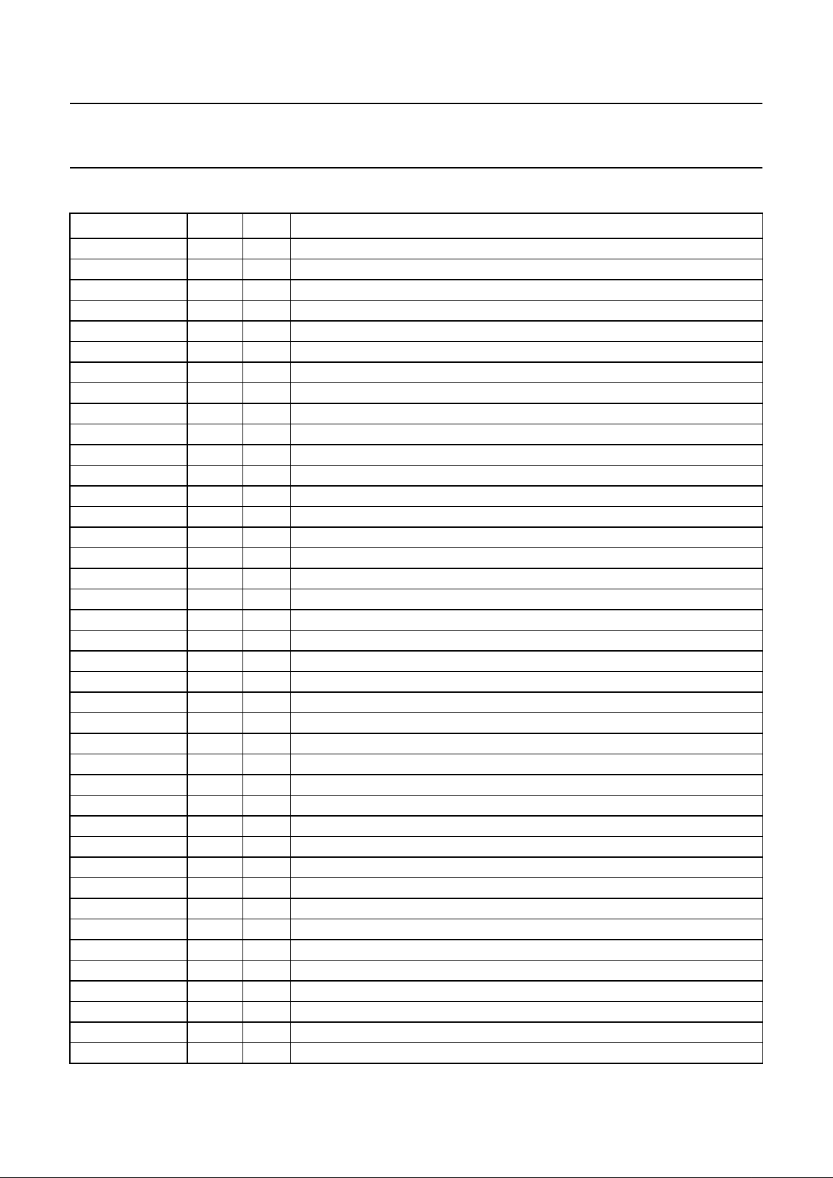
The SAA8110G may be applied together with an analog
front-end (TDA8786 including CDS/AGC/ADC), a timing
generator and a microcontroller as shown in
Figs 18 and 19. Other configurations are also possible.
The CCD-sensor can be of PAL, NTSC or CIF type (with
complementary mosaic colour filter). The maximum
number of active pixels is limited to 800 samples/line.
The 10-bits digital input may have a pixel frequency of up
to 14.318 MHz.
The SAA8110G output data is available in a digital and an
analog output format. Two digital output formats are
selectable: DTV2 (CCIR-601 at the input pixel frequency)
and D1 (CCIR-656 at twice the input pixel frequency). It is
also possible to generate the CIF and QCIF formats as
subsets from the processed CCD-image. The analog
output is available in one of four formats: RGB, YUV, YC
or CVBS. The SAA8110G includes a digital
PAL/NTSC-encoder and 3 DACs for this purpose.
Two types of serial interface are selectable: a fast 400 kHz
I
2
C-bus interfaceor a 80C51 UART interface (with bit rates
from 1 Mbit/s up to 3.75 Mbit/s depending on the system
clock used). The power dissipation of the SAA8110G can
be optimized for each application using the built-in power
management function.
ORDERING INFORMATION
TYPE
NUMBER
PACKAGE
NAME DESCRIPTION VERSION
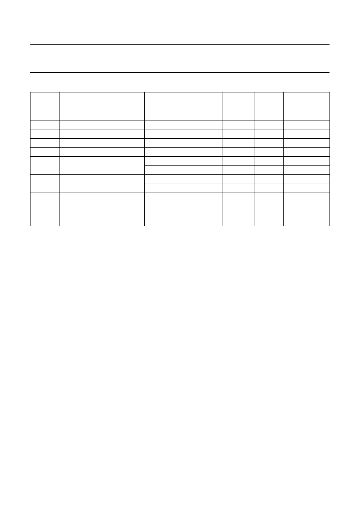
SAA8110G LQFP80 plastic low profile quad flat package; 80 leads; body 12 × 12 × 1.4 mm SOT315-1
1997 Jun 13 3
Philips Semiconductors Preliminary specification
Digital Signal Processor (DSP) for
cameras
SAA8110G
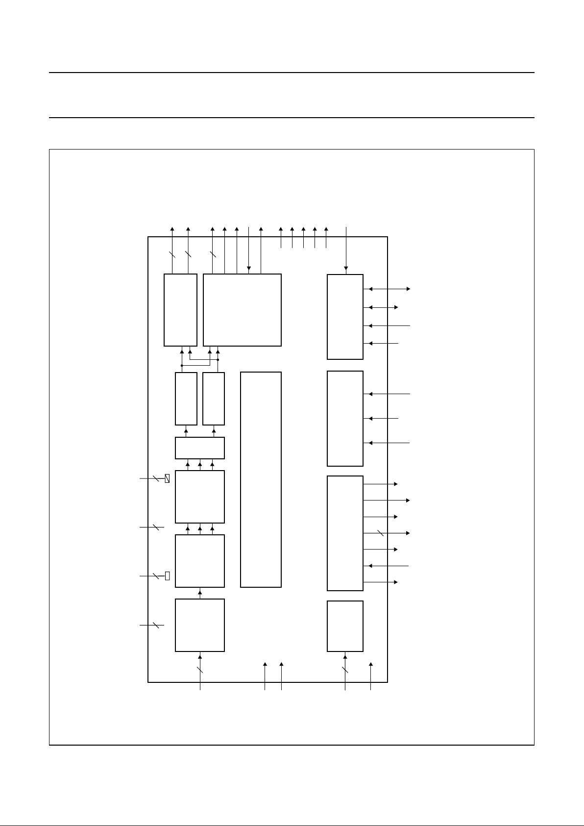
QUICK REFERENCE DATA
Note
1. When digital mode is selected, V
DDA
supply pins can be connected to ground.
SYMBOL PARAMETER CONDITIONS MIN. TYP. MAX. UNIT
V
DDD
digital supply voltage 3 5 5.25 V
V
DDA
analog supply voltage 3 5 5.25 V
V
IL
LOW level digital input voltage 0 − 0.3V
DDD
V
V
IH
HIGH level digital input voltage 0.6V
DDD
− V
DDD
V
V
OL
LOW level digital output voltage IOL = −20 µA −−0.5 V
V
OH
HIGH level digital output voltage IOH = 20 µAV
DDD
− 0.1 −−V
I
DDD(tot)
total digital supply current f
clk
= 14.3 MHz; V
DDD
=5V − 180 200 mA
f
clk
= 14.3 MHz; V
DDD
= 3.3 V − 80 100 mA
I
DDA(tot)
total analog supply current f
clk
= 14.3 MHz; V
DDA
=5V − 30 40 mA
f
clk
= 14.3 MHz; V
DDA
= 3.3 V − 22 35 mA
T
amb
operating ambient temperature 0 − 75 °C
I
DMD
supply current in digital output
mode
f
clk
= 14.3 MHz; V
DDD
=5V;
note 1
− 185 − mA
f
clk
= 14.3 MHz; V
DDD
= 3.3 V − 85 − mA
1997 Jun 13 4
Philips Semiconductors Preliminary specification
Digital Signal Processor (DSP) for
cameras
SAA8110G
BLOCK DIAGRAM
ull pagewidth
MGK158
7 to 16
CCD9toCCD0
CLK1
V
DDD(C1)
V
DDD(C2)
V
DDD(C3)
V
DDD(P1)
V
DDD(P2)
V
SSD(C1)VSSD(C2)VSSD(C3)VSSD(C4)VSSD(P1)VSSD(P2)
V
DDA(BG)
V
DDA(DC)
V
DDA(CD)
V
DDA(O1)
V
DDA(O2)
V
DDA(O3)
V
SSA(CD)
V
SSA(OB)
V
SSA(BG)
1, 29,72,
46, 62
6, 17, 76,
78, 53, 71
45, 41, 22,
40, 38, 36
19, 34,
42
OFFSET
PRE-
PROCESSING
RGB
SEPARATION
(INCL. LINE
MEMORIES)
RGB
PROCESSING
DIGITAL
OUTPUT
FORMATTER
ANALOG
OUTPUT
PREPROCESSING
PAL/NTSC-
ENCODER
V DACs
Y-
PROCESSING
UV-
PROCESSING
RGB
TO
YUV
2
CLK2
47
RESET
31 to 33
T2, T1, T0
MODE
CONTROL
MISCELLANEOUS
FUNCTIONS
SAA8110G
MEASUREMENT ENGINE
30
20 21 25
26,
27
23 24 18
SCLKCDAC
OUT
CDAC
RBIAS
SDATA
STROBE
SMP
P0, P1
VH-REFERENCE WINDOW
TIMING AND CONTROL
345
FI
IN
73 77 75 74
VSYNC
IN
HSYNC
IN
SCL/SN
CL
SDA
A0/SN
DA
A1/SN
RES
SNERT/I
2
C
INTERFACE
SNERT/
I
2
C
SELECT
Y0 to Y7
UV0 to UV7
70 to 63
43
VSYNC
OUT
44
HREF
28
80
4950485251
61 to 54
OUT3 to OUT1
DECOUPL
RBIAS
SIS
79
XINX
OUT
35, 37, 39
LLC
CREF/PXQ
FI
OUT
Fig.1 Block diagram.
1997 Jun 13 5
Philips Semiconductors Preliminary specification
Digital Signal Processor (DSP) for
cameras
SAA8110G
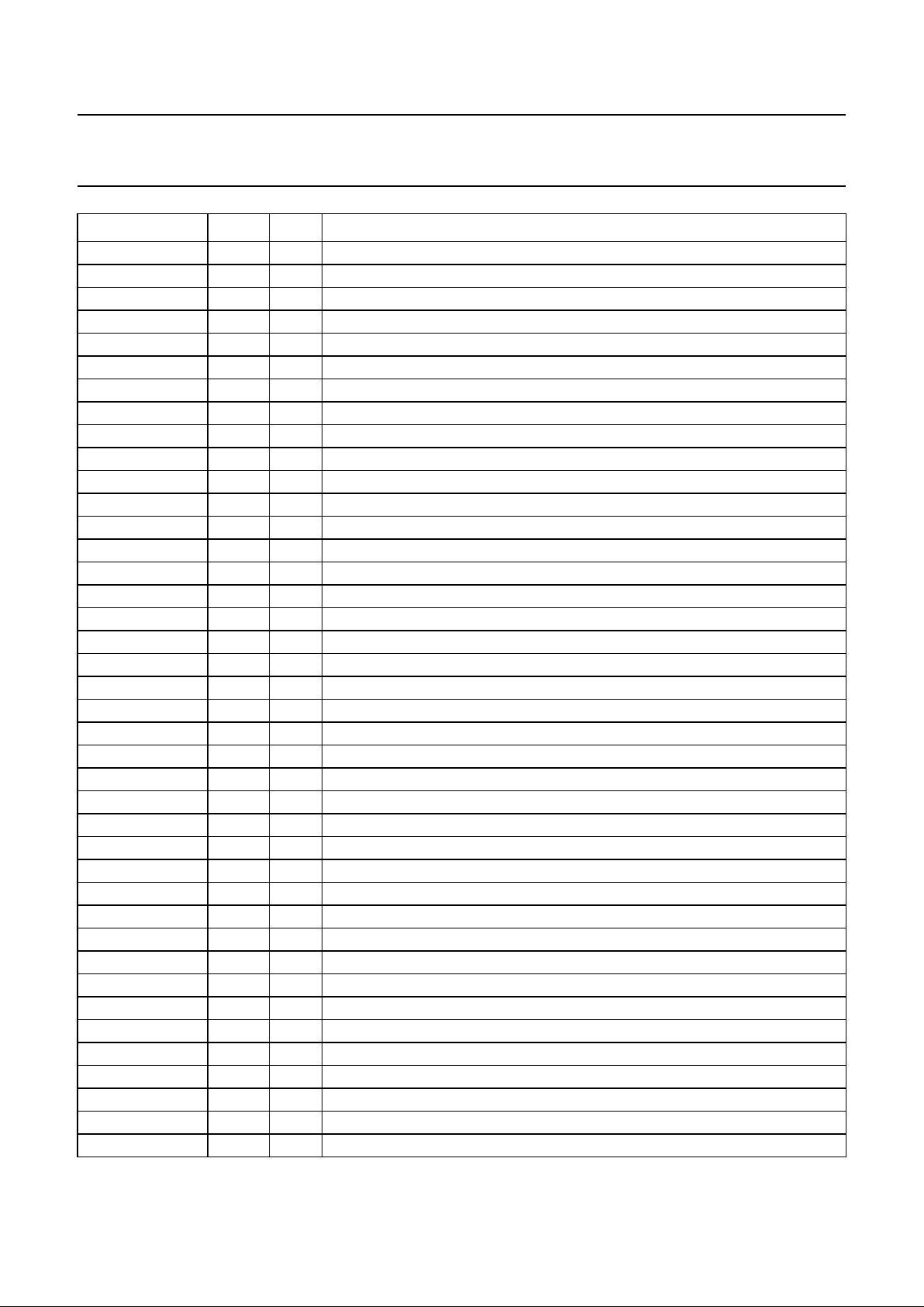
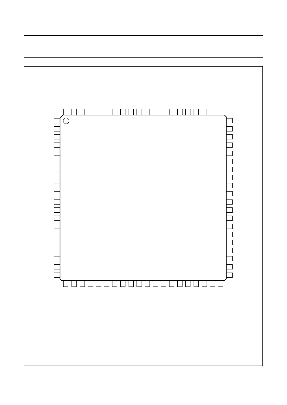
PINNING
SYMBOL PIN I/O DESCRIPTION
V
DDD(C1)
1 I digital supply 1 for digital core and CLK1 related peripherals
CLK1 2 I system- or pixel clock
VSYNC
IN
3 I vertical synchronization input
HSYNC
IN
4 I horizontal synchronization input
FI
IN
5 I field identification signal input
V
SSD(C1)
6 I digital ground 1 for digital core and CLK1 related peripherals
CCD9 7 I (preprocessed) AD-converted CDD-signal bit 9 (MSB)
CCD8 8 I (preprocessed) AD-converted CDD-signal bit 8
CCD7 9 I (preprocessed) AD-converted CDD-signal bit 7
CCD6 10 I (preprocessed) AD-converted CDD-signal bit 6
CCD5 11 I (preprocessed) AD-converted CDD-signal bit 5
CCD4 12 I (preprocessed) AD-converted CDD-signal bit 4
CCD3 13 I (preprocessed) AD-converted CDD-signal bit 3
CCD2 14 I (preprocessed) AD-converted CDD-signal bit 2
CCD1 15 I (preprocessed) AD-converted CDD-signal bit 1
CCD0 16 I (preprocessed) AD-converted CDD-signal bit 0 (LSB)
V
SSD(C2)
17 I digital ground 2 for digital core and CLK1 related peripherals
SCLK 18 O serial clock to TDA8786
V
SSA(CD)
19 I analog ground for control DAC
CDAC
OUT
20 O output control DAC
CDAC
RBIAS
21 I pin to connect external bias resistor for control DAC
V
DDA(CD)
22 I analog supply for control DAC
SDATA 23 O serial data to TDA8786
STROBE 24 O strobe to TDA8786
SMP 25 O switch mode pulse for DC-DC
P0 26 O quasi-static control output pin 0
P1 27 O quasi-static control output pin 1
SIS 28 I SNERT/I
2
C-bus select input signal
V
DDD(C2)
29 I digital supply 2 for digital core and CLK1 related peripherals
RESET 30 I reset input
T2 31 I test mode control signal bit 2
T1 32 I test mode control signal bit 1
T0 33 I test mode control signal bit 0
V
SSA(OB)
34 I analog ground for the three output buffers
OUT3 35 O output buffer 3 (R, V or CVBS)
V
DDA(O3)
36 I analog supply for output buffer OUT3
OUT2 37 O output buffer 2 (B, U or C)
V
DDA(O2)
38 I analog supply for output buffer OUT2
OUT1 39 O output buffer 1 (G or Y)
V
DDA(O1)
40 I analog supply for output buffer OUT1
1997 Jun 13 6
Philips Semiconductors Preliminary specification
Digital Signal Processor (DSP) for
cameras
SAA8110G
V
DDA(DC)
41 I analog supply for analog core of triple DAC
V
SSA(BG)
42 I analog ground for to band gap
DECOUPL 43 O pin to be used for external decoupling of band gap
RBIAS 44 O external bias resistor connection for band gap
V
DDA(BG)
45 I analog supply for band gap
V
DDD(P1)
46 I digital supply 1 for CLK2 related peripherals
CLK2 47 I output clock (CLK2 frequency is 2 × CLK1 frequency)
FI
OUT
48 O field identification output pulse
VSYNC
OUT
49 O vertical synchronization output
HREF 50 O horizontal reference output for YUV-port
CREF/PXQ 51 O clock/pixel qualifier output for YUV-port
LLC 52 O line-locked system clock output
V
SSD(P1)
53 I digital ground 1 for CLK2 related peripherals
UV7 54 O multiplex chrominance UV bit 7 (MSB)
UV6 55 O multiplex chrominance UV bit 6
UV5 56 O multiplex chrominance UV bit 5
UV4 57 O multiplex chrominance UV bit 4
UV3 58 O multiplex chrominance UV bit 3
UV2 59 O multiplex chrominance UV bit 2
UV1 60 O multiplex chrominance UV bit 1
UV0 61 O multiplex chrominance UV bit 0 (LSB)
V
DDD(P2)
62 I digital supply for CLK2 related peripherals
Y7 63 O luminance Y or multiplexed YUV bit 7 (MSB)
Y6 64 O luminance Y or multiplexed YUV bit 6
Y5 65 O luminance Y or multiplexed YUV bit 5
Y4 66 O luminance Y or multiplexed YUV bit 4
Y3 67 O luminance Y or multiplexed YUV bit 3
Y2 68 O luminance Y or multiplexed YUV bit 2
Y1 69 O luminance Y or multiplexed YUV bit 1
Y0 70 O luminance Y or multiplexed YUV bit 0 (LSB)
V
SSD(P2)
71 I digital ground 2 for to CLK2 related peripherals
V
DDD(C3)
72 I digital supply 3 for digital core and CLK1 related peripherals
A1/SN
RES
73 I I2C-bus address select pin A1 or SNERT reset input
A0/SN
DA
74 I I2C-bus address select pin A0 or SNERT data input/output
SDA 75 I I
2
C-bus data input/output
V
SSD(C3)
76 I digital ground 3 for digital core and CLK1 related peripherals
SCL/SN
CL
77 I I2C-bus clock/SNERT clock input
V
SSD(C4)
78 I digital ground 4 for digital core and CLK1 related peripherals
X
IN
79 I input crystal oscillator for subcarrier lock applications
X
OUT
80 O output crystal oscillator for subcarrier lock applications
SYMBOL PIN I/O DESCRIPTION
1997 Jun 13 7
Philips Semiconductors Preliminary specification
Digital Signal Processor (DSP) for
cameras
SAA8110G
Fig.2 Pin configuration.
handbook, full pagewidth
SAA8110G
MGK151
1
2
3
4
5
6
7
8
9
10
11
12
13
14
15
16
17
18
19
20
60
59
58
57
56
55
54
53
52
51
50
49
48
47
46
45
44
43
42
41
UV1
UV2
UV3
UV4
UV5
UV6
UV7
V
SSD(P1)
LLC
CREF/PXQ
HREF
VSYNC
OUT
FI
OUT
CLK2
V
DDD(P1)
V
DDA(BG)
RBIAS
DECOUPL
V
SSA(BG)
V
DDA(DC)
V
DDD(C1)
CLK1
VSYNC
IN
HSYNC
IN
FI
IN
V
SSD(C1)
CCD9
CCD8
CCD7
CCD6
CCD5
CCD4
CCD3
CCD2
CCD1
CCD0
V
SSD(C2)
SCLK
V
SSA(CD)
CDAC
OUT
21
22
23
24
25
26
27
28
29
30
31
32
33
34
35
36
37
38
39
40
80
79
78
77
76
75
74
73
72
71
70
69
68
67
66
65
64
63
62
61
X
OUTXINVSSD(C4)
SCL/SNCLV
SSD(C3)
SDA
A0/SNDAA1/SN
RES
V
DDD(C3)VSSD(P2)
Y0
Y1
Y2
Y3
Y4
Y5
Y6
Y7
V
DDD(P2)
UV0
CDAC
RBIAS
V
DDA(CD)
SDATA
STROBE
SMP
P0
P1
SIS
V
DDD(C2)
RESET
T2
T1
T0
V
SSA(OB)
OUT3
V
DDA(O3)
OUT2
V
DDA(O2)
OUT1
V
DDA(O1)
1997 Jun 13 8
Philips Semiconductors Preliminary specification
Digital Signal Processor (DSP) for
cameras
SAA8110G
FUNCTIONAL DESCRIPTION
Black offset preprocessing
The input data is clamped within the optical black pixel
area of the CCD. The size of the digital clamp window is
16 pixels by 128 lines (i.e. TDA8786). It is possible to
differentiate black levels for odd/even lines, pixels and
fields. This comes in addition to the analog preprocessing
clamp which is active on the clamp pulse generated by the
external timing circuit. The analog clamp is included in the
TDA8786.
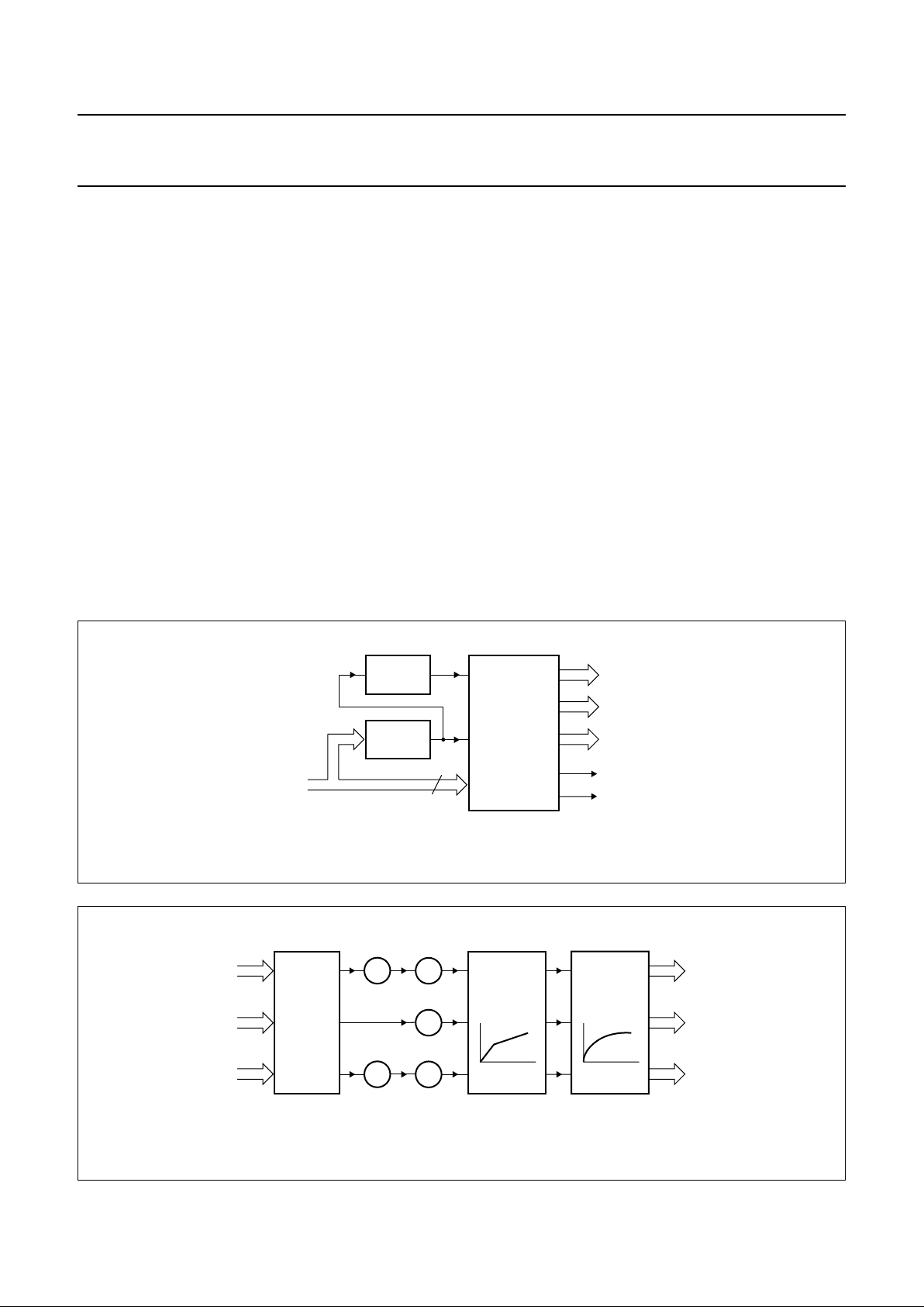
RGB separation
PAL/NTSC sensors generate interlaced data adding offset
in the complementary colour pixels. The RGB separation
block with its two line memories generates the three
components Y, 2R − G, and 2B − G for each input data
corresponding to a pixel value of the CCD. Then the
triplet R, G, B is derived. This block also delivers some
contour and white clip information.
RGB processing
The RGB processing includes several features:
• Colour space matrix depending on CCD type to be
suitable with different sensor colour filters
• Gain correction for R and B signals for white balance
control
• Black offset
• Adjustable knee
• Adjustable gamma function.
The knee function is applied to all three RGB signals.
Its shape is continuously adjustable by changing the slope
and the knee offset point.
To compensate for the non-linear response of display
devices, a gamma correction is applied to R, G and B
signals. It may be adjustable from linear to a 0.35 power
coefficient.
Fig.3 RGB separation diagram.
handbook, full pagewidth
MGK153
LINE
MEMORY
LINE
MEMORY
R
G
B
CCD inputs
white clip
vertical contour
RGB
COLOUR
SEPARATION
10
Fig.4 RGB processing.
handbook, full pagewidth
MGK154
COLOUR
MATRIX
R
R
gainRblack
G
black
G
B
3 ×
KNEE
R
G
B
+
×
+
B
gainBblack
×
+
3 ×
GAMMA
1997 Jun 13 9
Philips Semiconductors Preliminary specification
Digital Signal Processor (DSP) for
cameras
SAA8110G
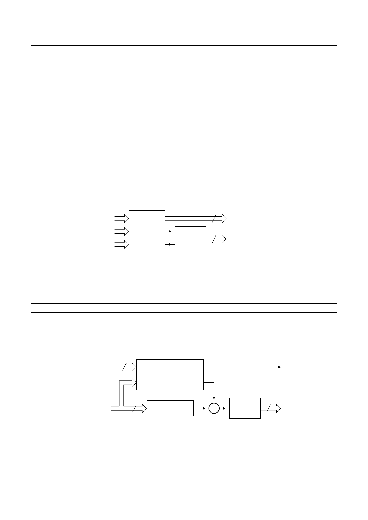
RGB-to-YUV block
After RGB processing, the channels are separated in a
luminance and two colour difference path:
Y = 0.299 R + 0.597 G + 0.114 B, U = 0.49 (B − Y) and
V = 0.88 (R − Y) . It also contains two down-sampling
filters for U and V signals.
Y-processing
The luminance component includes several features:
• Contour correction allowing an increase of the
luminance transitions for a sharper picture
• Black stretch function for contrast enhancement in dark
scenes
• False colour detector used by the UV-processing block
to enable the colour killer
• Filters and noise reduction by coring (only in the high
frequency part of the signal).
Fig.5 RGB-to-YUV conversion.
handbook, full pagewidth
MGK155
Y
(0 to 511)
CONVERSION
MATRIX
DOWN-
SAMPLING
& MUX
9
R
G
B
UV
(−128 to 127)
8
Fig.6 Y processing.
handbook, full pagewidth
MGK156
NOISE
REDUCTION
CONTOUR PROCESSING
AND
FALSE COLOUR DETECTION
BLACK STRETCH
false colour
Y
(0, 0.5 to 255.5)
Y
8
+
9
vertical contour
(−512 to 511)
(from RGB-separation)
10
1997 Jun 13 10
Philips Semiconductors Preliminary specification
Digital Signal Processor (DSP) for
cameras
SAA8110G
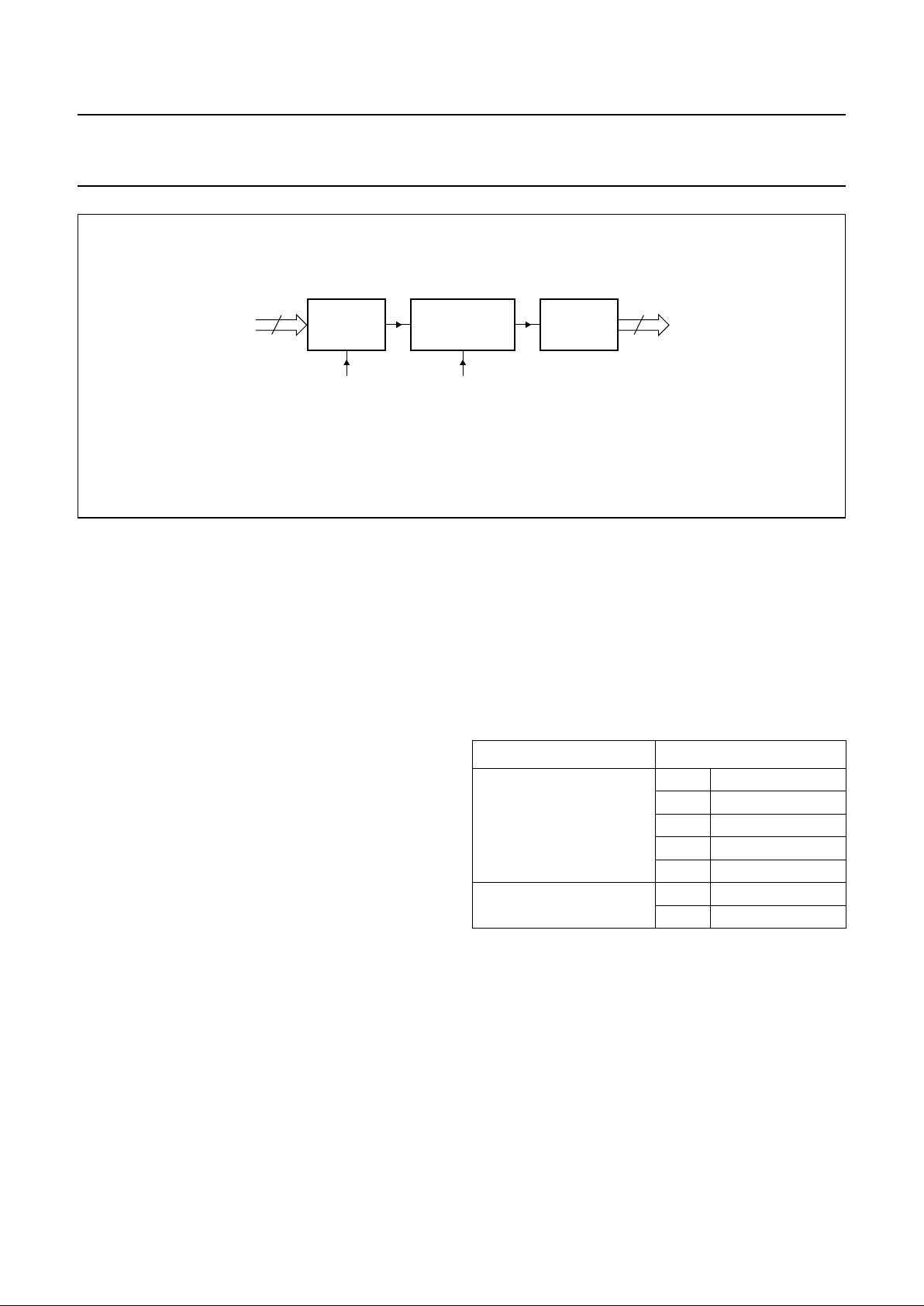
Fig.7 UV-processing.
handbook, full pagewidth
MGK157
UV GAIN
CONTROL
FALSE COLOUR
CORRECTION
NOISE
REDUCTION
false colour
(from Y-processing)
white clip
(from RGB-separation)
UV
(−127 to 128)
8
UV
(−127 to 128)
8
UV-processing
The chrominance component includes several features:
• Noise reduction for high frequencies
• False colour correction: a colour killer cuts the false
colour components in the UV signals
• UV-gain control used to set the correct UV levels for
PAL/NTSC encoding.
As the colour filter saturation levels may be different in the
CCD, the white clip is used in the UV-processing to
suppress colour errors in case of high exposure.
Digital output formatter
This block contains several features:
• Generation of a synchronous clock LLC (twice the clock
frequency)
• Generation of three synchronization signals (HREF,
CREF and VS)
• Synchronization of the output data to the output clock
LLC
• Generation of a CIF/QCIF output format for several type
of sensors (see Table 1)
• Selection of the required digital output format (8-bit
multiplexed YUV standard D1/CCIR 656, including the
generator of SAV/EAV codes or 16-bit multiplexed YUV
4:2:2 standard DTV2/CCIR601).
Note that the D1 frequency data rate is twice the DTV2
frequency data rate.
Moreover, using a high resolution PAL and NTSC CCDs,
it is possible to generate the following formats by means of
cutting or down-sampling.
• CIF 352 × 288 at 25 frame/second and CIF 352 × 240 at
30 frame/second
• QCIF 176 × 144 at 25 frame/second and QCIF
176 × 120 at 30 frame/second.
Table 1 CIF/QCIF output format for different sensor
types
INPUT FORMAT OUTPUT FORMAT
PAL/NTSC-sensor CIF ‘full screen’
CIF ‘zoom-by-2’
QCIF ‘full screen’
QCIF ‘zoom-by-2’
QCIF ‘zoom-by-4’
CIF QCIF ‘full screen’
QCIF ‘zoom-by-2’
1997 Jun 13 11
Philips Semiconductors Preliminary specification
Digital Signal Processor (DSP) for
cameras
SAA8110G
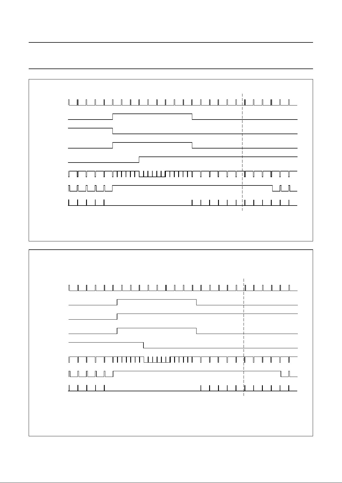
Fig.8 Vertical timing NTSC odd field.
handbook, full pagewidth
MGK159
HSYNC
IN
VSYNC
IN
FI
IN
FI
OUT
VSYNC
OUT
CSYNC
BLANK
BURST
521523525246810121418205225241357911131519212223
Fig.9 Vertical timing NTSC even field.
handbook, full pagewidth
MGK160
HSYNC
IN
VSYNC
IN
FI
IN
FI
OUT
VSYNC
OUT
CSYNC
BLANK
BURST
258 260 262 264 266 268 270 272 274 276 280 282259 261 263 265 267 269 271 273 275 277 281 283 284 285
 Loading...