

Page 1

INTEGRATED CIRCUITS
SAA7785
ThunderBird Avenger PCI Audio
Accelerator
Preliminary specification 1999 Nov 12
Page 2

Philips Semiconductors Preliminary Specification
ThunderBird AvengerTM PCI Audio SAA7785
Accelerator
IEEE 1394 devices via 14 Channel Virtual Write
Master
•Superior hardware acceleration for minimum CPU
consumption
GENERAL DESCRIPTION
The SAA7785 ThunderBird AvengerTM is a high-performance PCI audio accelerator offering the ultimate
home theater, gaming and music solution. Armed with
QSound’s advanced QMSS
transforms ordinary stereo games, movies and music
to 5.1 speaker output. An integrated S/PDIF OUT connects to consumer audio equipment and S/PDIF IN
support provides digital connection from a CD player or
other digital audio equipment. The ThunderBird Aveng-
TM
er
supports redirection of up to 5.1 streams from PCI
to USB or IEEE 1394 devices. Full hardware acceleration of DirectSound
TM
gameport functions provides increased graphic framerates and industry leading low CPU consumption. Utilizing a specialized DSP controller and combining with a
AC97 codec creates a high quality, high performance,
low cost audio subsystem.
TM
, ThunderBird AvengerTM
, 3D audio, music synthesis and
•Broadest API compatibility including
DirectSound3D
TM
, EAXTM, and A3D
TM
•64 hardware wavetable polyphony
•Professional soft-synth with 256 voice polyphony
and XG support
•Second generation ActiMedia programmable DSP
architecture
•Global reverb for external digital and analog input
sources
•Enhanced MIDI reverb and chorus (per track and
global)
2
•Independent I
S input and output ports
•Comprehensive Real Mode DOS and DOS windows support
•Dual gameport accelerator with leagacy and digital
joystick modes
TM
•PC/PCI, DDMA, and LAM
PCI DMA support
•Supports quad and dual AC97 CODECS
FEATURES
•2, 4, or 5.1 speaker and headphone 3D algorithms
TM
•QSound3DInteractive
•QSound Multi-Speaker System
interactive positional 3D
TM
stereo to quad or
•3.3 v operation with 5 v tolerant I/O
(R) 95
•Windows
, Windows
2000 (WDM) drivers
stereo to 5.1 processing
•QSound Environmental Modeling
TM
EAX
1.0/2.0 compatible)
TM
•QXpander
and stereo-to-3D remapping
•Integrated S/PDIF OUT and optional S/PDIF IN
•AC3 5.1 or stereo playback through S/PDI F output
•Processing up to 512 simultaneous inputs including
TM
(I3D Level 2.0,
APPLICATIONS
•Complete audio subsystem when combined with
AC97 CODEC
•PC sound cards and motherboards
•Video games and other PCI bus-based multimedia
applications
256 DirectSound streams and up to 96 concurrent
CD quality 3D streams
•Redirection up to 5.1 streams from PCI to USB or
1999 Nov 12 2
(R)
98, and Windows
(R)
Page 3

Philips Semiconductors Preliminary Specification
ThunderBird AvengerTM PCI Audio SAA7785
Accelerator
ORDERING INFORMATION
TYPE
NUMBER
NAME DESCRIPTION VERSION
PACKAGE
SAA7785 TQFP128 Thin quad flat pack; 128 leads (lead length 1.00 mm); body
14 x 14 x 1.00 mm
SAA7785 TQFP100 Thin quad flat pack; 100 leads (lead length 1.00 mm); body
14 x 14 x 1.00 mm
QUICK REFERENCE DATA
Condition Symbol Maximum Ratings
Ambient Operating Temperature T
Ambient Storage Temperature T
A
S
Non-Operating Core and Ring Supply Voltage VDD, VDDIC -0.5V to 4.6V *
Operating Core Supply Voltage VDDIC -0.5V to 3.63V *
0°C to +70°C
-65°C to +150°C
25-90040
25-90042
Operating Ring Supply Voltage VDD 3.0V to 3.63V *
5V Tolerant Supply (5.0V nominal supply) NWELL -0.5V to 5.5V *
NWELL to VDD Differential NWELL-VDD 0 ≤ (NWE LL-V DD) < 4.0V
3V Tolerant I/O DC Input Voltage V
3V Tolerant I/O DC Output Voltage V
5V Tolerant I/O DC Input Voltage V
5V Tolerant I/O DC Output Voltage V
DC Input Current (at V
DC Output Current (at V
< 0V or VI > VDD) I
I
< 0V or VO > VDD) I
O
Power Dissipation P
I3
O3
I5
O5
I
O
D
-0.5V to VDD+0.5V (≤ 4.6V max)+
-0.5V to VDD+0.5V (≤ 4.6V max)+
-0.5V to 5.5V (≤ 6.0V max)+
-0.5V to VDD+0.5V (≤ 4.6V max)+
± 20mA
± 20mA
500mW
*Refer to Section 3.1 to ensure proper power supply sequencing as well as voltage ranges.
+Items in parenthesis are non-operating conditions.
1999 Nov 12 3
Page 4
Philips Semiconductors Preliminary Specification
ThunderBird AvengerTM PCI Audio SAA7785
Accelerator
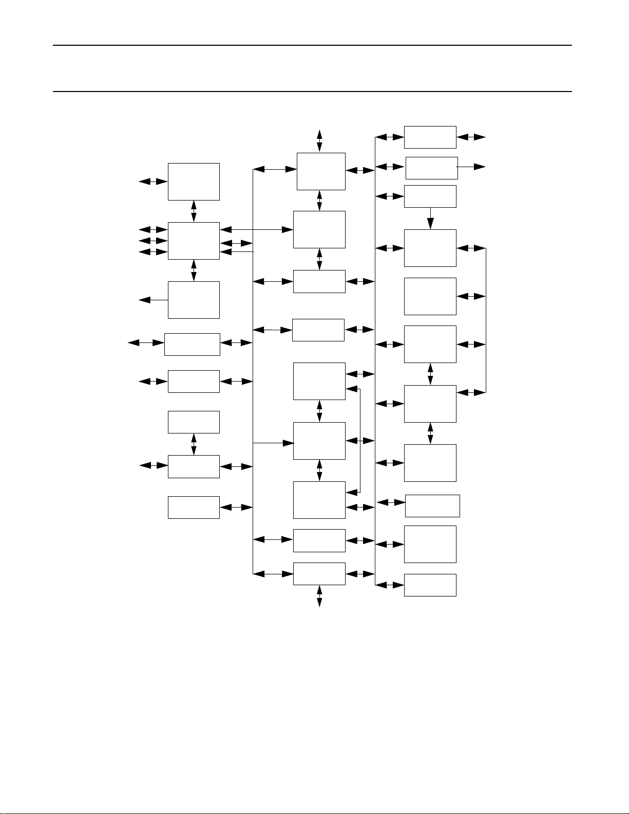
FIGURE 1 BLOCK DIAGRAM
Serial
CFG
Port
PCI
Bus
Test
Port
INTA#
GPIO
GamePort
AC97
Xtal_out
PCI
Configuration
Headers
PCI
Master/Slave
Interface
Serial
Interrupt
Controller
General
Purpose I/O
Game Port
Interface
PLL
Test Logic
PLL Cell
AC Link Interface
AC LINK
Legacy
DMA
Interface
SoundBlaster
Registers
OPL3
Registers
Sample Fetch
Accelerator
Virtual
Registers
I2S
Interface
S/P DIF
Output
DSP Interrupt
Controller
INTRs
DSP DATA BUS
DSP Core
DSP Code
ROM
DSP Code
RAM
DSP
Memory
Controller
DSP Data
RAM
2
S
I
Port
S/P DIF
DSP CODE BUS
Multimedia
Timer
Address
Generation
Host/DSP
Interface
MIDI Regs
and UART
MIDI Interface
1999 Nov 12 4
FM
Accelerator
Prog
IIR Filter
Phase/Env
Accelerator
Page 5

Philips Semiconductors Preliminary Specification
ThunderBird AvengerTM PCI Audio SAA7785
Accelerator
PINNING
TABLE 1 Signal and Pin Names for 128 pin SAA7785 ThunderBird Avenger
PIN
#
1 BIT_CLK 33 GNT# 65 AD22 97 AD12
2 SDATA_OUT
3 SDATA_IN0 35 RST# 67 AD21 99 AD10
4 SDATA_IN1 36 VSS 68 AD20 100 NWELL1
5 AC_RST# 37 PCLK 69 AD19 101 PGPIO4
6 VSS 38 PCGNT# 70 VSS 102 AD9
7 JAB1 39 PCREQ# 71 AD18 103 VDD
8 JBB1 40 VDD 72 AD17 104 AD8
9 VDD 41 GNT# 73 AD16 105 VSS
10 JACX 42 VDDIC 74 PGPIO7 106 C/BE0
11 JBCX 43 REQ# 75 NWELL3 107 VDDIC
12 MIDIOUT 44 PGPIO0 76 VSS 108 AD7
13 JBCY 45 AD13 77 C/BE2# 109 VDD
14 NWELL2 46 AD30 78 FRAME# 110 AD6
15 JACY 47 VDD 79 VDD 111 AD5
16 VSSIC 48 PGPIO1 80 IRDY# 112 VSS
17 JBB2 49 AD29 81 PGPIO6 113 AD4
18 TRI#/CFGCLK 50 VSS 82 VDDIC 114 AD3
19 MIDIIN 51 NWELL0 83 TRDY# 115 AD2
20 VDD 52 PGPIO2 84 VSS 116 VSSIC
21 VSS 53 AD28 85 DEVSEL# 117 AD1
22 TRI#/CFGCLK 54 VSSIC 86 STOP# 118 AD0
23 NAND#/CFGDAT 55 AD27 87 PGPIO5 119 VDD
24 SPDO 56 VDD 88 VDD 120 TWS
25 CCLK 57 AD26 89 PERR# 121 TSD
26 DSPCLK 58 VSS 90 SERR# 122 TSCK
27 SPDI 59 AD25 91 PAR 123 CLKRUN
28 VDD 60 AD24 92 C/BE1 124 RESVDS
29 VSS 61 C/BE3# 93 AD15 125 RSD/GPIO2
30 PSUB 62 IDSEL
31 PLLAPWR 63 AD23 95 VSS 127 RWS/GPIO0
32 PLLAGND 64 PGPIO3 96 AD13 128 SYNC
PIN NAME
34 PME# 66 VDD 98 AD11
94 AD14 126 RSCK/GPIO1
TM
1999 Nov 12 5
Page 6

Philips Semiconductors Preliminary Specification
ThunderBird AvengerTM PCI Audio SAA7785
Accelerator
FIGURE 2 PIN CONFIGURATION
SAA7785 ThunderBird AvengerTM PINS ON 128 PIN TQFP PACKAGE DIAGRAM (TOP VIEW).
RESVD
CLKRUN#
TSCK
TSD
TWS
VDD
AD0
AD1
VSSIC
AD2
AD3
AD4
VSS
AD5
AD6
VDD
AD7
VDDIC
C/BE0#
VSS
AD8
VDD
AD9
PGPIO4
NWELL
AD10
SDATA_OUT
SDATA_IN0
SDATA_IN1
TRI#/CFGCLK
NAND#/CFGDAT
Notes:
1. Package body size is 14 mm.
2. Scale is approx 1” = 5.08 mm (5X actual size).
3. Use package bond form nuber 23-xxxxx.
BIT_CLK
AC_RST#
VSS
JAB1
JBB1
VDD
JACX
JBCX
MIDIOUT
JBCY
NWELL
JACY
VSSIC
JBB2
JAB2
MIDIIN
VDD
VSS
SPDO
CCLK
DSPCLK
SPDI
VDD
VSS
PSUB
PLLAPWR
PLLAGND
RSD/DGPIO2
RSCK/DGPIO1
SYNC
RWS/DGPIO0
12897127
126
125
124
123
122
121
120
119
118
117
116
115
114
113
112
111
110
109
108
107
106
105
1
2
3
4
5
6
7
8
9
10
11
12
13
14
15
16
17
18
19
20
21
22
23
24
25
26
27
28
29
30
31
32
33643435363738394041424344454647484950515253545556575859606162
VSS
RST#
INTA#
PME#
SAA7785
128 PIN TQFP
VSS
REQ#
VDDIC
VDD
AD31
AD30
AD29
PGPIO0
NWELL
PGPIO1
VDD
PCLK
GNT#
PCGNT#
PCREQ#
104
VDD
AD28
AD27
AD26
VSSIC
PGPIO2
103
VSS
102
AD25
101
AD24
100
C/BE3#
AD11
AD12
99
98
AD13
96
VSS
95
AD14
94
AD15
93
C/BE1#
92
PAR
91
SERR#
90
PERR#
89
VDD
88
PGPIO5
87
STOP#
86
DEVSEL#
85
VSS
84
TRDY#
83
VDDIC
82
PGPIO6
81
IRDY#
80
VDD
79
FRAME#
78
C/BE2#
77
VSS
76
NWELL
75
PGPIO7
74
AD16
73
AD17
72
AD18
71
VSS
70
AD19
69
AD20
68
AD21
67
VDD
66
AD22
65
63
AD23
IDSEL
PGPIO3
1999 Nov 12 6
Page 7

Philips Semiconductors Preliminary Specification
ThunderBird AvengerTM PCI Audio SAA7785
Accelerator
PINNING
TABLE 2 PIN DEFINITIONS FOR THE 100 Pin SAA7785 ThunderBird Avenger
PIN
#
1 BIT_CLK 30 PCLK 59 VSS 87 AD5
2 SDATA_OUT 31 PCGNT# 60 C/BE2# 88 VSS
3 SDATA_IN 32 PCREQ# 61 FRAME# 89 AD4
4 AC_RST# 33 GNT# 62 IRDY# 90 AD3
5 VSS
6 JAB1 35 REQ# 64 TRDY# 92 VSSIC
7 JBB1 36 AD31 65 DEVSEL# 93 AD1
8JACX 37AD30
9JBCX 38VDD 67VDD 95VDD
10 MIDIOUT 39 AD29 68 PERR# 96 CLKRUN#
11 JBCY 40 NWELL_40 69 SERR# 97 RSD/GPIO2
12 JACY 41 AD28 70 PAR 98 RSCK/GPIO1
13 VSSIC 42 VSSIC 71 C/BE1# 99 RWS/GPIO0
14 JBB2 43 AD27 72 AD15 100 SYNC
15 JAB2 44 AD26 73 AD14
16 MIDIIN 45 VSS 74 VSS
17VDD 46AD25 75AD13
18 TRI#/CFGCLK 47 AD24 76 AD12
19 NAND#/CFGDAT 48 C/BE3# 77 AD11
20 SPDO 49 IDSEL 78 AD10
21 CCLK 50 AD23 79 NWELL1
22 DSPCLK 51 AD22 80 AD9
23 PSUB 52 VDD 81 VDD
24 PLLAPWR 53 AD21 82 AD8
25 PLLAGND 54 AD20 83 C/BE0#
26 INTA# 55 AD19 84 VDDIC
27 PME# 56 AD18 85 AD7
28 RST# 57 AD17 86 AD6
29 VSS 58 AD16
PIN NAME
34 VDDIC 63 VDDIC 91 AD2
66 STOP# 94 AD0
TM
1999 Nov 12 7
Page 8

Philips Semiconductors Preliminary Specification
ThunderBird AvengerTM PCI Audio SAA7785
Accelerator
SAA7785 ThunderBird AvengerTM pinout for 100 pin package
RSCK/DGPIO1
RSD/DGPIO2
CLKRUN#
VDD
AD0
AD1
VSSIC
AD2
AD3
AD4
VSS
AD5
AD6
AD7
VDDIC
C/BE0#
AD8
VDD
AD9
NWELL
AD10
AD11
SYNC
RWS/DGPIO0
AD12
BIT_CLK
SDATA_OUT
SDATA_IN0
AC_RST#
MIDIOUT
TRI#/CFGCLK
NAND#/CFGDAT
DSPCLK
PLLAPWR
PLLAGND
Notes:
1. Package body size is 14 mm.
2. Scale is approx 1” = 5.08 mm (5X actual size).
3. Use package bond form nuber 23-61269.
VSS
JAB1
JBB1
JACX
JBCX
JBCY
JACY
VSSIC
JBB2
JAB2
MIDIIN
VDD
SPDO
CCLK
PSUB
9998979695949392919089888786858483828180797877
100
1
2
3
4
5
6
7
8
9
10
11
12
13
14
15
16
17
18
19
20
21
22
23
24
25
26272829303132333435363738394041424344454647484950
RST#
INTA#
PME#
SAA7785
100 PIN TQFP
VSS
PCLK
GNT#
PCGNT#
PCREQ#
REQ#
VDDIC
VDD
AD31
AD30
AD29
NWELL
VSS
AD28
AD27
AD26
AD25
VSSIC
76
AD13
75
VSS
74
AD14
73
AD15
72
C/BE1#
71
PAR
70
SERR#
69
PERR#
68
VDD
67
STOP#
66
DEVSEL#
65
64
TRDY#
63
VDDIC
62
IRDY#
61
FRAME#
60
C/BE2#
59
VSS
58
AD16
57
AD17
56
AD18
55
AD19
54
AD20
53
AD21
52
VDD
51
AD22
AD24
AD23
IDSEL
C/BE3#
1999 Nov 12 8
Page 9

Philips Semiconductors Preliminary Specification
ThunderBird AvengerTM PCI Audio SAA7785
Accelerator
FUNCTIONAL OVERVIEW
QSound 3D Audio Algorithms
QSound Labs most advanced algorithms for 3D
virtualization, multichannel processing, audio mixing
and wavetable synthesis result in unsurpassed 3D
audio. QSound’s Q3D
natively for speakers and therefore requires no
crosstalk cancellation. The result is a wide “sweetspot”,
strong positional perception and insensitivity to head
movement and position. Listeners can enjoy a true 3D
experience with only two speakers connected to their
PC.
QSound Multi-Speaker System
proprietary stereo-to-quad or 5.1 remapping algorithm
to transform ordinary stereo into more immersive quad
and 5.1 outputs. Not simply mirroring the front speaker
output to the rear speakers, QMSS
individual channels. The result is DirectSound games
become more realistic with action all around the
listener; music CD, MP3 and MIDI playback become
more immersive; and stereo and Dolby ProLogic film
clips become theatre-like in presentation without
needing a specific decoder.
QSound3DInteractive
to interactively position DirectSound streams in 3D
space around the listener. Four different 3D engines,
based on HRTF and patented QSound technology,
render sound over headphones, 2, 4 or 5.1 speakers.
TM
Q3DI
uses the industry standard DirectSound3DTM
API and is compatible with DirectSound, EAX
A3D1.0
TM
applications.
QSound Environmental Modeling
further realism by adding reverb, occulsion and
obstruction as additional positional ques. With QEM
enabled, each DirectSound3D sound source receives
reverb simulating acoustic reflections based on the
regions reverb present and the sources’ current
position relative to the listener. In addition obstruction
and occlusion filters are used to simulate the acoustical
effects of barriers and openings in a games virtual 3D
environment such as walls, doorways and pillars, and
is compliant with I3D Level 2.0.
S/PDIF OUT/IN
The SAA7785 ThunderBird Avenger
integrated S/PDIF OUT port enabling users to output
TM
is the only solution developed
TM
(QMSSTM) uses a
TM
creates 4 and 5.1
TM
utilizes the ActiMediaTM DSP
TM
, and
TM
(QEMTM) adds
TM
provides an
AC3 data from a DVD directly to an AC3 decoder.
The S/PDIF stereo output capability allows users to
connect to a variety of consumer audio equipment ,
such as a stereo receiv er, minidisk, or digital
speakers. S/PDIF IN support through the I
2
S port
enables digital connection from a CD player or other
audio equipment that utilizes the S/PDIF format.
Superior Concurrency
The SAA7785 ThunderBird Avenger
TM
combines its
64 hardware input buffers with software (256 MIDI
channels and 192 DirectSound
TM
inputs) for a total of
512 simultaneous streams. The ThunderBird
Avenger
TM
can process 64 combined audio and
wavetable voices in hardware plus an additional 192
audio streams using QSound’s efficient MMX host
engine. In addition, Avenger offers game developers
up to 96 simultaneous 3D streams. For greater
concurrency and higher music polyphony a
professional quality 256 voice soft-synth is available.
This can be used for all music synthesis reserving all
256 streams for other audio sources, making the
ThunderBird Avenger
TM
an excellent solution for
gaming applications.
Hardware Acceleration
The SSA7785 ThunderBird Avenger
TM
is a true
hardware audio accelerator. CPU consumption is
minimized by processing sample rate conversion,
panning, mixing, 3D virtualization, filtering, music
synthesis, multichannel conversion, and gameport
functions in the hardware DSP. This frees up the host
CPU to perform other tasks, boosting graphic frame
rates and raising system benchmarks.
320 Voice CD Quality Wavetable Synthesis
ThunderBird Avenger
TM
includes two wavetable
synthesis engines. When hardware mode is enabled,
the ActiMedia
TM
DSP can produce up to 64
wavetable 44Khz, 16 bit voices. This mode
minimizes CPU consumption and is ideal for games
with MIDI music tracks. In addition, a professional
quality soft-synth can produce up t o 256 voices
including special effects. The soft-synth is
configurable and can be optimized for highest quality
with pure music applications or for minimum CPU
consumption in gaming applications. Combining both
hardware and software synthesizers allows for 320
1999 Nov 12 9
Page 10

Philips Semiconductors Preliminary Specification
ThunderBird AvengerTM PCI Audio SAA7785
Accelerator
total simultaneous voices.
ActiMedia
ActiMedia
TM
DSP Architecture
TM
DSP architecture combines the strengt hs
of programmable and fixed function DSP architectures.
Programmability enables custom features, field
upgrades, and simple application development, while
an array of gate-efficient fixed function DSP processors
(accelerators) operate in parallel to provide an
excellent price/performance ratio. Unlike fixed-point
DSPs that must use a single resolution for all audio
processing, each accelerator is designed with the
optimum resolution for its function. This provides audio
integrity without the cost of high resolution or floating
point programmable DSP implementation.
Digital Model Dual Game Port
The software polling used by analog game ports can
consume up to 10% of the host CPU. ThunderBird PCI
products utilize a digital operation mode that can
eliminate software polling and accelerate the game
port function resulting in significan tly impr ove d syste m
performance. Joystick buttons can be polled or
interrupt driven to further enhance performance. A
default analog mode assures compatibility with DOS
and other non-DirectInput
TM
applications.
Comprehensive Legacy Audio Support
SoundBlaster Pro compatibility in both Real Mode DOS
and DOS windows is achieved through hardware
SoundBlaster and OPL3 (FM) emulation registers.
Legacy DMA over the PCI bus is supported on all
major platforms utilizing PC/PCI, DDMA, or Philips’
proprietary Legacy Accommodation Mode
TM
(LAMTM).
DOS music synthesis includes stereo MIDI playback
and quad/5.1 MIDI playback as well as FM emulation.
1999 Nov 12 10
Page 11
Philips Semiconductors Preliminary Specification
ThunderBird AvengerTM PCI Audio SAA7785
Accelerator
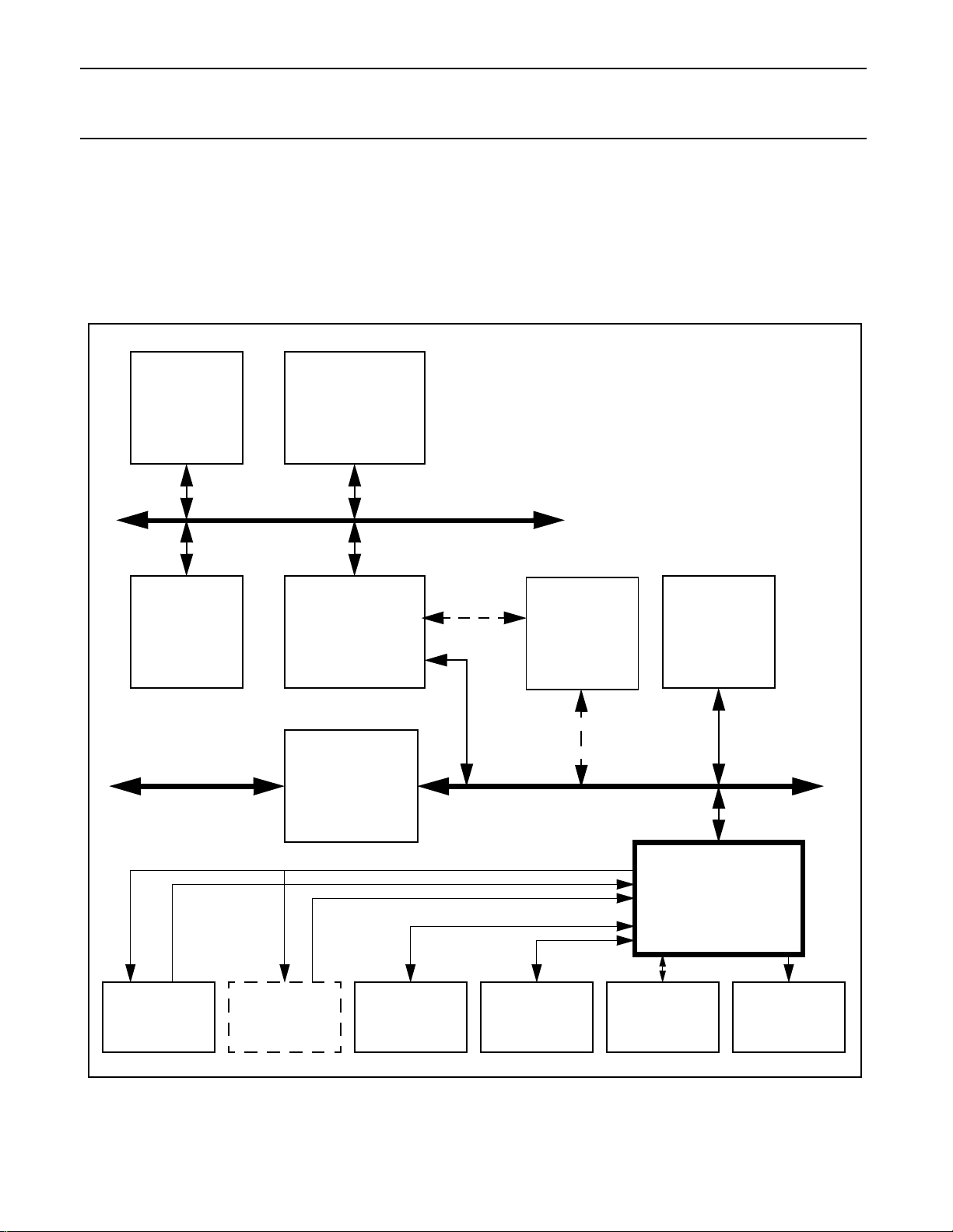
Architectural Overview
The SAA7785 ThunderBird AvengerTM is a multi-functional device that provides sound processing producing SoundBlaster-compatible emulation, DirectSound acceleration, 3D sound, spatialization, special effects, and 64-voice wavet able synthesis through the use of a Pine Digital Signal Processor (DSP) as the primary engine. Included within the
ThunderBird Q3DIII are interfaces for an AC97 codec, I
Consumer Output port.
FIGURE 3 Block Diagram of a PC/AT System with the SAA7785 ThunderBird AvengerTM
2
S I/O, MIDI port, standard analog joyst icks, and an S/P DI F
CPU
System
Bridge
TM
HOST BUS
AGP
Graphics
Cache
Memory
ISA BUS PCI BUS
Pentium
Controller
PCI to ISA
Multi I/O
AC97 CODEC
2/4 Channels Additional
(Primary)
1999 Nov 12 11
AC97 CODEC
2 channels
ThunderBirdTM Audio
Controller
JoystickMIDI Port
I2S S/P DIF
Page 12

Philips Semiconductors Preliminary Specification
ThunderBird AvengerTM PCI Audio SAA7785
Accelerator
TM
The SAA7785 ThunderBird Avenger
port. Software support is required for non-DOS applications, such as Windows
tem can also be supported with the additional software.
chip is designed to operate on any PCI system with the proper software sup-
(tm)
drivers. Non Pentium
(tm)
based sys-
Systems that provide DDMA or have the ISA bridge on the primary PCI bus are able to perform SoundBlaster emulation
enabling the operation of legacy DOS based games. The SAA7785 ThunderBird Avenger
TM
chip provides two 8237
style DMA channels to perform legacy DMA cycles on selected syst ems. The s ame t wo 8237 c hannels provide Dist ributed DMA support as well. PC/PCI is also supported to provide legacy DMA support on chipsets that support said protocol. For systems that support neither DDMA nor PC/P CI, there is a sof tw are solution implemented as a TSR.
DirectSound acceleration, both for 2D and 3D audio along with wavetable sample fetching, is accomplished using the
SAA7785 ThunderBird Avenger
ThunderBird Avenger
TM
chip to accelerate DirectSound audio streams as well as fet ch wav etable sample for the 64
TM
chip PCI 2.1 bus master. This bus master provides the means for the SAA7785
voice wavetable synthesis and effects algorithms. Wavetable sample fetching is always retrieved from system memory
saving the cost of an external wavetable ROM. Downloadable sample sets, with software, are also supported using the
bus master hardware.
Additionally, the SAA7785 ThunderBird Avenger
TM
chip follows the AC97 Architecture to provide high quality audio by
the use of one or more separate codecs. Serial DACs, as well as AC97 CODECs can be selected to providing audio
into the analog world for low cost playback. Multi-channel AC97 CODECs can be us ed to provide up to 8 c hannels of
audio output.
A programmable DSP core is also provided to run the audio algorithms for wavetable synthes is, FM s ynthesis, s pecial
effects such as reverb and chorus, along with sample rate conversion and data management. The imbedded DSP core
and its peripherals are managed solely by the DSP and requires no intervention from the host. The host can DS P can
pass messages to and from each domain to provide a host s oftware interf ace into t he DSP domain.
PCI Interface, Configuration, and Interrupt Serializer
The SAA7785 ThunderBird AvengerTM chip PCI interface is composed of master and slave state machines, an
address/data/byte enable datapath, a bus arbiter for the two on chip masters, control logic for the master and slave
internal busses, an interrupt serializer, and the standard PC I configurat ion register header.
The standard PCI configuration header is also supported. Since the SAA7785 ThunderBird Avenger
tion device, there are three PCI configuration spaces allocated f or each funct ion. The three func tions are t he audio
device, the joystick and the 16650 UART. The purpose of the mult iple configuration headers is to ensure PCI c ompliance and enable the operating system to select the correct sof tw are driver for each individual device. The Serial CFG
Port is used to shift in subvendor specific data for each of the PCI configuration headers. The Serial CFG port is an
industry standard I
2CTM
format. The configuration headers are included in the PCI interface to reduc e inter-block rout-
ing. All other PCI configuration space registers are included in the blocks that utilize these registers.
TM
is a multi-func-
Clocks and the PLL Subsystem
Clocks for operation of the SAA7785 ThunderBird AvengerTM are derived from two sources; an external crystal and bit
clock from the AC97 CODEC. The SA A7785 ThunderBird Avenger
external crystal.
TM
The SAA7785 ThunderBird Avenger
substem consists of a fixed layout PLL cell and a digital interface to the 8 bit PS
bus. The PLL is designed to drive the clocks for the DSP subsystem. The implementation calls for the PLL to be utilized
with complete programmable register interface to enable the tuning of the frequencies as necessary.
TM
PLL Subsystem derives its reference from the
Multimedia Timer
The SAA7785 ThunderBird AvengerTM chip supplies a 20-bit, .84 uS resolution timer for game synchronization. The
1999 Nov 12 12
Page 13

Philips Semiconductors Preliminary Specification
ThunderBird AvengerTM PCI Audio SAA7785
Accelerator
timer data can be accessed as an I/O device. This timer can be used by game developers to keep track of time elapsed
to synchronize the video to the audio stream. The timer can be polled or interrupt driven and is selectable by the user
application.
DMA
DMA is for the Sound Blast er registers, t he DSP Mastering Dev ice (DMD), and the S/P DI F output. To cover as many
systems as possible, the DMA interface supports three modes for legacy s upport: Mobile PC /PCI DMA Arbitrat ion
(PC/PCI), Distributed DMA (DDMA) and Legacy Accommodation Mode (LAM).
Legacy Accommodation Mode allows the SAA7785 ThunderBird Avenger
snoop and snarf selected DMA cycles on the PCI bus that were intended to the ISA B ridge. I f a chip set support s Distributed DMA, the SAA7785 ThunderBird Avenger
ally, PC/PCI can be utilized as well if neither DDMA nor LAM are supported on the selected chip set.
TM
will use this method since it is more efficient than LAM. Addition-
TM
, in an architecturally compatible system, to
AC Link
The SAA7785 ThunderBird AvengerTM chip provides support for the AC97 (V2.1) specification by supplying an AC Link
interface to communicate with industry standard AC97 CODECs. Up to two CODECs can be used for a total of 8 possible outputs (4 stereo channels).
Sound Blaster Registers
The other device that requires DMA is the SoundBlaster registers. DMA is used to transfer SoundBlaster digital audio
files from the host to a codec for playback in addition to prov iding a mailbox for other commands. In order for the DSP
to emulate the Sound Blaster sound effects, a legacy register set must be implemented to capture these commands.
These sixteen, 16-bit registers are used primarily to emulate SoundBlaster Pro register set as well as the SoundBlaster
Pro mixer registers. These registers are used as a mailbox to the DSP dat a bus to deliver data to the SoundB laster
Emulation code. The SAA7785 ThunderBird Avenger
requires. All data transmitted over the SoundBlaster Registers is processed by the DSP to emulate the Sound Blaster
Pro hardware.
TM
chip supports DMA to the Sound Blaster that legacy code
OPL3 Registers and the FM Accelerators
The OPL3 register interface is a subset of the complete SoundBlaster register set . The OPL3 regist ers are separat e to
point out that the FM legacy is supported at the register level. The OPL3 registers simply pass FM synthesis commands
to the SoundBlaster Emulation code and receive status from t he same code.
Virtual Registers
The Virtual Registers interfaces the PCI bus and two substantial wavetable synthesis accelerators: the Sample Fetc h
and Address Generation accelerators. The Virtual Registers is responsible for setting up the PCI interfac e for master
cycles data fetches and retrieving those fetches int o a s ample buffer. The Virt ual Registers get commands from the
Address Generation accelerator and turns them into PCI master requests. Once the data has been retrieved, the Virtual
Register then instructs the Sample Fetch ac celerator to process a block of dat a. Once t he processing is complete, the
Sample Fetch Accelerator notifies the Virtual Registers that all is clear and that new data can be processed.
Address Generation Accelerator
The Address Generation accelerator is a preprocessing unit for the sample f etching mechanism inside the Virtual Registers. The Address Generator will get a set of parameters from the DS P code on a per voice basis for either DirectSound processing or wavetable synthesis. Once these voice parameters are set, the hardware is instructed to translate
1999 Nov 12 13
Page 14

Philips Semiconductors Preliminary Specification
ThunderBird AvengerTM PCI Audio SAA7785
Accelerator
the addresses and fetch the audio samples from system memory. The Address Generator is also capable of looping
without intervention from the DSP code. The DSP kills voices by instruct ing t he Address Generator to s top fet c hing
data. Once the samples are fetched, they are stored in the Virtual Register’s input sample buffer for processing by t he
Sample Fetch Accelerator.
Sample Fetch Accelerator
The Sample Fetch accelerator is used to process audio samples fetched by the Virtual Registers and deliver them t o
the DSP code for further processing. This processing can include pitch shifting or sample rate conversion. The degree
of pitch shifting is under direction of DSP code indicating the Sample Fetch accelerator is programmable. The input
samples are taken from the Virtual Register’s input sample buffer and stored in DSP memory space.
MIDI Registers and UART
An MPU401 compatible UART is supplied to enable external MIDI devices to use the SAA7785 ThunderBird AvengerTM
chip synthesizers as well as its external device’s own synthesizer. The MIDI register interface is used to pass the MIDI
command stream from the host to the DSP firmware for parsing into synthesizer commands. The MPU401 UA RT
always operates in “dumb” mode. Both the PCI and DSP can access the MIDI UART directly. Data is presented from/to
the MPU401 Registers in a mailbox fashion to the MPU401 UART.
General Purpose Input/Output
There are seven general purpose I/O pins that are controlled by the PCI bus (128 pin version). No GPIOs are available
in the 100 pin package.
PINE DSP Core
The Pine DSP core is a programmable 16-bit integer DS P with separate c ode and dat a buss es (Harvard arc hitecture).
Main features of the DSP core include 2K x 16 data RAM, 64K word code and data space, 16 x 16 bit two’s complement
parallel multiplier with 32-bit product, single cycle multiply/accumulate instructions, 36-bit ALU, two 36-bit accumulators,
six-general purpose 16-bit pointer registers, option for up to eight user-defined 16-bit registers, z ero overhead looping,
repeat and block-repeat instructions with one nes ting level, shifting capability, automatic saturation mode on ov erflow
while reading content of accumulators, divide and normalize step support.
As noted on Figure 2, the DSP subsystem is supported by two dedicated Pine internal busses called the DSP code bus
and the DSP data bus. All DSP peripherals are connected to the DSP data bus while the code bus is used for just that,
DSP code ROM and RAM. Both the DSP code and data busses are 16-bit for the address and data lines on each bus.
DSP code also enables the DSP core to act as a P CI bus mas ter making it a powerful and flexible audio processing
unit.
DSP Interrupt Controller
The DSP Interrupt Controller is a programmable, priority encoded device that encodes two interrupt signals to the Pine
core. The DSP Interrupt Controller resides on the DSP data bus and is programmed by DS P code. Bot h sets of interrupt vectors feature an enable and stat us bit for each int errupt based device.
DSP Memory Controller
The DSP memory controller provides controls and decodes for the regular DSP data and code RAMs as well as the
code ROMs. The Memory Controller also includes a patch mechanism to allow ROM code to be updated or fixed using
a trapping device.
1999 Nov 12 14
Page 15

Philips Semiconductors Preliminary Specification
ThunderBird AvengerTM PCI Audio SAA7785
Accelerator
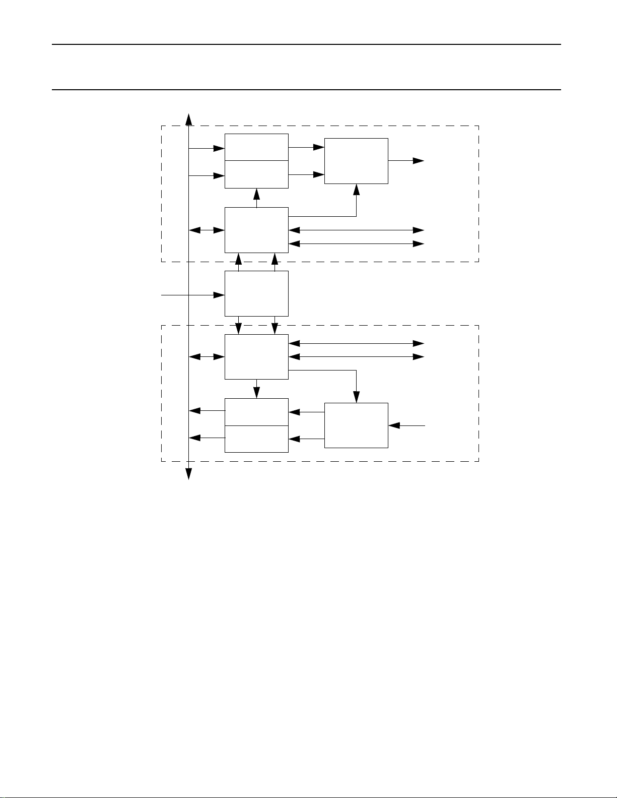
SERIAL PORT INTERFACES
OVERVIEW
2
The SAA7785 chip will contain an S/PDIF Consumer Grade transmit port and an I
ports are designed to exchange digital audio data but can be used for any type of data transfer assuming the bandwidth
is adequate. Currently, these ports are connected to the DSP data bus.
The Inter-IC Sound Bus, or I
interface is based on a continuous serial clock that determines the data rate along with the word select line and the data
lines. An I
2
S port can be a master or a slave device. A master device drives the serial clock and word select lines while
a slave device receives the clocking signals. The SAA7785 I
2
S Port, is a simple interface used to transfer digital data from one source to another. The
2
S ports are independently programmable to be either a
master or a slave and for 32.0, 44.1 and 48.0KHz stereo data transfer.
Also included is a Sony/Philips Digital Interface Format, or S/PDIF, serial port. This interface is generally used to trans -
mit raw audio data but is also used to transfer AC-3 encoded data as well using DMA. The S/PDIF format is a synchronous interface with the clock encoded on the data stream. The S/P DIF port s s upport 32.0, 44. 1 and 48.0K Hz stereo
data transfer up to 24 bits. The S/PDIF interface is IEC958 Consumer Grade compliant.
S transmit/receive pair. These serial
1999 Nov 12 15
Page 16
Philips Semiconductors Preliminary Specification
ThunderBird AvengerTM PCI Audio SAA7785
Accelerator
2
FIGURE 4 I
S SERIAL PORTS BLOCK DIAGRAM
CCLK
Right Data
Left Data
Transmit
Control
Logic
I2S Ports
Clock
Divider
Receive
Control
Logic
Left Data
Right Data
Transmit
Shift
Register
Receive
Shift
Register
XDATA
XSCLK
XWS
RWS
RSCLK
RDATA
DSP DATA BUS
1999 Nov 12 16
Page 17

Philips Semiconductors Preliminary Specification
ThunderBird AvengerTM PCI Audio SAA7785
Accelerator
FIGURE 5 S/PDIF TRANSMIT PORT BLOCK DIAGRAM
Audio Data
Holding
Registers
DSP DATA BUS
Aux Data
Holding
Registers
Ctl/Channel
Stat Holding
Registers
User Data
Holding
Register
S/PDIF XMT
Port Status
Register
Audio Data
Shift
Registers
Validity Bit
Generation
Aux Data
Shift
Registers
Ctl/Channel
Stat Shift
Registers
User Data
Shift
Register
MUX
Bi-Phase
Mark
Encoder
Line
Driver
SPDO
CCLK
DCLK
S/PDIF XMT
Control
Logic
S/PDIF XMT
Clock
Divider
Preamble
Generation
Parity
Generation
VIRTUAL WRITE MASTER
Audio streams may be directed back to host memory f rom t he DSP domain. The VWM has a data buffer capable of
storing enough audio data to burst into the host memory. The VWM is a simplified version of DMA and has more stringent requirements on which and how many pages need to be allocated.
Using the VWM, the system programmer can redirect audio streams processed by the SAA7785 ThunderBird Aveng-
TM
er
device and use them in any other audio device that resides in the system. The VWM is more efficient than the
DMA and should be the device of choice when redirecting audio streams back to the host. The device supports audio
sample rates from 8 to 48 KHz.
1999 Nov 12 17
Page 18

Philips Semiconductors Preliminary Specification
ThunderBird AvengerTM PCI Audio SAA7785
Accelerator
Game Port
The SAA7785 ThunderBird AvengerTM Game Port interface is designed to emulate the PC-AT based legacy joystick
operation as well as support of a digital joystick mode. The legacy or analog, type of operation is designed to support all
legacy software that uses the original joystick address and the method for resolving the joystick axes positions. The
Digital Mode is designed to reduce the joystick overhead by resolv ing the joyst ick pos ition directly and to support applications that use DirectInput.
The legacy joystick used a one shot multi-vibrator on each of the four joystick potentiometers. These one shots were
set up to deliver a pulse that was proportional to the resistor value of the joystick potentiometers. Software would them
poll the one shots to see if they had been set to the original value. The time it took for each axes to return to the original
value was resolved into a position by the legacy software. The SAA7785 ThunderBird Avenger
based one shot circuit to support legacy games that use the PC -AT joyst ick. The joystick button v alues were routed
directly to the system bus where only a decode was required to read the value of the button. Software would poll the
buttons as well. All button and joystick axes data is returned in a single byte wide register.
Game Port Legacy I/O Register
This register is the legacy mode register for the 558 based joystick. When in “analog” mode, this register is aliased to
respond to addresses at base + (0-7) . Reads fr om this regist er will poll the status of the joystick but tons and are used
to resolve the position. Writes to this register will discharge the external capacitors to emulate the 558 one shots. Software can then poll the joystick register bit to resolve eac h of the joys tick ax es positions by timing. The joystick butt on
register bits have meaning in both the digital and analog modes. The axes bits are only valid for analog mode.
TM
emulates the 558
TABLE 3 Game Port 558-Based Register - GAMEPORT (RO)
I/O GMBASED7D6D5D4D3D2D1D0
Offset 1h JOYB_2 JOYB_1 JOYA_2 JOYA_1 JOYB_Y JOYB_X JOYA_Y JOYA_X
POR Value 11110000
Bit Name R/W Function
7 JOYB_2 RO Joystick B button 2 stat us. The joyst ick butt on s tatus bits are cleared when
the respective joystick button is pressed.
6 JOYB_1 RO Joystick B button 1 status.
5 JOYA_2 RO Joystick A button 2 status.
4 JOYA_1 RO Joystick A button 1 status.
3 JOYB_Y RO Joystick B y-c oordinate. Can also be referred to as position 3.
2 JOYB_X RO Joystick B x-c oordinate. Can also be referred to as position 2.
1 JOYA_Y RO Joystick A y-c oordinate. Can also be referred to as position 1.
0 JOYA_X RO Joystick A x-c oordinate. Can also be referred to as position 0.
1999 Nov 12 18
Page 19

Philips Semiconductors Preliminary Specification
ThunderBird AvengerTM PCI Audio SAA7785
Accelerator
SAA7785 SIGNAL DEFINITIONS
PCI LOCAL BUS INTERFACE SIGNALS
AD[31:0] PCI Address/Data
AD[31:0] contains a physical byte address during the first clock of a PCI transaction, and data
during subsequent clocks.
When the SAA7785 is a PCI master, AD[31:0] are outputs during the address phase of a transaction. They are either inputs or outputs during the data phase, depending on the type of PCI
cycle in process.
When the SAA7785 is a PCI slave, AD[31:0] are inputs during the address phase. They are
either inputs or outputs during the data phase, depending on the type of PC I cycle in process.
C/BE#[3:0] PCI Bus Command and Byte Enables
C/BE#[3:0] defines the bus command during the first cloc k of a PCI transaction, and the byte
enables during subsequent clocks.
C/BE#[3:0] are outputs when the SAA7785 is a PCI bus master and inputs when it is a PCI bus
slave.
DEVSEL# PCI Bus Device Select
When the SAA7785 is a PCI bus master the SAA7785 uses DEVSEL# to determine whether a
master abort should occur if DEVSEL# is not sampled active by clock 5 of the transaction, or to
determine whether a cycle is to be aborted or retried when a target-initiated termination occurs.
When the SAA7785 is a PCI bus slave, DEVSEL# is an output which the SAA7785 drives LOW
during the second PCLK after FRAME# assert ion to the end of a transac tion if t he SAA7785 is
selected.
FRAME# PCI Bus Cycle Frame
When the SAA7785 is a PCI mas t er, FRAME# is an output which indicates the beginning of a
SAA7785-initiated bus transaction. While FRAME# is asserted data transfers continue. When
FRAME# is deasserted the transaction is in the final data phase.
When the SAA7785 is a PCI s lave, FRAME# is an input that initiates an I/ O, memory or c onfiguration register access if the SAA7785 is selected for the transaction. The SAA7785 latches the
C/BE#[3:0] and AD[31:0] signals on the PCLK edge on which it first samples FRAME# active.
IRDY# PCI Bus Initiator Ready
When the SAA7785 is a PCI mast er, IRDY # is an output which indicates the SA A7785’s ability
to complete the data phase of the current transaction. It is always asserted from the PCLK
cycle after FRAME# is asserted to the last clock of the transaction.
When the SAA7785 is a PCI slave, IRDY# is an input which causes the SAA7785 to hold-off
completion of a read or write cycle until sampled active.
1999 Nov 12 19
Page 20

Philips Semiconductors Preliminary Specification
ThunderBird AvengerTM PCI Audio SAA7785
Accelerator
STOP# PCI Bus Stop (Target Initiated Termination)
When the SAA7785 is a PCI mas t er, STOP# is an input which causes the SAA7785 t o complete, abort or retry the transfer, depending on the stat e of TRDY# and DEVS EL#.
When the SAA7785 is a PCI slave, it drives STOP# as active (LOW) to terminate or retry a
transaction.
TRDY# PCI Bus Target Ready
When the SAA7785 is a PCI master, TRDY# is an input which indicates the target agent’s ability to complete the data phase of the transaction. After initiation of a PCI bus transaction, the
SAA7785 inserts wait cycles until TRDY# is sampled active.
When the SAA7785 is a PCI slav e, it drives TRDY# act ive to indicate that the SAA7785 has
sampled the data from AD[31:0] during a write phase, or presented valid data on AD[31:0] during a read phase.
PAR PCI Bus Parity
When the SAA7785 is a PCI master, it drives PAR to reflect the correct value for even parity on
the AD[31:0] and C/BE#[3:0] buses one clock after the address phase and after each write data
phases.
When the SAA7785 is a PCI slav e, it drives PAR to ref lect t he correct value for even parity on
the AD[31:0] and C/BE#[3:0] buses one clock af ter completion of each read data phase.
PCREQ# PC/PCI DMA Request
This signal requests DMA series from an external chipset that supports PC/PCI protocols. The
SAA7785 chip asserts PCGNT# according to the desired DMA channel required by either the
SoundBlaster or AC97 interfaces. The requested channel is encoded serially on the PCGNT#
pin.
The SAA7785 will become the bus ow ner w hen it r ece ives an ass erted PCGNT# signal. This
handshaking is synchronous to PCLK.
PCGNT# PC/PCI DMA Grant
An asserted PCGNT# pin indicates that t he external P C/ PCI master arbiter has granted DMA
services to the encoded DMA channel to the requesting DMA agent on the SAA7785 chip.
REQ# PCI Bus Request
This signal controls the PCI bus arbitration between the SAA7785 chip and the PC I mas ter
arbiter. When REQ# is asserted, the SAA7785 indicates a desire to become the PCI bus owner.
The SAA7785 will become the bus owner when it rec eives an ass erted grant signals (GNT# is
LOW). This handshaking is synchronous to PCLK.
REQ# is three-stated while RST# is active.
1999 Nov 12 20
Page 21

Philips Semiconductors Preliminary Specification
ThunderBird AvengerTM PCI Audio SAA7785
Accelerator
GNT# PCI Bus Grant
An asserted GNT# pin indicates that the PCI master arbiter has granted bus ownership to the
SAA7785 chip.
INTA# PCI Bus Interrupt A
The interrupt output is a PCI compatible active low level sensitive interrupt. It is only used if the
SAA7785 is used in a non Common Architecture system. Otherwise it is tri-stated. I t is driven
low when any of the internal interrupts are asserted.
PERR# PCI Bus Parity Error
This signal indicates a data parity error for any cycle type other than a Special Cycle command.
PERR# is made active two clocks after the completion of the data phase which caused the parity error. This error signal may result in the generation of a non-maskable interrupt (NMI) or
other high priority interrupt sent to the CPU.
SERR# PCI Bus System Error
This signal indicates an address parity error, data parity errors on Special Cycle commands or
any other catastrophic system error. SERR# is an open-drain bidirectional pin which is driven
low for a single PCLK cycle by the agent reporting the error. This error may result in the generation of a non-maskable interrupt (NMI) or other high priority interrupt sent to the CPU.
IDSEL Initialization Device Select
IDSEL is used as a chip select during configuration register read and write operations. One
system board address line from AD[31:11] is used as IDSEL to select the SAA7785 configuration space in the SAA7785 chip when used on the PCI bus.
CLKRUN# PCI Bus Clock Run Request
The SAA7785 uses CLKRUN# according to the Mobile PCI protocol to start the PCI clock or
keep the clock running whenever an internal PCI device requires it .
PCLK PCI Bus Clock Input
PCLK is the PCI bus clock input. It is used to synchronize all PCI bus operations and typically
runs at 33MHz.
RST# PCI Bus Reset
An active low version of the system reset, this signal causes the PCI interface to return to the
idle states in all state machines and asynchronously three-states all PCI bus signals. All registers will be reset to their default values as well. The CODEC interface line should be all driven
inactive along with the external memory interface. This reset will assert the DSP reset.
PME# PCI Bus Power Management Event
Reserved.
1999 Nov 12 21
Page 22

Philips Semiconductors Preliminary Specification
ThunderBird AvengerTM PCI Audio SAA7785
Accelerator
PCI GENERAL PURPOSE I/O
PGPIO[7:0] PCI General Purpose Input/Outputs
These eight pins are used as controls or data to dev ices ex ternal to t he SAA7785 chip. Each
are independently controlled.
TEST INTERFACE/SERIAL CONFIGURATION PORT
NAND#/CFGDAT
TRI#/CFGCLK Tri-State Test Enable/Serial Configuration Clock
GAME PORT INTERFACE
JACX Joystick A X Axis
NAND Tree Test Enable/Serial Configuration Data
When this pin is pulled low and RST# is pulsed asserted, all output and I/O pins of the
SAA7785 will be forced into a three-state condition. Pulsed assertion of the RST# signal will
release the SAA7785 from this test mode.
If this pin is pulled high during PCI reset, then it is used to shift in PCI configuration data for the
Subsystem ID and the Subsystem Vendor ID in each of the PCI configuration headers present
in the SAA7785 chip. The Serial Configuration Port is a standard I
never be pulled low.
When this pin is pulled low and RST# is pulsed asserted, the SAA7785 will enter the parametric
NAND tree test mode. The details of the NAND tree test mode are described later in this document.
If this pin is pulled high during PCI reset, then this pin will supply the serial 400 KHz clock,
derived from OSC, to an external serial EEPROM. CFGCLK is used to synchronize the serial
configuration data.
This pin functions as an input for the joystick A X-position axis.
2
C interface. This line should
JACY Joystick A Y Axis
This pin functions as an input for the joystick A Y-position axis.
JBCX Joystick B X Axis
This pin functions as an input for the joystick B X-position axis.
JBCY Joystick B Y Axis
This pin functions as an input for the joystick B Y-position axis.
JAB2 Joystick A Button 2 Interface
This pin functions as an input for the joystick A button 2.
1999 Nov 12 22
Page 23

Philips Semiconductors Preliminary Specification
ThunderBird AvengerTM PCI Audio SAA7785
Accelerator
JAB1 Joystick A Button 1 Interface
This pin functions as an input for the joystick A button 1.
JBB2 Joystick B Button 2 Interface
This pin functions as an input for the joystick B button 2.
JBB1 Joystick B Button 1 Interface
This pin functions as an input for the joystick B button 1.
MIDI INTERFACE
MIDIIN MIDI Serial Data Input
This signal is part of the standard 2 wire MIDI interface. This input receives MIDI data at a rate
of 31.25Kbaud. Optical isolation is required.
MIDIOUT MIDI Serial Data Output
This signal is part of the standard 2 wire MIDI interface. This output transmits MIDI data at a
rate of 31.25Kbaud. Optical isolation is required.
AC’97 CODEC INTERFACE
SYNC AC’97 Codec Synchronization/Frame Output
This signal is used to frame the tag packet from the AC link des igner from the SAA7785 chip.
BIT_CLK AC’97 Data Bit Clock
This signal is used to clock synchronous data on the AC link interface.
SDATA_OUT AC’97 Serial Data Out
This is the time division multiplexed serial output data stream from the SAA7785 controller.
SDATA_IN0 AC’97 Serial Data In Port 0
This is the time division multiplexed serial input data stream from the primary external AC’97
codec.
SDATA_IN1 AC’97 Serial Data In Port 1
This is the time division multiplexed serial input data stream from the secondary external AC’97
codec.
1999 Nov 12 23
Page 24

Philips Semiconductors Preliminary Specification
ThunderBird AvengerTM PCI Audio SAA7785
Accelerator
AC_RST_N# AC’97 Master Reset
The external AC’97 codec has a master reset line which is has a separate control. The codec
status must report a ready before any audio or modem data is transmitted to t he codec .
DSP SERIAL PORTS/GENERAL PURPOSE I/O
SPDO Sony/Philips Digital Interface Format Output Port
Consumer format S/PDIF Output Port . The output characteristic of this pad approximates t he
RS422 interface.
SPDI Sony/Philips Digital Interface Format Input Port
Reserved.
RWS Inter-IC Sound Bus Receive Port Word Select Clock/DSP General Purpose I/O 0
When the I2S is configured as a master, this pin w ill output a w ord c lock at the frequency
selected by the user. When configured as a slave, the receive port will sync hronize t he left or
right channel data to this signal.
RSCK Inter-IC Sound Bus Receive Port Bit Clock/DSP General Purpose I/O 1
When the I2S is configured as a master, this pin will output a bit clock. When configured as a
slave, the receive port will shift in data from the RSD data stream using RSCK as an input.
RSD Inter-IC Sound Bus Receive Port Data/DSP General Purpose I/O 2
This pin is the input data stream for the I2S receive port.
TWS Inter-IC Sound Bus Transmit Port Word Select Clock
When the I2S is configured as a master, this pin w ill output a w ord c lock at the frequency
selected by the user. When configured as a slave, the receive port will sync hronize t he left or
right channel data to this signal.
TSCK Inter-IC Sound Bus Transmit Port Bit Clock
When the I2S is configured as a master, this pin will output a bit clock. When configured as a
slave, the transmit port will shift out data from the TSD data stream using TSCK as an input.
TSD Inter-IC Sound Bus Transmit Port Data
This pin is the output data stream for the I2S transmit port.
1999 Nov 12 24
Page 25

Philips Semiconductors Preliminary Specification
ThunderBird AvengerTM PCI Audio SAA7785
Accelerator
PLL/DSPCLK SUBSYSTEM INTERFACE
CCLK CODEC Clock Input
This pin is the raw 24.576MHz clock from the AC’97 crystal. The CCLK clock is used to provide
a fixed time base for many functions within the SAA7785 device.
DSPCLK DSP Clock Input
This pin can be used as the clock input for the SAA7785 for the DSP subsystem in place of the
PLL driving the clock. DSPCLK is also used to drive the DSP subsystem for controllability during testing.
PSUB PLL Substrate
This pin supplies the bias for the guard ring on the PLL core. Connect this to a clean analog
supply ground.
PLLAPWR PLL Analog Power
Analog power supply for the PLL. Be sure the analog supply is isolated from the 3 volt digital
supply.
PLLAGND PLL Analog Ground
Analog ground for the PLL. This power supply is sensitive to noise and should be handled carefully.
POWER AND GROUND PINS
VDDIC Core Power
3 volt power supply for the core of the chip.
VSSIC Core Ground
Ground reference for the core of the chip.
VSS Ring Ground
Ground reference for the pad interfaces of the chip.
VDD Ring Power
3 volt supply for the pad interfaces of the chip.
NWELL External N-Well Bias
Tie these pins to 5v for proper 5 volt tolerant operation. The 5v supply must be powered up
before the 3v supply. Likewise, the 3v supply must be powered down before the 5v supply.
PLEASE READ THE CAUTIONS IN Section 4.1, POWER SUPPLY OPERATING REQUIREMENTS ***** MUST REA D *****
1999 Nov 12 25
Page 26

Philips Semiconductors Preliminary Specification
ThunderBird AvengerTM PCI Audio SAA7785
Accelerator
DSP EXTERNAL MEMORY INTERFACE
MA[14:0] External Memory Address
Address lines for the external SRAM devices. The ext ernal memory interface c an be used for
DSP code space if the EXT_SRAM_EN (in HDCFG, bit 5) is set. Otherwise, the DS P will use
internal ROM as the code source.
MD[15:0] External Memory Data Bus
Word wide data bus for the external SRAM. Use 6ns memory for maximum DSP performance.
MCS# External Memory Chip Select
Chip select line for the external SRAM devices.
MWE# External Memory Read/Write Control
Selects the external SRAM for reading or writing.
1999 Nov 12 26
Page 27

Philips Semiconductors Preliminary Specification
ThunderBird AvengerTM PCI Audio SAA7785
Accelerator
SAA7785 ThunderBird Avenger™ Functional Block Descriptions
Register Table Document Description and Example
The next table gives an example of how registers are documented in this spec ification.
TABLE 4 Example Register - REGEX (RW/RO)
SPACE D15 D14 D13 D12 D11 D10 D9 D8
Offset nnh RRRRRRRR
POR Value 00000000
D7 D6 D5 D4 D3 D2 D1 D0
EXDATA[7:0]
POR Value 00000000
Bit Name R/W Function
15:8 R RO Reserved. These bits always return zeros.
7:0 EXDATA RW Example data. The example data for all to see.
In the above table example, the EXAMPLE RE GIS TER tex t would be a descriptive title for the register that we wish t o
detail. Following the register description would be a register mnemonic used in register summary tables and the like. In
this example the mnemonic is REGEX. Following the mnemonic is the read/write access allowed into this register. If the
entire register is readable and writable, then the RW key is assigned. If some bits are read/write while others are read
only, then the key will indicate this fact. In the example, this register has both read/write and read only bits. The register
memory map location is marked in the table cell marked SPACE. SPACE could be substituted with PCI CFG n (for PCI
configuration re giste r sp a ce fo r fu n ctio n n ), IOBASE ( fo r a n I/O sp a ce r e g ister with a n IOBASE spe cified in a co n fig u r a tion register), DSP DATA (for DSP data memory mapped registers), MEM MSTR (indicating a PCI master in memory
space), and DSP CODE (indicating a DSP code memory mapped register. Just below the S PACE marker is the offset
from the base address spec ified in the SPACE field. The rest of the table should be obvious.
SAA7785 ThunderBird Avenger™ PCI Interface
Overview
The SSA7785 ThunderBird Avenger™ chip PCI interface is designed to interface the external PCI bus interface to all of
the selected devices in the SSA7785 ThunderBird Avenger™ chip. The PCI interfac e composed of mas ter and slave
state machines, an address/data/byt e enable datapath, a bus arbiter for the two on c hip masters, cont rol logic for the
master and slave internal busses, and standard PCI configuration register headers. The Interrupt S erializer will be discussed in a later chapter. This section of the s pec ification w ill desc ribe the PCI interfac e in more detail along with
design considerations for both the slave, master, and datapath. The configuration header will be discussed in the
SSA7785 ThunderBird Avenger™ PCI Configuration Registers sect ion of this specificat ion.
The discussion will begin with the PCI master and target systems. The PCI bus master has the capability to burst double words to/from the two internal bus masters, the Distributed DMA and the Virtual Registers. The full address range is
supported for these master devices. S ince there are two masters, an arbit er is required to determine priority between
the two devices. Details on the arbiter can be found in the PCI master section.
1999 Nov 12 27
Page 28

Philips Semiconductors Preliminary Specification
ThunderBird AvengerTM PCI Audio SAA7785
Accelerator
The PCI datapath block contains the multiplexors and registers to steer the data to and from the PCI interfaces. The
data is de-multiplexed from the external PCI interface t o t he internal master and slave busses . Control logic from the
master and slave devices control the datapath.
The SSA7785 ThunderBird Avenger™ is considered a multi-function device since the operating system may wish to
load different drivers for certain functions. These functions are the audio subsystem, the joyst ick and the 16650 UART.
Each of these major functions must have a separate PCI configuration space. The standard PCI configuration header
for these three functions are supported in the PCI interf ace.
The SSA7785 ThunderBird Avenger™ PCI interface responds to and initiates PCI cycles with positive decoding
according to the PCI 2.1 specification. The interface asserts DEVSEL# after the first clock following FRAME# making it
a medium responder. For specific LAM cycles, the SSA7785 ThunderBird Avenger™ will be a fast responder. SSA7785
ThunderBird Avenger™ indicates which cycles the PCI interface responds to or initiates.
TABLE 5 PCI Bus Command Definitions and SSA7785 ThunderBird Avenger™ Responses
c/be#[3:0] Command Type SSA7785 ThunderBird Avenger™ Response to Cycle
0000 Interrupt Acknowledge This cycle is not claimed.
0001 Special Cycle This cycle is not claimed.
0010 I/O Read All I/O Read cycles directed to the SSA7785 ThunderBird
Avenger™ are claimed by the target interface.
0011 I/O Write All I/O Write cycles directed to the SSA7785 ThunderBird
Avenger™ are claimed by the target interface.
0100 Reserved This cycle is not claimed.
0101 Reserved This cycle is not claimed.
0110 Memory Read This cycle is not claimed.
0111 Memory Write This cycle is not claimed.
1000 Reserved This cycle is not claimed.
1001 Reserved This cycle is not claimed.
1010 Configuration Read All Configuration Read cycles are claimed by the target interface
provided IDSEL is sampled asserted during the address/cmd
phase.
1011 Configuration Write All Configuration Write cycles are claimed by the target interface
provided IDSEL is sampled asserted during the address/cmd
phase.
1100 Memory Read Multiple This cycle is not claimed.
1101 Dual Address Cycle The SSA7785 ThunderBird Avenger™ supports 32-bit
addresses only.
1110 Memory Read Line This cycle is not claimed.
1111 Memory Write and Invalidate This cycle is not claimed.
The SSA7785 ThunderBird Avenger™ will res pond to byte, w ord, tri-by te or double w ord acce ss for configuration read
and configuration write cycles provided PCI addressing rules are followed. Byte and word width accesses allowed for
I/O cycles depend largely on the target I/O device. In general, 24-bit and 32-bit accesses are not allowed to I/O devices
and will result in a target abort. The SSA7785 ThunderBird Avenger™ performs double word accesses when initiating
1999 Nov 12 28
Page 29

Philips Semiconductors Preliminary Specification
ThunderBird AvengerTM PCI Audio SAA7785
Accelerator
master cycles. Note that the SSA7785 ThunderBird Avenger™ cannot initiate a master cycle to itself. SSA7785 ThunderBird Avenger™ summarizes the access rules for configuration and I/O c ycles .
TABLE 6 BIT Width Device Access Rules
Data
Device Cycle Types
Width Comments
PCI Configuration
Registers
Game Port I/O Read
AC’97 Codec I/O Read
DMA Interface I/O R/W Any
Sound Blaster Regis-
ters
Virtual Registers Mem Read Any Follow PCI addressing rules.
Host/DSP Interface I/O Read
MPU401 Registers I/O Read
Config Read
Config Write
I/O Write
I/O Write
I/O Read
I/O Write
I/O Write
I/O Write
Any Follow PCI addressing rules, otherwise assert a target abort.
Note that configuration registers, no matter where they are,
are accessed by configu ration cycles o nly. Note th at the PLL
will only allow 8 bit configuration accesses, the Virtual Registers TBLBASE registers are 32 b it acce ss o n ly, and th e
VRCFG is 16 bit access only.
8 Any other access will result in a target abort.
16 For PIO type accesses, only 16 bit I/O cycles are allowed,
other wise a target abort will result.
8 Any other access will result in a target abort.
8,16 Usually, only 16 bit accesses will be us ed to download and
access the DSP. Byte wide are also allowed for DSP configuration accesses. Word accesses must be on word boundaries.
8 Any other access will result in a target abort.
16650 UART I/O Read
I/O Write
The PCI interface consists of t hree major blocks, the P CI master interface, the P CI slave interface and the PCI datapath. The PCI master interface contains the master state machine, the master control logic, and the PM bus arbiter. The
PCI slave interface contains the target state machine, the target control logic and configuration register headers. The
PCI datapath is the de-multiplexing logic for the address, data and byte enable data paths for the PS and PM busses.
The PM and PS busses are described in detail in the SSA7785 ThunderBird Avenger™ Internal Busses section. Partitioning of these PCI blocks are done in this manner to reduce block inter-connectivity and to provide an interface
between the three major sections of the PCI interface.
PCI Master Interface
The SSA7785 ThunderBird Avenger™ PCI master interface performs the memory read and write cycles initiated by the
DMA or Virtual Registers blocks. The major components of the PCI master interface are the master state machine, the
PM bus arbiter and the master control logic. Each of the functional blocks will be discussed in detail.
1999 Nov 12 29
8 Any other access will result in a target abort.
Page 30

Philips Semiconductors Preliminary Specification
ThunderBird AvengerTM PCI Audio SAA7785
Accelerator
PCI Master State Machine
This block will performs the handshaking between the PCI interface and t he PM internal bus. The PCI mast er will perform bursting in a linear incrementing type fashion. The PCI master state machine may also wish to provide a target
lockout signal. This signal prevents the PCI target interface fr om responding to any master s ignals.
PC/PCI Legacy Support
The PCI block supports the PC/PCI sideband signals for legacy support of the soundblaster. The PC/PCI can be
enabled by a configuration register bit and one channel selected. The PCI s lave block will provide the serial encoded
request signal (PCREQ#) in response to a request from the soundblaster and decode the serial encoded PCGNT# line.
The PCI slave will then claim I/O writes to addres s 0000h or 0004h with the PCGNT# line asserted as writes to the
SoundBlaster and pass the data to the SoundBlaster.
PCI Target State Machine
The PCI target state machine controls all SSA7785 ThunderBird Avenger™ target responses on the PCI bus in addition
to handling the PS internal bus.
PCI Target Control Logic
The target control logic handles the address decoding for the ps_NNNcs# signals, bus command decoding for the
ps_XXXrd# and ps_XXXwr# signals, determination of target abort conditions, and data path/pad control logic from the
target interface. Also included in this logic are the controls for the PCI datapath and I/O pads. These controls are sent to
the datapath logic where they are combined with the mas ter cont rols and then sent t o the datapat h and pad devices.
The control logic also includes an interface to the PCI c onfiguration headers.
Serial Configuration Port
The Subsystem Vendor ID and Subsystem ID for each of the configuration headers presents a special case. These
three 32 bit registers must be programmed by the Subsystem Vendor. It is impractical to hard wire the Subsystem ID
registers since each Subsystem Vendor will hav e a unique ID. Therefore an ex ternal serial EEROM device is used to
download the proper values into the ID registers after reset and before begin read by t he BIOS or other conf iguration
software. The PCI interface should f orce a retry if any of the s ubsy stem registers have not completed a loading. The
Serial Configuration Port is a standard two pin I
the external serial EEPROM on the CFGCLK pin. The serial data stream will arrive on the CFGDAT input pin. Please
refer to a 24LC00 128 bit I
2C
Bus Serial EEPROM data sheet for interface protocols and timings.
2
C interface. The ThunderBird Q3DIII will supply the 400 KHz clock to
Serial Configuration Port Programming
The SSA7785 ThunderBird Avenger™ uses an inexpensive external EEPROM, programmed before installation, to
download the Subsystem Vendor ID and Subsystem ID registers for each function for a total of 96 bits (six 16 bit registers). The recommended device, a Microchip 24LC01B 1K Bit (128 Byte) Serial EEPROM, can be programmed using a
conventional DATA I/O programmer.
CFGDAT
ThunderBird
CFGCLK
1999 Nov 12 30
SDA
EEPROM
SCL
+5V
WP
Page 31

Philips Semiconductors Preliminary Specification
ThunderBird AvengerTM PCI Audio SAA7785
Accelerator
FIGURE 6
In each of the three SSA7785 ThunderBird Avenger™ functions PCI configuration space there is a Subsystem Vendor
ID register at an offset of 2Ch and a Subsystem ID register at an offset of 2Eh. E ach register is 16 bits in length and is
write-only by the serial EEPROM and read-only from the PCI interface. The data from the EEPR OM is loaded into the
registers immediately after PCI reset. If no EEPROM is detected, the default values are loaded and shown in SSA7785
ThunderBird Avenger™ and reflect the default values for the System ID and Vendor ID for that function.
TABLE 7 Subsystem Register Default Values
Function Device Type Offset Register Name Default Value
0 Audio Subsystem 2Ch Subsystem Vendor ID 1004h
0 Audio Subsystem 2Eh Subsystem ID 0304h
1 Joystick 2Ch Subsystem Vendor ID 1004h
1 Joystick 2Eh Subsystem ID 0305h
2 16650 UART 2Ch Subsystem Vendor ID 1004h
2 16650 UART 2Eh Subsystem ID 0306h
The EEPROM contains bits 000h through 3FFh. Only bits 000h through 05Fh are utilized to program the Subsystem ID
and Subsystem Vendor ID registers . The bit assignments between the EEPROM and the configuration registers are
shown in SSA7785 ThunderBird Avenger™.
TABLE 8 EEPROM BIT Assignments to Subsystem Registers
Function 0 - Audio Subsystem Function 1 - Joystick Function 2 - 16650 Modem UART
Subsystem Vendor
ID - Offset 2Ch
EEPROM
Bit #
000h 15 010h 15 020h 15 030h 15 040h 15 050h 15
001h 14 011h 14 021h 14 031h 14 041h 14 051h 14
002h 13 012h 13 022h 13 032h 13 042h 13 052h 13
003h 12 013h 12 023h 12 033h 12 043h 12 053h 12
004h 11 014h 11 024h 11 034h 11 044h 11 054h 11
005h 10 015h 10 025h 10 035h 10 045h 10 055h 10
006h 9 016h 9 026h 9 036h 9 046h 9 056h 9
007h 8 017h 8 027h 8 037h 8 047h 8 057h 8
008h 7 018h 7 028h 7 038h 7 048h 7 058h 7
009h 6 019h 6 029h 6 039h 6 049h 6 059h 6
00Ah 5 01Ah 5 02Ah 5 03Ah 5 04Ah 5 05Ah 5
00Bh 4 01Bh 4 02Bh 4 03Bh 4 04Bh 4 05Bh 4
00Ch 3 01Ch 3 02Ch 3 03Ch 3 04Ch 3 05Ch 3
00Dh 2 01Dh 2 02Dh 2 03Dh 2 04Dh 2 05Dh 2
00Eh 1 01Eh 1 02Eh 1 03Eh 1 04Eh 1 05Eh 1
Reg
Bit #
Subsystem ID -
Offset 2Eh
EEPROM
Bit #
Reg
Bit #
Subsystem Vendor
ID - Offset 2Ch
EEPROM
Bit #
Reg
Bit #
Subsystem ID -
Offset 2Eh
EEPROM
Bit #
Reg
Bit #
Subsystem Vendor
ID - Offset 2Ch
EEPROM
Bit #
Reg
Bit #
Subsystem ID -
Offset 2Eh
EEPROM
Bit #
Reg
Bit #
1999 Nov 12 31
Page 32

Philips Semiconductors Preliminary Specification
ThunderBird AvengerTM PCI Audio SAA7785
Accelerator
Function 0 - Audio Subsystem Function 1 - Joystick Function 2 - 16650 Modem UART
Subsystem Vendor
ID - Offset 2Ch
EEPROM
Bit #
00Fh 0 01Fh 0 02Fh 0 03Fh 0 04Fh 0 05Fh 0
Reg
Bit #
Subsystem ID -
Offset 2Eh
EEPROM
Bit #
Reg
Bit #
Subsystem Vendor
ID - Offset 2Ch
EEPROM
Bit #
Reg
Bit #
Subsystem ID -
Offset 2Eh
EEPROM
Bit #
Reg
Bit #
Subsystem Vendor
ID - Offset 2Ch
EEPROM
Bit #
Reg
Bit #
Subsystem ID -
Offset 2Eh
EEPROM
Bit #
Reg
Bit #
These bits correspond to Function 0, Subsystem ID (off set 2Eh) bits 2, 1, and 0, respec tively. The Vendor should
choose and ID that corresponds to the peripherals present and program t he EEPROM ac cordingly.
PCI Datapath
The PCI datapath provides the flip flops to convert the external PCI interface address, data, command and byte enables
busses to the internal PM and PS bus ses.
PCI Configuration Register
Since the SSA7785 ThunderBird Avenger™ is a multi-function device, there are three configuration headers. They are
defined as the audio configuration header as function 0, the joystick configuration header as function 1, and the UART
configuration header defined as function 2. Eac h conf iguration spac e is divided up into two groups, the registers that
stay with the PCI interface and the registers that do not. This section will describe the PCI configuration registers that
bunk with the PCI interface. These registers include the PC I s tandard c onfiguration header registers and the base
address registers for various blocks in the SSA7785 ThunderBird Avenger™ chip.
To be more specific, the registers in the offset config space from 00h - 3Fh are the predefined PCI configuration header.
All three PCI co nfig ur atio n header reg ister s will r e side with the PCI inte rfa ce. The remainder of the re giste rs a re fun ction specific and can be found in the block section itself.
The following sections will detail each of the configuration header spaces for each of the SSA7785 ThunderBird
Avenger™ functions: audio, joystick and UART.
PCI Configuration Space 0
The following table is a summary of all the PCI configuration space registers. The registers that are block-mates with
the PCI interface (offset 00h - 44h) will be detailed following SSA7785 ThunderBird Avenger™. The remainder of the
registers will be detailed with the blocks they control.
TABLE 9 PCI Configuration Space 0 Register Map
Byte 3 Byte 2 Byte 1 Byte 0 Offset
Device ID Vendor ID 00h
Status Command 04h
Class Code Revision ID 08h
BIST Header Type Master Latency Timer Cache Line Size 0Ch
SONGBASE 10h
SBBASE 14h
MDBASE 18h
ALBASE 1Ch
Reserved 20-2Bh
1999 Nov 12 32
Page 33

Philips Semiconductors Preliminary Specification
ThunderBird AvengerTM PCI Audio SAA7785
Accelerator
SUBSYSTEM ID SUBSYSTEM VENDOR ID 2Ch
Reserved 30-3Bh
Max_Lat Min_Gnt Interrupt Pin Interrupt Line 3Ch
DMABBASE DMAABASE 40h
Reserved 44-57h
Reserved Reserved Reserved MSCCFG 58h
Reserved Reserved Reserved ACLCFG0 5Ch
Reserved Reserved VRCFG 60h
Reserved Reserved Reserved TIMRCFG0 64h
Reserved Reserved HDCFG 68h
Reserved 6Ch
Reserved Reserved DMACFG 70h
Reserved 74-77h
Reserved Reserved Reserved DPLLCTL0 78h
Reserved Reserved Reserved DPLLCTL1 7Ch
Reserved Reserved Reserved DPLLCTL2 80h
Reserved 84-87h
Reserved Reserved Reserved TESTCTL0 88h
Reserved 8C-8Fhh
TBLBASE0 90h
TBLBASE1 94h
TBLBASE2 98h
TBLBASE3 9Ch
Reserved Reserved Reserved IRQCTL0 A0h
Reserved Reserved Reserved IRQCTL1 A4h
Reserved Reserved Reserved IRQCTL2 A8h
Reserved Reserved Reserved IRQCTL3 ACh
Reserved Reserved Reserved IRQCTL4 B0h
Reserved Reserved Reserved IRQCTL5 B4h
Reserved Reserved Reserved IRQCTL6 B8h
Reserved Reserved Reserved IRQCTL7 BCh
Reserved Reserved Reserved COMARCH0 C0h
Reserved C4-EFh
DMAACCNT DMAACADR F0h
DMABCCNT DMABCADR F4h
DMAMASK DMACMD DMAAMODE Reserved F8h
Reserved Reserved DMABMODE Reserved FCh
TABLE 10 Vendor ID Register - VENDOR_ID (RO)
PCI CFG 0 D15 D14 D13 D12 D11 D10 D9 D8
Offset 00h
POR Value
00010000
VENDOR_ID[15:8]
1999 Nov 12 33
Page 34

Philips Semiconductors Preliminary Specification
ThunderBird AvengerTM PCI Audio SAA7785
Accelerator
D7 D6 D5 D4 D3 D2 D1 D0
VENDOR_ID[7:0]
POR Value
Bit Name R/W Function
15:0 VENDOR_ID RO The PCI Vendor ID for Philips Semiconductors (V LSI) is 1004h.
TABLE 11 Device ID Register - DEVICE_ID (RO)
PCI CFG 0 D15 D14 D13 D12 D11 D10 D9 D8
Offset 02h
POR Value
POR Value
Bit Name R/W Function
15:0 DEVICE_ID RO The Device ID for the SSA7785 ThunderBird Avenger™, function 0 is 0304h.
00000100
DEVICE_ID[15:8]
00000011
D7 D6 D5 D4 D3 D2 D1 D0
DEVICE_ID[7:0]
00000100
TABLE 12 Command Register - COMMAND (RO/RW)
PCI CFG 0 D15 D14 D13 D12 D11 D10 D9 D8
RRRRRRFBACK_
Offset 04h
POR Value
POR Value
Bit Name R/W Function
15:10 R RO Reserved. These bits always return zero.
1999 Nov 12 34
00000000
D7 D6 D5 D4 D3 D2 D1 D0
STEP-
PING
00000000
PERR_
RESP
SNOOP_
ENB
MEM_
INV_EN
SPEC_
CNTL
MAST_
CNTL
ENB
MEM_
CNTL
SERR_R
ESP
IO_
CNTL
Page 35

Philips Semiconductors Preliminary Specification
ThunderBird AvengerTM PCI Audio SAA7785
Accelerator
Bit Name R/W Function
9 FBACK_ENB RO Fast Back-to-Back Enable: the SSA7785 ThunderBird Av enger™, f unc tion 0
does not support fast back to back master cy cles therefore this bit always
returns a zero.
8 SERR_RESP RW System Error Response: When set to 1, the SSA7785 ThunderBird
Avenger™, function 0 responds to detected PCI bus address parity errors by
asserting SERR#. When 0, the SSA7785 ThunderBird Avenger™ ignores
these errors.
7 STEPPING RO Address / Data St epping: Always returns 0.
6 PERR_RESP RW Parity Error Response: When set to 1, the SSA7785 ThunderBird Avenger™,
function 0 responds to detected PCI bus data parity errors by asserting
PERR#. When 0, the SSA7785 ThunderBird Avenger™ ignores PCI bus data
parity errors.
5 SNOOP_ENB RO VGA Snoop Enable. The SSA7785 ThunderBird Avenger™, function 0 does
not support VGA snoop enable, therefore this bit always returns a zero.
4 MEM_INV_EN RO Memory Write and Invalidate Enable: Always returns 0.
3 SPEC_CNTL RO Special Cycle Control: Controls the devices ability to respond to Special
Cycle Operations. A value of 0 causes the SSA7785 ThunderBird Avenger™,
function 0 to ignore all Special Cycles.
2 MAST_CNTL RW Master Control: Controls the devices ability to act as a master on the PCI bus.
A value of 0 disables the ability of the SSA7785 ThunderBird Avenger™,
function 0, to act as a primary PCI master. A value of 1 enables the Thunder-
Bird Q3DIII, function 0 to become a PCI bus master.
1 MEM_CNTL RO Memory Response Control: The SSA7785 ThunderBird Avenger™, function 0
does not support target memory cycles therefore this bit always returns a
zero.
0 IO_CNTL RW I/O Response Control: Controls the SSA7785 ThunderBird Avenger™, func-
tion 0’s response to I/O space. A value of 0 disables the dev ice respons e. A
value of 1 allows the device to respond to I/O space accesses.
TABLE 13 Status Register - Status (RO/RW)
PCI CFG 0 D15 D14 D13 D12 D11 D10 D9 D8
R_PERR S_SERR SM_
Offset 06h
POR Value
00000010
ABORT
RT_
ABORT
ST_
ABORT
DEVSEL_TMG S_PERR
D7 D6 D5 D4 D3 D2 D1 D0
F_
BK2BK
POR Value
1999 Nov 12 35
10000000
UDFMHz66RRRRR
Page 36

Philips Semiconductors Preliminary Specification
ThunderBird AvengerTM PCI Audio SAA7785
Accelerator
Bit Name R/W Function
15 R_PERR RC Received P arity E rror: When set t o 1, this bit indicates that the SSA 7785
ThunderBird Avenger™, function 0 has detected a PCI bus parity error at
least once since this bit was last reset.
14 S_SERR RC Signalled System Error: When s et t o 1, this bit indicates that the SSA7785
ThunderBird Avenger™, function 0 has reported a system error on the
SERR# signal at least once since this bit was last reset.
13 SM_ABORT RC Signalled Master Abort: When set to 1, this bit indicates that the SSA7785
ThunderBird Avenger™, function 0 (acting as a master) had to initiate a mas-
ter abort at least once since this bit was last reset.
12 RT_ABORT RC Received Target Abort: When set to 1, this bit indicates that the SSA7785
ThunderBird Avenger™, function 0 (acting as a master) has received a target
abort at least once since this bit was last reset.
11 ST_ABORT RC Signalled Target Abort: When s et t o 1, this bit indicates that the SSA7785
ThunderBird Avenger™, function 0 has signalled a target abort at least once
since this bit was last reset.
10:9 DEVSEL_TMGRO DEVSEL Timing: This field indicates the timing of the DEVSEL output (when
a PCI master is accessing a SSA7785 ThunderBird Avenger™, function 0
resource). It always returns 01 (Bin).
00 = Fast
01 = Medium (Default Timing)
10 = Slow
8 S_PERR RC Signalled Parity Error: When set to 1, this bit indicates that the SSA7785
ThunderBird Avenger™, function 0 was a bus master for a cycle in which
PERR# was activated. This bit cannot be set if the PERR_RESP bit in the
command register is not enabled.
7 F_BK2BK RO Always returns 1 to indicate support of fast back to back cyc les when the
SSA7785 ThunderBird Avenger™, function 0 is the target.
6 UDF RO User Definable Features. Always returns 0.
5 MHz66 RO 66 MHzMHz Capable. Always returns 0.
4:0 R RO Reserved. These bits always return zero.
Note: An RC indicates that this bit can be reset to 0 by writing a 1. Writing a zero leaves this bit unchanged.
TABLE 14 Revision ID Register - REVISION (RO)
PCI CFG 0D7D6D5D4D3D2D1D0
Offset 08h
REVISION_ID[7:0]
POR Value
1999 Nov 12 36
00011001
Page 37

Philips Semiconductors Preliminary Specification
ThunderBird AvengerTM PCI Audio SAA7785
Accelerator
Bit Name R/W Function
7:0 REVISION_ID RO The current revision ID for the SSA7785 ThunderBird Avenger™, function 0,
the audio subsystem.
TABLE 15 Class Code Register - CLASS (RO)
PCI CFG 0 D23 D22 D21 D20 D19 D18 D17 D16
Offset 09h
POR Value
POR Value
POR Value
Bit Name R/W Function
23:16 BASE_CLASS RO The base class of 04h describes a PCI multimedia device.
15:8 SUB_CLASS RO The sub class of 01h describes a PCI audio multimedia device.
00000100
D15 D14 D13 D12 D11 D10 D9 D8
00000001
D7 D6 D5 D4 D3 D2 D1 D0
00000000
BASE_CLASS[7:0]
SUB_CLASS[7:0]
PGM_IFACE[7:0]
7:0 PGM_IFACE RO Device generic function identification.
TABLE 16 CACHELINE Size Register - CACHELINE (RO)
PCI CFG 0D7D6D5D4D3D2D1D0
Offset 0Ch
POR Value
Bit Name R/W Function
7:0 CACHELINE RO Reserved for cache line size indicator.
1999 Nov 12 37
00000000
CACHELINE[7:0]
Page 38

Philips Semiconductors Preliminary Specification
ThunderBird AvengerTM PCI Audio SAA7785
Accelerator
TABLE 17 Master Latency Timer Register - LATIME (RW)
PCI CFG 0D7D6D5D4D3D2D1D0
Offset 0Dh
POR Value
Bit Name R/W Function
7:0 LATIME RW The primary bus latency timer specifies the number of pr imary clocks that the
TABLE 18 Header Type Register - HEADER (RO)
PCI CFG 0D7D6D5D4D3D2D1D0
Offset 0Eh
POR Value
00000000
primary master may consume. The timer is reloaded at each assertion of
FRAME# by the primary master. If the primary master loses its bus grant,
then it must relinquish the bus after the timer expires.
MULTI_
FN
10000000
LATIME[7:0]
HEADER[6:0]
Bit Name R/W Function
7MULTI_FNROA 1 indicates that the SSA7785 ThunderBird Avenger™ is a multi-function
device. The three PCI configuration headers are accessed by the c onf iguration cycle address bits 10-8. The function definitions are as follows:
0 = Audio Subsystem
1 = Joystick
2 = 16650 UART
6:0 HEADER RO Header Type. A 00h indicates this device is a not a PCI-to-PCI bridge.
TABLE 19 BIST Register - BIST (RO)
PCI CFG 0D7D6D5D4D3D2D1D0
Offset 0Fh
POR Value
Bit Name R/W Function
7 BIST RO BIST capable. BIST is not supported in the SSA 7785 ThunderBird
BIST START R R CODE[3:0]
00000000
Avenger™, function 0 at this revision. It may be desired to include a BIST test
for the DSP at a later time.
1999 Nov 12 38
Page 39

Philips Semiconductors Preliminary Specification
ThunderBird AvengerTM PCI Audio SAA7785
Accelerator
Bit Name R/W Function
6 START RO If BIST capable, this bit w ill star t the BIST. Writing a 1 will s tart the test and
the BIST should write this bit to a zero when c omplete. Sof tw are should fail
the device if the BIST is not complete after 2 seconds.
5:4 R RO Reserved. These bits always return zero.
3:0 CODE RO Completion Code. A value of zero means the device has passed its test.
Non-zero values means the device has failed using device specific f ailure
codes.
SSA7785 ThunderBird Avenger™ CFG Space 0 Non-Legacy Base Address Registers
The Thunderbird Base Address Register (SONGBASE) is used to I/O map all of the non-legacy I/O devices in the
SSA7785 ThunderBird Avenger™ chip. The SONGBASE register maps the two DMA channels, the AC Link registers,
the Host/DSP interface, t he Serial Port interfaces, and the Multimedia Timer. The offset index for each of t he devices
are shown below: SSA7785 ThunderBird Avenger™ Non-Legacy I/O Device Map
Device Name Byte 3 Byte 2 Byte 1 Byte 0
TMCOUNT2 TMCOUNT1 TMCOUNT0 TMSTAT
Multimedia Timer
Reserved Reserved Reserved Reserved
Reserved Reserved Reserved Reserved
Reserved Reserved Reserved Reserved
Reserved Reserved
Serial Ports
Reserved Reserved
Reserved Reserved
Reserved Reserved
HDPCTL HDDATA
HDDLA HDPSTT
Host/DSP Interface
Reserved HDDLD
Reserved Reserved
ACDATA ACADDR
AC Link Interface
ACSTAT ACCTRL
ACPCML
ACPCMR
Serial IRQ Reserved Reserved Reserved IRQCTL
Thunderbird Reserved Reserved
Offset
00h
04h
08h
0Ch
10h
14h
18h
1Ch
20h
24h
28h
2Ch
30h
34h
38h
3Ch
40h
44-7Fh
TABLE 20 ThunderBird Base Address Register - Songbase (RW/RO)
PCI CFG 0 D31 D30 D29 D28 D27 D26 D25 D24
Offset 10h
POR Value
00000000
SONGBASE[31:24]
1999 Nov 12 39
Page 40

Philips Semiconductors Preliminary Specification
ThunderBird AvengerTM PCI Audio SAA7785
Accelerator
D23 D22 D21 D20 D19 D18 D17 D16
SONGBASE[23:16]
POR Value
POR Value
POR Value
Bit Name R/W Function
31:7 SONGBASE RW Thunderbird non-legacy device base address register. This register supplies
6:1 R RO Reserved. These bits are reserved a must always return a zero for plug and
0 IO RO I/O flag. This read only bit indicates that this is an I/ O range.
00000000
D15 D14 D13 D12 D11 D10 D9 D8
SONGBASE[15:8]
00000000
D7 D6 D5 D4 D3 D2 D1 D0
SONG
BASE[7]
00000001
RRRRRRIO
the I/O base address for the non-legacy I/O devices within the SSA7785
ThunderBird Avenger™ chip.
play.
SSA7785 ThunderBird Avenger™ CFG Space 0 Legacy Base Address Registers
The SSA7785 ThunderBird Avenger™ contains three legacy I/O base registers in configuration space 0. These legacy
devices are the Sound Blaster register, the AdLib registers and the MIDI interface registers. They are described in detail
in the next three tables.
TABLE 21 Sound Blaster Base Address- SBBASE (RW/RO)
PCI CFG 0 D31 D30 D29 D28 D27 D26 D25 D24
Offset 14h
POR Value
POR Value
1999 Nov 12 40
00000000
D23 D22 D21 D20 D19 D18 D17 D16
00000000
SBBASE[31:24]
SBBASE[23:16]
Page 41

Philips Semiconductors Preliminary Specification
ThunderBird AvengerTM PCI Audio SAA7785
Accelerator
D15 D14 D13 D12 D11 D10 D9 D8
SBBASE[15:8]
POR Value
POR Value
Bit Name R/W Function
31:4 SBBASE RW Sound Blaster programmable base address. The address should be on a 16 byte
3:1 R RO Reserved. These bits are reserved and always return zeros for plug and play.
0 IO RO I/O flag. This read only bit indicates that this is an I/ O range.
TABLE 22 MIDI Base Address- MDBASE (RW/RO)
PCI CFG 0 D31 D30 D29 D28 D27 D26 D25 D24
00000000
D7 D6 D5 D4 D3 D2 D1 D0
SBBASE[7:4] R R R IO
00000001
boundary. For reference, the Sound Blaster legacy base addresses are 220h and
240h. Note that accesses from the AdLib base address are mapped into a subset
of the SoundBlaster registers.
Offset 18h
POR Value
POR Value
POR Value
POR Value
MDBASE[31:24]
00000000
D23 D22 D21 D20 D19 D18 D17 D16
MDBASE[23:16]
00000000
D15 D14 D13 D12 D11 D10 D9 D8
MDBASE[15:8]
00000000
D7 D6 D5 D4 D3 D2 D1 D0
MDBASE[7:2] R IO
00000001
1999 Nov 12 41
Page 42

Philips Semiconductors Preliminary Specification
ThunderBird AvengerTM PCI Audio SAA7785
Accelerator
Bit Name R/W Function
31:2 MDBASE RW MIDI port programmable base address. The address should be on a double word
boundary. For reference the MIDI port legacy base addresses are 220h, 230h,
240h, 250h, 300h, 320h, 330h, 332h, 334h, 336h, 340h, and 360h.
1 R RO Reserved. This bit is reserved a must always return a zero for plug and play.
0 IO RO I/O flag. This read only bit indicates that this is an I/ O range.
TABLE 23 ADLIB Base Address Register - ALBASE (RW/RO)
PCI CFG 0 D31 D30 D29 D28 D27 D26 D25 D24
Offset 1Ch
POR Value
POR Value
POR Value
POR Value
00000000
D23 D22 D21 D20 D19 D18 D17 D16
00000000
D15 D14 D13 D12 D11 D10 D9 D8
00000000
D7 D6 D5 D4 D3 D2 D1 D0
ALBASE[7:3] R R IO
00000001
ALBASE[31:24]
ALBASE[23:16]
ALBASE[15:8]
Bit Name R/W Function
31:3 ALBASE RW AdLib registers programmable base address. The address should be on a quad
word (64 bit) boundary. For reference, the AdLib legacy base address is at 388h
and maps into a subset of the Sound Blaster registers.
2:1 R RO Reserved. These bits are reserved and always return zeros for plug and play.
0 IO RO I/O flag. This read only bit indicates that this is an I/ O range.
TABLE 24 Subsystem Vendor ID - SUBVENID (RO)
PCI CFG 0 D15 D14 D13 D12 D11 D10 D9 D8
Offset 2Ch
1999 Nov 12 42
SUBVEN_ID[15:8]
Page 43

Philips Semiconductors Preliminary Specification
ThunderBird AvengerTM PCI Audio SAA7785
Accelerator
POR Value
POR Value
Bit Name R/W Function
15:0 SUBVEN_ID RO Subsystem Vendor I D. The S ubsystem Vendor ID register allows the manu-
TABLE 25 Subsystem ID - SUBSYSID (RO)
PCI CFG 0 D15 D14 D13 D12 D11 D10 D9 D8
00010000
D7 D6 D5 D4 D3 D2 D1 D0
SUBVEN_ID[7:0]
00000100
facturer to uniquely identify their board since more than one board OEM may
use the SSA7785 ThunderBird Avenger™ chip. The Subsystem Vendor ID
register is loaded by an external EEPROM via the Serial Configuration Port
after reset and before any access to the PCI conf iguration header. The PCI
target logic should force a retry if the Subsystem Vendor ID register has not
completed loading. The Subsystem Vendor ID is read only to the PCI interface. If no external EEPROM is present , then the def ault Subsys t em Vendor
ID is 1004h, that of Philips Semiconductors (VLSI).
Offset 2Eh
POR Value
POR Value
Bit Name R/W Function
15:0 SUBSYS_ID RO Subsystem ID. The Subsystem ID registe r a llows th e manu fa ctu re r to
00000011
D7 D6 D5 D4 D3 D2 D1 D0
00000100
uniquely identify their board since more than one board OEM may use the
SSA7785 ThunderBird Avenger™ chip. The Subsystem ID register is loaded
by an external EEPROM via the Serial Configuration Port after reset and
before any access to the PCI configuration header. The PCI target logic
should force a retry if the Subsystem ID register has not completed loading.
The Subsystem ID is read only to the PCI interface. If no external EEPROM is
present, then the default Subsystem I D is 0304h, identical to the SSA7785
ThunderBird Avenger™ function 0 Device ID.
SUBSYS_ID[15:8]
SUBSYS_ID[7:0]
1999 Nov 12 43
Page 44

Philips Semiconductors Preliminary Specification
ThunderBird AvengerTM PCI Audio SAA7785
Accelerator
TABLE 26 Interrupt Line Register - INTLINE (RW)
PCI CFG 0D7D6D5D4D3D2D1D0
Offset 3Ch
POR Value
Bit Name R/W Function
7:0 INTLINE RW Interrupt Line. The Interrupt Line register is an eight bit register used to com-
TABLE 27 Interrupt Pin Register - INTPIN (RO)
PCI CFG 0D7D6D5D4D3D2D1D0
Offset 3Dh
POR Value
Bit Name R/W Function
00000000
municate interrupt line routing information. The value in this register tells
which input of the system interrupt controller(s) the SSA7785 ThunderBird
Avenger™ Device's interrupt pin is connected to. If serial interrupts are
enabled (COMARCH0 Register IRQSER=1) then the INT_LINE register will
be read only and will have the value of all 1's. If Serial Interrupts are disabled
(IRQSER=0) then the INT_LINE register will be readable/w ritable.
00000001
INTLINE[7:0]
INTPIN[7:0]
7:0 INTPIN RO Interrupt Pin. The interrupt pin register tells which interrupt the SSA7785
ThunderBird Avenger™ device uses. If serial interrupts are enabled
(COMARCH0 Register IRQSER=1) then the INT_PIN register will have the
read only value of all 0's implying that the SSA7785 ThunderBird Avenger™
device does not use any of the PCI Int errupt pins. I f Serial Interrupts are disabled (IRQSER=0) then the INT_PIN register will have the read only value of
01h implying that the SSA7785 ThunderBird Avenger™ device uses INT A
interrupt pin.
TABLE 28 MIN_GNT Register - MINGNT (RO)
PCI CFG 0D7D6D5D4D3D2D1D0
Offset 3Eh
POR Value
00001001
MINGNT[7:0]
1999 Nov 12 44
Page 45

Philips Semiconductors Preliminary Specification
ThunderBird AvengerTM PCI Audio SAA7785
Accelerator
Bit Name R/W Function
7:0 MINGNT RO Minimum grant specifies how long of a burst period the device needs assum-
ing a clock speed of 33MHz. Since the SSA7785 ThunderBird Avenger™,
function 0, will burst a maximum of 64 double words, theref ore requiring
about 75 33MHz clocks or 2.25 microseconds. The time units specified are in
0.25 microsecond increments.
TABLE 29 MAX_LAT Register - MAXLAT (RO)
PCI CFG 0D7D6D5D4D3D2D1D0
Offset 3Fh
POR Value
Bit Name R/W Function
7:0 MAXLAT RO Maximum latency specifies how often a device needs t o gain acc ess t o the
SSA7785 ThunderBird Avenger™ CFG Space 0 DMA Base Registers
This section will describe the PCI configuration registers that prov ide functions suc h as base addr ess remapping and
the like. These registers reside within the PCI interface.
TABLE 30 DMA Channel A Base Address Register - DMAABASE (RW)
PCI CFG 0 D15 D14 D13 D12 D11 D10 D9 D8
Offset 40h
00101000
PCI bus. The SSA7785 ThunderBird Avenger™, function 0, should only
request the bus a a maximum of every 10 microseconds. The MAXLAT value
is computed using the same parameters as the MINGNT.
MAXLAT[7:0]
DMAABASE[15:8]
POR Value
POR Value
Bit Name R/W Function
15:7 DMAABASE RW DMA channel A programmable base address, bits 15:7.
6 R RO Reserved. This bit must always be zero.
1999 Nov 12 45
00000000
D7 D6 D5 D4 D3 D2 D1 D0
DMAA
BASE[7]
00000100
R DMAABASE[5:4] R XFRSIZ[1:0] DDMAA
EN
Page 46

Philips Semiconductors Preliminary Specification
ThunderBird AvengerTM PCI Audio SAA7785
Accelerator
Bit Name R/W Function
5:4 DMAABASE RW DMA channel A programmable base address, bits 5:4. These bits select a
channel number for this channel. In LAM DMAABASE[5:4] select the channel
number that this DMA represents, it should be different than DMAB-
BASE[5:4].
3 R RO Reserved. This bit must always be zero.
2:1 XFRSIZ RW DMA transfer size.
00 = reserved
10 = double word
11 = reserved
01 = reserved
0 DDMAAEN RW DDMA channel A enable. This DDMA channel is enabled when this bit is set
to a one.
TABLE 31 DMA Channel B Base Address Register - DMABBASE (RW)
PCI CFG 0 D31 D30 D29 D28 D27 D26 D25 D24
Offset 42h
POR Value
POR Value
Bit Name R/W Function
15:7 DMABBASE RW DMA channel B programmable base address. Normally this base is set the
6 R RO Reserved. This bit must always be zero.
5:4 DMABBASE RW DMA channel B programmable base address, bits 5:4. These bits select a
00000000
D23 D22 D21 D20 D19 D18 D17 D16
DMAB
BASE[7]
00000000
R DMABBASE[5:4] R R R DDMAB
same as DMA channel A except for DMABBASE[5:4] which select the chan-
nel number. This is a requirement of some PC chipsets, future chipsets may
eliminate this requirement. In LAM DMABBASE[5:4] select the channel num-
ber that this DMA represents, it should be different than DMAABASE[5:4].
channel number for this channel. In LAM DMABBASE[5:4] select the channel
number that this DMA represents, it should be different than DMAA-
BASE[5:4].
DMABBASE[15:8]
EN
3:1 R RO Reserved. These bits must always be zeros.
0 DDMABEN RW DMA channel B enable. This DDMA channel is enabled when this bit is set to
a one.
1999 Nov 12 46
Page 47

Philips Semiconductors Preliminary Specification
ThunderBird AvengerTM PCI Audio SAA7785
Accelerator
TABLE 32 Miscellaneous Configuration Register - MSCCFG (RO/RW)
PCI CFG 0D7D6D5D4D3D2D1D0
ASYMCLK[1:0] RDY_EN CFGCLK BHEN PCCH[1:0] PCPCI
Offset 58h
POR Value
00000000
_EN
Bit Name R/W Function
7:6 ASYMCLK RW Asymmetrical Clock Select. Thes e bits program the duty cycle for the input
for the two phase DSP clock generator.
5 RDY_EN RW Music registers ready enable. When set, the music registers will caus e the
PCI interface to retry when either of the music registers (music0 or music1)
are full.
4 CFGCLK RW Serial Configuration Port Clock Select. This bit selects the clock output to the
Configuration Serial Port.
0 = Ouput a 400 KHz clock. Incoming data will be synchronized to this clock .
1 = Output the PCI clock.
3 BHEN RW Bus Hog Fix Enable.
2:1 PCCH RW These two bits are the encoded channel number that the soundblaster will be
on in the PC/PCI mode and are valid only when the PC/PCI mode is enabled.
0 PCPCI_EN RW PC/PCI mode enable bit. This bit, when set = 1, will enable the PC/PCI side-
band signals for the Soundblaster legacy mode.
PCI Configuration Space 1
The following table is a summary of all the PCI configuration space registers. The registers that are block-mates with
the PCI interface (offset 00h - 3Ch) will be detailed following SSA7785 ThunderBird Avenger™. The remainder of the
registers will be detailed with the blocks they control. This register space is for the joystick.
TABLE 33 PCI Configuration Space 1 Register Map
Byte 3 Byte 2 Byte 1 Byte 0 Offset
Device ID Vendor ID 00h
Status Command 04h
Class Code Revision ID 08h
BIST Header Type Master Latency Timer Cache Line Size 0Ch
GMBASE 10h
Reserved 14-2B
Subsystem ID Subsystem Vendor ID 2Ch
Reserved 30-3Bh
Max_Lat Min_Gnt Interrupt Pin Interrupt Line 3Ch
Reserved 40-6Bh
1999 Nov 12 47
Page 48

Philips Semiconductors Preliminary Specification
ThunderBird AvengerTM PCI Audio SAA7785
Accelerator
Reserved Reserved Reserved GAMECFG0 6Ch
Reserved 70-FFh
TABLE 34 Vendor ID Register - VENDOR_ID (RO)
PCI CFG 1 D15 D14 D13 D12 D11 D10 D9 D8
Offset 00h
POR Value
POR Value
Bit Name R/W Function
15:0 VENDOR_ID RO The PCI Vendor ID for Philips Semiconductors (V LSI) is 1004h.
TABLE 35 Device ID Register - DEVICE_ID (RO)
PCI CFG 1 D15 D14 D13 D12 D11 D10 D9 D8
Offset 02h
POR Value
00010000
D7 D6 D5 D4 D3 D2 D1 D0
00000100
00000011
D7 D6 D5 D4 D3 D2 D1 D0
VENDOR_ID[15:8]
VENDOR_ID[7:0]
DEVICE_ID[15:8]
DEVICE_ID[7:0]
POR Value
Bit Name R/W Function
15:0 DEVICE_ID RO The Device ID for the SSA7785 ThunderBird Avenger™, function 1 is 0305h.
TABLE 36 Command Register - COMMAND (RO/RW)
PCI CFG 1 D15 D14 D13 D12 D11 D10 D9 D8
Offset 04h
POR Value
1999 Nov 12 48
00000101
RRRRRRFBACK_
ENB
00000000
SERR_R
ESP
Page 49

Philips Semiconductors Preliminary Specification
ThunderBird AvengerTM PCI Audio SAA7785
Accelerator
D7 D6 D5 D4 D3 D2 D1 D0
STEP-
PING
POR Value
Bit Name R/W Function
15:10 R RO Reserved. These bits always return zero.
9 FBACK_ENB RO Fast Back-to-Back Enable: the SSA7785 ThunderBird Av enger™, f unc tion 1
8 SERR_RESP RW System Error Response: When set to 1, the SSA7785 ThunderBird
7 STEPPING RO Address / Data St epping: Always returns 0.
6 PERR_RESP RW Parity Error Response: When set to 1, the SSA7785 ThunderBird Avenger™,
5 SNOOP_ENB RO VGA Snoop Enable. The SSA7785 ThunderBird Avenger™, function 1 does
4 MEM_INV_EN RO Memory Write and Invalidate Enable: Always returns 0.
00000000
PERR_
RESP
SNOOP_
ENB
does not support fast back to back master cy cles therefore this bit always
returns a zero.
Avenger™, function 1 responds to detected PCI bus address parity errors by
asserting SERR#. When 0, the SSA7785 ThunderBird Avenger™ ignores
these errors.
function 1 responds to detected PCI bus data parity errors by asserting
PERR#. When 0, the SSA7785 ThunderBird Avenger™ ignores PCI bus data
parity errors.
not support VGA snoop enable, therefor this bit always returns a zero.
MEM_
INV_EN
SPEC_
CNTL
MAST_
CNTL
MEM_
CNTL
IO_
CNTL
3 SPEC_CNTL RO Special Cycle Control: Controls the devices ability to respond to Special
Cycle Operations. A value of 0 causes the SSA7785 ThunderBird Avenger™,
function 1 to ignore all Special Cycles.
2 MAST_CNTL RO Master Control: The SSA7785 ThunderBird Avenger™, function 1 does not
have any master functions.
1 MEM_CNTL RO Memory Response Control: The SSA7785 ThunderBird Avenger™, function 1
does not support target memory cycles therefore this bit always returns a
zero.
0 IO_CNTL RW I/O Response Control: Controls the SSA7785 ThunderBird Avenger™, func-
tion 1’s response to I/O space. A value of 0 disables the dev ice respons e. A
value of 1 allows the device to respond to I/O space accesses.
TABLE 37 Status Register - STATUS (RO/RW)
PCI CFG 1 D15 D14 D13 D12 D11 D10 D9 D8
R_PERR S_SERR SM_
Offset 06h
POR Value
00000010
ABORT
RT_
ABORT
ST_
ABORT
DEVSEL_TMG S_PERR
1999 Nov 12 49
Page 50

Philips Semiconductors Preliminary Specification
ThunderBird AvengerTM PCI Audio SAA7785
Accelerator
D7 D6 D5 D4 D3 D2 D1 D0
F_
BK2BK
POR Value
Bit Name R/W Function
15 R_PERR RC Received P arity E rror: When set t o 1, this bit indicates that the SSA 7785
14 S_SERR RC Signalled System Error: When s et t o 1, this bit indicates that the SSA7785
13 SM_ABORT RO Signalled Master Abort: The SSA7785 ThunderB ird Avenger™, function 1,
12 RT_ABORT RO Received Target Abort: The SSA7785 ThunderBird Avenger™, function 1
11 ST_ABORT RC Signalled Target Abort: When s et t o 1, this bit indicates that the SSA7785
10:9 DEVSEL_TMGRO DEVSEL Timing: This field indicates the timing of the DEVSEL output (when
10000000
UDFMHz66RRRRR
ThunderBird Avenger™, function 1 has detected a PCI bus parity error at
least once since this bit was last reset.
ThunderBird Avenger™, function 1 has reported a system error on the
SERR# signal at least once since this bit was last reset.
does not act as a master.
does not act as a master.
ThunderBird Avenger™, function 1 has signalled a target abort at least once
since this bit was last reset.
a PCI master is accessing a SSA7785 ThunderBird Avenger™, function 1
resource). It always returns 01 (Bin).
00 = Fast
01 = Medium (Default Timing)
10 = Slow
8 S_PERR RO Signalled Parity Error: The SSA7785 ThunderBird Avenger™, function 1,
does not act as a bus master.
7 F_BK2BK RO Always returns 1 to indicate support of fast back to back cyc les when the
SSA7785 ThunderBird Avenger™, function 1 is the target.
6 UDF RO User Definable Features. Always returns 0.
5 MHz66 RO 66 MHz Capable. Always returns 0.
4:0 R RO Reserved. These bits always return zero.
Note: An RC indicates that this bit can be reset to 0 by writing a 1. Writing a zero leaves this bit unchanged.
TABLE 38 Revision ID Register - REVISION (RO)
PCI CFG 1D7D6D5D4D3D2D1D0
Offset 08h
POR Value
1999 Nov 12 50
00000000
REVISION_ID[7:0]
Page 51

Philips Semiconductors Preliminary Specification
ThunderBird AvengerTM PCI Audio SAA7785
Accelerator
Bit Name R/W Function
7:0 REVISION_ID RO The current revision ID for the SSA7785 ThunderBird Avenger™ joystick.
TABLE 39 Class Code Register - CLASS (RO)
PCI CFG 1 D23 D22 D21 D20 D19 D18 D17 D16
Offset 09h
POR Value
POR Value
POR Value
Bit Name R/W Function
23:16 BASE_CLASS RO The base class of 09h describes an input dev ice.
15:8 SUB_CLASS RO The sub class of 80h describes a “other” input controller.
00001001
D15 D14 D13 D12 D11 D10 D9 D8
10000000
D7 D6 D5 D4 D3 D2 D1 D0
00000000
BASE_CLASS[7:0]
SUB_CLASS[7:0]
PGM_IFACE[7:0]
7:0 PGM_IFACE RO Device generic function identification.
TABLE 40 CACHELINE Size Register - CACHELINE (RO)
PCI CFG 1D7D6D5D4D3D2D1D0
Offset 0Ch
POR Value
Bit Name R/W Function
7:0 CACHELINE RO Reserved for cache line size indicator.
TABLE 41 Master Latency Timer Register - LATIME (RW)
PCI CFG 1D7D6D5D4D3D2D1D0
Offset 0Dh
1999 Nov 12 51
00000000
CACHELINE[7:0]
LATIME[7:0]
Page 52

Philips Semiconductors Preliminary Specification
ThunderBird AvengerTM PCI Audio SAA7785
Accelerator
PCI CFG 1D7D6D5D4D3D2D1D0
POR Value
Bit Name R/W Function
7:0 LATIME RO The primary bus latency timer specifies the number of pr imary clocks that the
TABLE 42 Header Type Register - HEADER (RO)
PCI CFG 1D7D6D5D4D3D2D1D0
Offset 0Eh
POR Value
Bit Name R/W Function
7MULTI_FNROFor the SSA7785 ThunderBird Avenger™, function 1, this bit has no mean-
6:0 HEADER RO Header Type. A 00h indicates this device is not a PCI-to-PCI bridge.
00000000
primary master may consume. It is set to zero since the joystick is a target
only.
MULTI_
FN
10000000
ing.
HEADER[6:0]
TABLE 43 BIST Register - BIST (RO)
PCI CFG 1D7D6D5D4D3D2D1D0
Offset 0Fh
POR Value
Bit Name R/W Function
7 BIST RO BIST capable. BIST is not supported in the SSA 7785 ThunderBird
6 START RO If BIST capable, this bit w ill star t the BIST. Writing a 1 will s tart the test and
5:4 R RO Reserved. These bits always return zero.
3:0 CODE RO Completion Code. A value of zero means the device has passed its test.
SSA7785 ThunderBird Avenger™ CFG Space 1 Legacy Base Address Registers
BIST START R R CODE[3:0]
00000000
Avenger™, function 1 at this revision.
the BIST should write this bit to a zero when c omplete. Sof tw are should fail
the device if the BIST is not complete after 2 seconds.
Non-zero values means the device has failed using device specific f ailure
codes.
1999 Nov 12 52
Page 53

Philips Semiconductors Preliminary Specification
ThunderBird AvengerTM PCI Audio SAA7785
Accelerator
The SSA7785 ThunderBird Avenger™, contains one legacy I/O base registers in configuration space 1. The joys tick is
the sole legacy I/O base address register and is documented here.
TABLE 44 Game Port(JOYSTICK) Base Address - GMBASE (RW/RO)
PCI CFG 1 D31 D30 D29 D28 D27 D26 D25 D24
Offset 10h
POR Value
POR Value
POR Value
POR Value
00000000
D23 D22 D21 D20 D19 D18 D17 D16
00000000
D15 D14 D13 D12 D11 D10 D9 D8
00000000
D7 D6 D5 D4 D3 D2 D1 D0
GMBASE[7:3] R R IO
00000001
GMBASE[31:24]
GMBASE[23:16]
GMBASE[15:8]
Bit Name R/W Function
31:3 GMBASE RW Game port programmable base address. The address should be on a 8 byte
boundary. For reference, the game port legacy base address is 201h.
2:1 R RO Reserved. These bits are reserved and always return zeros for plug and play.
0 IO RO I/O flag. This read only bit indicates that this is an I/ O range.
TABLE 45 Subsystem Vendor ID - SUBVENID (RO)
PCI CFG 1 D15 D14 D13 D12 D11 D10 D9 D8
Offset 2Ch
POR Value
POR Value
1999 Nov 12 53
00010000
D7 D6 D5 D4 D3 D2 D1 D0
00000100
SUBVEN_ID[15:8]
SUBVEN_ID[7:0]
Page 54

Philips Semiconductors Preliminary Specification
ThunderBird AvengerTM PCI Audio SAA7785
Accelerator
Bit Name R/W Function
15:0 SUBVEN_ID RO Subsystem Vendor I D. The S ubsystem Vendor ID register allows the manu-
facturer to uniquely identify their board since more than one board OEM may
use the SSA7785 ThunderBird Avenger™ chip. The Subsystem Vendor ID
register is loaded by an external EEPROM via the Serial Configuration Port
after reset and before any access to the PCI conf iguration header. The PCI
target logic should force a retry if the Subsystem Vendor ID register has not
completed loading. The Subsystem Vendor ID is read only to the PCI interface. If no external EEPROM is present , then the def ault Subsys t em Vendor
ID is 1004h, that of Philips Semiconductors (VLSI).
TABLE 46 Subsystem ID - SUBSYSID (RO)
PCI CFG 1 D15 D14 D13 D12 D11 D10 D9 D8
Offset 2Eh
POR Value
POR Value
Bit Name R/W Function
15:0 SUBSYS_ID RO Subsystem ID. The Subsystem ID registe r a llows th e manu fa ctu re r to
TABLE 47 Interrupt Line Register - IN TLINE (R O)
00000011
D7 D6 D5 D4 D3 D2 D1 D0
00000101
uniquely identify their board since more than one board OEM may use the
SSA7785 ThunderBird Avenger™ chip. The Subsystem ID register is loaded
by an external EEPROM via the Serial Configuration Port after reset and
before any access to the PCI configuration header. The PCI target logic
should force a retry if the Subsystem ID register has not completed loading.
The Subsystem ID is read only to the PCI interface. If no external EEPROM is
present, then the default Subsystem I D is 0305h, identical to the SSA7785
ThunderBird Avenger™ function 1 Device ID.
SUBSYS_ID[15:8]
SUBSYS_ID[7:0]
PCI CFG 1D7D6D5D4D3D2D1D0
Offset 3Ch
POR Value
1999 Nov 12 54
00000000
INTLINE[7:0]
Page 55

Philips Semiconductors Preliminary Specification
ThunderBird AvengerTM PCI Audio SAA7785
Accelerator
Bit Name R/W Function
7:0 INTLINE RO Interrupt Line. The Interrupt Line register is an eight bit register used to com-
municate interrupt line routing information. The value in this register tells
which input of the system interrupt controller(s) the SSA7785 ThunderBird
Avenger™ Device's interrupt pin is connected to. It is set to 00h to use f unction 0’s interrupt line. There is no legacy interrupt support for function 1.
TABLE 48 Interrupt Pin Register - INTPIN (RO)
PCI CFG 1D7D6D5D4D3D2D1D0
Offset 3Dh
POR Value
Bit Name R/W Function
7:0 INTPIN RO Interrupt Pin. The interrupt pin register tells which interrupt the SSA7785
TABLE 49 MIN_GNT Register - MINGNT (RO)
PCI CFG 1D7D6D5D4D3D2D1D0
Offset 3Eh
POR Value
Bit Name R/W Function
00000000
ThunderBird Avenger™ device uses. The read only value of 00h implies that
the SSA7785 ThunderBird Avenger™ device shares the INT A interrupt pin
with function 0. There is no legacy interrupt support for function 1.
00000000
INTPIN[7:0]
MINGNT[7:0]
7:0 MINGNT RO Minimum grant specifies how long of a burst period the device needs assum-
ing a clock speed of 33MHz. Since the SSA7785 ThunderBird Avenger™,
function 1, is a target only, this register is read only and set to z ero.
TABLE 50 MAX_LAT Register - MAXLAT (RO)
PCI CFG 1D7D6D5D4D3D2D1D0
Offset 3Fh
POR Value
1999 Nov 12 55
00000000
MAXLAT[7:0]
Page 56

Philips Semiconductors Preliminary Specification
ThunderBird AvengerTM PCI Audio SAA7785
Accelerator
Bit Name R/W Function
7:0 MAXLAT RO Maximum latency specifies how often a device needs t o gain acc ess t o the
PCI bus. The SSA7785 ThunderBird Avenger™, func tion 1, is a target only,
this register is read only and set to zero.
PCI Configuration Space 2
The following table is a summary of all the PCI configuration space registers. The registers that are block-mates with
the PCI interface (offset 00h - 3Ch) will be detailed following SSA7785 ThunderBird Avenger™. The remainder of the
registers will be detailed with the blocks they control. This register space is for the 16650 UART.
TABLE 51 PCI Configuration Space 2 Register Map
Byte 3 Byte 2 Byte 1 Byte 0 Offset
Device ID Vendor ID 00h
Status Command 04h
Class Code Revision ID 08h
BIST Header Type Master Latency Timer Cache Line Size 0Ch
UARTBASE 10-13h
Reserved 14-2B
Subsystem ID Subsystem Vendor ID 2Ch
Reserved 30-3Bh
Max_Lat Min_Gnt Interrupt Pin Interrupt Line 3Ch
Reserved Reserved Reserved UARTCFG0 40h
Reserved Reserved Reserved SFCR 44h
Reserved 48-FFh
TABLE 52 Vendor ID Register - VENDOR_ID (RO)
PCI CFG 2 D15 D14 D13 D12 D11 D10 D9 D8
Offset 00h
POR Value
00010000
VENDOR_ID[15:8]
D7 D6 D5 D4 D3 D2 D1 D0
VENDOR_ID[7:0]
POR Value
00000100
Bit Name R/W Function
15:0 VENDOR_ID RO The PCI Vendor ID for Philips Semiconductors (V LSI) is 1004h.
1999 Nov 12 56
Page 57

Philips Semiconductors Preliminary Specification
ThunderBird AvengerTM PCI Audio SAA7785
Accelerator
TABLE 53 Device ID Register - DEVICE_ID (RO)
PCI CFG 2 D15 D14 D13 D12 D11 D10 D9 D8
Offset 02h
POR Value
POR Value
Bit Name R/W Function
15:0 DEVICE_ID RO The Device ID for the SSA7785 ThunderBird Avenger™, function 2 is 0306h.
TABLE 54 Command Register - COMMAND (RO/RW)
PCI CFG 2 D15 D14 D13 D12 D11 D10 D9 D8
Offset 04h
POR Value
00000011
D7 D6 D5 D4 D3 D2 D1 D0
00000110
RRRRRRFBACK_
00000000
D7 D6 D5 D4 D3 D2 D1 D0
DEVICE_ID[15:8]
DEVICE_ID[7:0]
ENB
SERR_R
ESP
STEP-
PING
POR Value
Bit Name R/W Function
15:10 R RO Reserved. These bits always return zero.
9 FBACK_ENB RO Fast Back-to-Back E nable: the SS A7785 ThunderBird Avenger™, f unct ion 2
8 SERR_RESP RW System Error Response: When set to 1, the SSA7785 ThunderBird
7 STEPPING RO Address / Data St epping: Always returns 0.
6 PERR_RESP RW Parity Error Response: When set to 1, the SSA7785 ThunderBird Avenger™,
00000000
PERR_
RESP
SNOOP_
ENB
does not support fast back to back master cy cles therefore this bit always
returns a zero.
Avenger™, function 2 responds to detected PCI bus address parity errors by
asserting SERR#. When 0, the SSA7785 ThunderBird Avenger™ ignores
these errors.
function 2 responds to detected PCI bus data parity errors by asserting
PERR#. When 0, the SSA7785 ThunderBird Avenger™ ignores PCI bus data
parity errors.
MEM_
INV_EN
SPEC_
CNTL
MAST_
CNTL
MEM_
CNTL
IO_
CNTL
1999 Nov 12 57
Page 58

Philips Semiconductors Preliminary Specification
ThunderBird AvengerTM PCI Audio SAA7785
Accelerator
Bit Name R/W Function
5 SNOOP_ENB RO VGA Snoop Enable. The SSA7785 ThunderBird Avenger™, function 2 does
not support VGA snoop enable, therefor this bit always returns a zero.
4 MEM_INV_EN RO Memory Write and Invalidate Enable: Always returns 0.
3 SPEC_CNTL RO Special Cycle Control: Controls the devices ability to respond to Special
Cycle Operations. A value of 0 causes the SSA7785 ThunderBird Avenger™,
function 2 to ignore all Special Cycles.
2 MAST_CNTL RO Master Control: The SSA7785 ThunderBird Avenger™, function 2 does not
have any master functions.
1 MEM_CNTL RO Memory Response Control: The SSA7785 ThunderBird Avenger™, function 2
does not support target memory cycles therefore this bit always returns a
zero.
0 IO_CNTL RW I/O Response Control: Controls the SSA7785 ThunderBird Avenger™, func-
tion 2’s response to I/O space. A value of 0 disables the dev ice respons e. A
value of 1 allows the device to respond to I/O space accesses.
TABLE 55 Status Register - STATUS (RO/RW)
PCI CFG 2 D15 D14 D13 D12 D11 D10 D9 D8
R_PERR S_SERR SM_
Offset 06h
POR Value
POR Value
Bit Name R/W Function
15 R_PERR RC Received P arity E rror: When set t o 1, this bit indicates that the SSA 7785
14 S_SERR RC Signalled System Error: When s et t o 1, this bit indicates that the SSA7785
00000010
D7 D6 D5 D4 D3 D2 D1 D0
F_
BK2BK
10000000
UDFMHz66RRRRR
ThunderBird Avenger™, function 2 has detected a PCI bus parity error at
least once since this bit was last reset.
ThunderBird Avenger™, function 2 has reported a system error on the
SERR# signal at least once since this bit was last reset.
ABORT
RT_
ABORT
ST_
ABORT
DEVSEL_TMG S_PERR
13 SM_ABORT RO Signalled Master Abort: The SSA7785 ThunderB ird Avenger™, function 2,
does not act as a master.
12 RT_ABORT RO Received Target Abort: The SSA7785 ThunderBird Avenger™, function 2
does not act as a master.
1999 Nov 12 58
Page 59

Philips Semiconductors Preliminary Specification
ThunderBird AvengerTM PCI Audio SAA7785
Accelerator
Bit Name R/W Function
11 ST_ABORT RC Signalled Target Abort: When s et t o 1, this bit indicates that the SSA7785
ThunderBird Avenger™, function 2 has signalled a target abort at least once
since this bit was last reset.
10:9 DEVSEL_TMGRO DEVSEL Timing: This field indicates the timing of the DEVSEL output (when
a PCI master is accessing a SSA7785 ThunderBird Avenger™ res ource). It
always returns 01 (Bin).
00 = Fast
01 = Medium (Default Timing)
10 = Slow
8 S_PERR RO Signalled Parity Error: The SSA7785 ThunderBird Avenger™, function 2,
does not act as a bus master.
7 F_BK2BK RO Always returns 1 to indicate support of fast back to back cyc les when the
SSA7785 ThunderBird Avenger™, function 2 is the target.
6 UDF RO User Definable Features. Always returns 0.
5 MHz66 RO 66 MHz Capable. Always returns 0.
4:0 R RO Reserved. These bits always return zero.
Note: An RC indicates that this bit can be reset to 0 by writing a 1. Writing a zero leaves this bit unchanged.
TABLE 56 Revision ID Register - REVISION (RO)
PCI CFG 2D7D6D5D4D3D2D1D0
Offset 08h
POR Value
Bit Name R/W Function
7:0 REVISION_ID RO The current revision ID for the SSA7785 ThunderBird Avenger™, function 2
TABLE 57 Class Code Register - CLASS (RO)
PCI CFG 2 D23 D22 D21 D20 D19 D18 D17 D16
Offset 09h
POR Value
00000000
joystick..
00000111
REVISION_ID[7:0]
BASE_CLASS[7:0]
D15 D14 D13 D12 D11 D10 D9 D8
SUB_CLASS[7:0]
POR Value
1999 Nov 12 59
00000000
Page 60

Philips Semiconductors Preliminary Specification
ThunderBird AvengerTM PCI Audio SAA7785
Accelerator
PCI CFG 2 D23 D22 D21 D20 D19 D18 D17 D16
D7 D6 D5 D4 D3 D2 D1 D0
PGM_IFACE[7:0]
POR Value
Bit Name R/W Function
23:16 BASE_CLASS RO The base class of 07h describes s imple communication devices.
15:8 SUB_CLASS RO The sub class of 00h describes serial controllers.
7:0 PGM_IFACE RO The interface of 02h details a 16550 compatible serial controller.
TABLE 58 CACHELINE Size Register - CACHELINE (RO)
PCI CFG 2D7D6D5D4D3D2D1D0
Offset 0Ch
POR Value
Bit Name R/W Function
7:0 CACHELINE RO Reserved for cache line size indicator.
TABLE 59 Master Latency Timer Register - LATIME (RW)
00000010
CACHELINE[7:0]
00000000
PCI CFG 2D7D6D5D4D3D2D1D0
Offset 0Dh
POR Value
Bit Name R/W Function
7:0 LATIME RO The primary bus latency timer specifies the number of pr imary clocks that the
TABLE 60 Header Type Register - HEADER (RO)
PCI CFG 2D7D6D5D4D3D2D1D0
Offset 0Eh
POR Value
1999 Nov 12 60
00000000
primary master may consume. It is set to zero since the 16650 UART is a target only.
MULTI_
FN
10000000
LATIME[7:0]
HEADER[6:0]
Page 61

Philips Semiconductors Preliminary Specification
ThunderBird AvengerTM PCI Audio SAA7785
Accelerator
Bit Name R/W Function
7 MULTI_FN RO For the SSA7785 ThunderBird Avenger™, function 2, this bit has no mean-
ing.
6:0 HEADER RO Header Type. A 00h indicates this device is not a PCI-to-PCI bridge.
TABLE 61 BIST Register - BIST (RO)
PCI CFG 2D7D6D5D4D3D2D1D0
Offset 0Fh
POR Value
Bit Name R/W Function
7 BIST RO BIST capable. BIST is not supported in the SSA 7785 ThunderBird
6 START RO If BIST capable, this bit w ill star t the BIST. Writing a 1 will s tart the test and
5:4 R RO Reserved. These bits always return zero.
3:0 CODE RO Completion Code. A value of zero means the device has passed its test.
SSA7785 ThunderBird Avenger™ CFG Space 1 Legacy Base Address Registers
The SSA7785 ThunderBird Avenger™, contains one legacy I/O base registers in configuration space 1. The joys tick is
the sole legacy I/O base address register and is documented here.
BIST START R R CODE[3:0]
00000000
Avenger™, function 2 at this revision.
the BIST should write this bit to a zero when c omplete. Sof tw are should fail
the device if the BIST is not complete after 2 seconds.
Non-zero values means the device has failed using device specific f ailure
codes.
TABLE 62 16650 UART Base Address - UARTBASE (RW/RO)
PCI CFG 2 D31 D30 D29 D28 D27 D26 D25 D24
Offset 10h
POR Value
POR Value
1999 Nov 12 61
00000000
D23 D22 D21 D20 D19 D18 D17 D16
00000000
D15 D14 D13 D12 D11 D10 D9 D8
UARTBASE[31:24]
UARTBASE[23:16]
Page 62

Philips Semiconductors Preliminary Specification
ThunderBird AvengerTM PCI Audio SAA7785
Accelerator
UARTBASE[15:8]
POR Value
POR Value
Bit Name R/W Function
31:3 UART-
BASE
2:1 R RO Reserved. These bits are reserved and always return zeros for plug and play.
0 IO RO I/O flag. This read only bit indicates that this is an I/ O range.
TABLE 63 Subsystem Vendor ID - SUBVENID (RO)
PCI CFG 2 D15 D14 D13 D12 D11 D10 D9 D8
Offset 2Ch
POR Value
00000000
D7 D6 D5 D4 D3 D2 D1 D0
UARTBASE[7:3] R R IO
00000001
RW 16650 UART base address. The address should be on a 8 byte boundary. For ref-
erence, 550 compatible UART legacy base addresses are 3E8h, 338h, 2E8h,
220h, 238h, 2E0h, 228h, 3F8h, and 2F8h.
SUBVEN_ID[15:8]
00010000
D7 D6 D5 D4 D3 D2 D1 D0
SUBVEN_ID[7:0]
POR Value
Bit Name R/W Function
15:0 SUBVEN_ID RO Subsystem Vendor I D. The S ubsystem Vendor ID register allows the manu-
TABLE 64 Subsystem ID - SUBSYSID (RO)
PCI CFG 2 D15 D14 D13 D12 D11 D10 D9 D8
00000100
facturer to uniquely identify their board since more than one board OEM may
use the SSA7785 ThunderBird Avenger™ chip. The Subsystem Vendor ID
register is loaded by an external EEPROM via the Serial Configuration Port
after reset and before any access to the PCI conf iguration header. The PCI
target logic should force a retry if the Subsystem Vendor ID register has not
completed loading. The Subsystem Vendor ID is read only to the PCI inter-
face. If no external EEPROM is present , then the def ault Subsys t em Vendor
ID is 1004h, that of Philips Semiconductors (VLSI).
1999 Nov 12 62
Page 63

Philips Semiconductors Preliminary Specification
ThunderBird AvengerTM PCI Audio SAA7785
Accelerator
Offset 2Eh
POR Value
POR Value
Bit Name R/W Function
15:0 SUBSYS_ID RO Subsystem ID. The Subsystem ID registe r a llows th e manu fa ctu re r to
TABLE 65 Interrupt Line Register - IN TLINE (R O)
00000011
D7 D6 D5 D4 D3 D2 D1 D0
00000110
uniquely identify their board since more than one board OEM may use the
SSA7785 ThunderBird Avenger™ chip. The Subsystem ID register is loaded
by an external EEPROM via the Serial Configuration Port after reset and
before any access to the PCI configuration header. The PCI target logic
should force a retry if the Subsystem ID register has not completed loading.
The Subsystem ID is read only to the PCI interface. If no external EEPROM is
present, then the default Subsystem I D is 0306h, identical to the SSA7785
ThunderBird Avenger™ function 2 Device ID.
SUBSYS_ID[15:8]
SUBSYS_ID[7:0]
PCI CFG 2D7D6D5D4D3D2D1D0
Offset 3Ch
POR Value
Bit Name R/W Function
7:0 INTLINE RO Interrupt Line. The Interrupt Line register is an eight bit register used to com-
TABLE 66 Interrupt Pin Register - INTPIN (RO)
PCI CFG 2D7D6D5D4D3D2D1D0
Offset 3Dh
POR Value
00000000
municate interrupt line routing information. The value in this register tells
which input of the system interrupt controller(s) the SSA7785 ThunderBird
Avenger™ Device's interrupt pin is connected to. It is set to 00h to use f unction 0’s interrupt line. There is no legacy interrupt support for function 2.
00000000
INTLINE[7:0]
INTPIN[7:0]
1999 Nov 12 63
Page 64

Philips Semiconductors Preliminary Specification
ThunderBird AvengerTM PCI Audio SAA7785
Accelerator
Bit Name R/W Function
7:0 INTPIN RO Interrupt Pin. The interrupt pin register tells which interrupt the SSA7785
ThunderBird Avenger™ device uses. The read only value of 00h implies that
the SSA7785 ThunderBird Avenger™ device shares the INT A interrupt pin
with function 0. There is no legacy interrupt support for function 2.
TABLE 67 MIN_GNT Register - MINGNT (RO)
PCI CFG 2D7D6D5D4D3D2D1D0
Offset 3Eh
POR Value
Bit Name R/W Function
7:0 MINGNT RO Minimum grant specifies how long of a burst period the device needs assum-
TABLE 68 MAX_LAT Register - MAXLAT (RO)
PCI CFG 2D7D6D5D4D3D2D1D0
Offset 3Fh
POR Value
Bit Name R/W Function
00000000
ing a clock speed of 33MHz. Since the SSA7785 ThunderBird Avenger™,
function 2, is a target only, this register is read only and set to z ero.
00000000
MINGNT[7:0]
MAXLAT[7:0]
7:0 MAXLAT RO Maximum latency specifies how often a device needs t o gain acc ess t o the
PCI bus. The SSA7785 ThunderBird Avenger™, func tion 2, is a target only,
this register is read only and set to zero.
MULTIMEDIA TIMER
OVERVIEW
The Multimedia Timer is a 20 bit counter with 840ns resolution for general purpose use under host software control. The
timer subsystem consists of the 20-bit counter and I/O space registers. It takes three I/O cycles to read the complete
value of the Timer since the device allows only byte accesses.
The Multimedia Timer will get its time base by dividing down the CCLK clock. An interrupt and flag is provided to determine if the timer count has rolled over. The timer can either start from zero or be preloaded with a start value.
1999 Nov 12 64
Page 65

Philips Semiconductors Preliminary Specification
ThunderBird AvengerTM PCI Audio SAA7785
Accelerator
FIGURE 7 MULTIMEDIA TIMER BLOCK DIAGRAM
CCLK
PS BUS
CLOCK
DIVIDE
LOGIC
CTL
INTERNAL
PS BUS
INTERFACE
COUNTER CLOCK
CTL
COUNT
INTR
INTERRUPT
GENERATION
LOGIC
20 BIT - 1uS
RESOLUTION
UP COUNTER
MULTIMEDIA TIMER REGISTER DEFINITION
There are five registers that control the multimedia timer. These registers are the timer control register, timer status, and
timer count registers. The timer control register resides in PCI configuration space. The remainder of the timer registers
are in I/O space.
MULTIMEDIA TIMER PCI CONFIGURATION REGISTERS
TABLE 69 TIMRCFG0 (RW/RO) - MULTIMEDIA TIMER CONFIG REGISTER 0
PCI CFG 0D7D6D5D4D3D2D1D0
Offset 64h RRRRRFSTCLKTMRRSTR
POR Value 00000000
Bit Name R/W Function
7:3 R RO Reserved. These bits return zeros.
1999 Nov 12 65
Page 66

Philips Semiconductors Preliminary Specification
ThunderBird AvengerTM PCI Audio SAA7785
Accelerator
Bit Name R/W Function
2 FSTCLK RW Fast Clock Enable. When set, the timer counter will use the C CLK cloc k
instead of the 570 ns cloc k. This funct ion will reduce the simulation and test
time of the device.
1 TMRRST RW Timer Reset. When set, this bit holds the multimedia timer in reset . The mul-
timedia timer is also reset by the system reset.
0 R RO Reserved. This bit returns a zero.
MULTIMEDIA TIMER I/O SPACE REGISTERS
TABLE 70 TMSTAT (RW/RO) - MULTIMEDIA TIMER STATUS REGISTER
SONGBASE D7 D6 D5 D4 D3 D2 D1 D0
RRRRTPLDTRE-
Offset 00h
POR Value 00000000
Bit Name R/W Function
7:4 R RO Reserved. These bits return zeros.
3 TPLD RW Timer Preload Indicator. When set, this indicates the timer will start counting
from the values set in the timer count registers. When cleared, the t imer will
start counting from zero or its last value when stopped
2 TRESUME RW Timer Resume. When set, the timer will resume counting at the next 570 ns
clock edge. When cleared, the timer will stop counting.
1 TMINT WC Timer Interrupt. When asserted, the multimedia timer has flagged an inter-
rupt when the timer has counted to zer o. The timer w ill continue to c ount.
Writing a one to this bit will clea r the in terr u pt.
0 TINTEN RW Timer Interrupt Enable. When set, the multimedia timer will generate an inter-
rupt.
MULTIMEDIA TIMER COUNT REGISTERS
There are three registers required to hold the timer value. These three registers can be read at different cycles, It is recommended that the least significant byte be read first for the most ac curacy.
SUME
TMINT TINTEN
TABLE 71 TMCOUNT2 (RW/RO) - MULTIMEDIA TIMER COUNT REGISTER 2
SONGBASE D7 D6 D5 D4 D3 D2 D1 D0
Offset 03h RRRR TMCOUNT2[7:0]
POR Value 00000000
Bit Name R/W Function
7:4 R RO Reserved. These bits return zeros.
1999 Nov 12 66
Page 67

Philips Semiconductors Preliminary Specification
ThunderBird AvengerTM PCI Audio SAA7785
Accelerator
Bit Name R/W Function
3:0 TMCOUNT2 RW High Nibble Timer Count. This nibble is the most significant digits of the timer
value.
TABLE 72 TMCOUNT1 (RW) - MULTIMEDIA TIMER COUNT REGISTER 1
SONGBASE D7 D6 D5 D4 D3 D2 D1 D0
Offset 02h TMCOUNT1[7:0]
POR Value 00000000
Bit Name R/W Function
7:0 TMCOUNT1 RW Middle Byte Timer Count. This byte is the middle significant digits of the timer
value.
TABLE 73 TMCOUNT0 (RW) - MULTIMEDIA TIMER COUNT REGISTER 0
SONGBASE D7 D6 D5 D4 D3 D2 D1 D0
Offset 01h TMCOUNT0[7:0]
POR Value 00000000
Bit Name R/W Function
7:0 TMCOUNT0 RW Low Byte Timer Count. This byte is the least significant digits of the timer
value.
PCI I/O SPACE GPIO SUPPORT
The Multimedia Timer house eight General Purpose I/O ports. These ports are independently controlled under host
software.
TABLE 74 PGPIODIR (RW) - PCI GENERAL PURPOSE INPUT/OUPUT DIRECTION
SONGBASE D7 D6 D5 D4 D3 D2 D1 D0
Offset 04h PGPIO_DIR[7:0]
POR Value 00000000
Bit Name R/W Function
7:0 PGPIO_DIR RW PCI General Purpose I/O Data Direct ion Bit. These bits c ontrol whether the
GPIO pins 0 through 7 act as an input or an output .
0 = Selected GPIO pin is an output.
1 = Selected GPIO pin is an input.
1999 Nov 12 67
Page 68

Philips Semiconductors Preliminary specification
ThunderBird Avenger PCI Audio
Accelerator
Data sheet status
Data sheet
status
Objective
specification
Preliminary
specification
Product
specification
Product
status
Development
Qualification
Production
Definition
This data sheet contains the design target or goal specifications for product development.
Specification may change in any manner without notice.
This data sheet contains preliminary data, and supplementary data will be published at a later date.
Philips Semiconductors reserves the right to make changes at any time without notice in order to
improve design and supply the best possible product.
This data sheet contains final specifications. Philips Semiconductors reserves the right to make
changes at any time without notice in order to improve design and supply the best possible product.
[1]
SAA7785
[1] Please consult the most recently issued datasheet before initiating or completing a design.
Definitions
Short-form specification — The data in a short-form specification is extracted from a full data sheet with the same type number and title. For
detailed information see the relevant data sheet or data handbook.
Limiting values definition — Limiting values given are in accordance with the Absolute Maximum Rating System (IEC 134). Stress above one
or more of the limiting values may cause permanent damage to the device. These are stress ratings only and operation of the device at these or
at any other conditions above those given in the Characteristics sections of the specification is not implied. Exposure to limiting values for extended
periods may affect device reliability.
Application information — Applications that are described herein for any of these products are for illustrative purposes only. Philips
Semiconductors make no representation or warranty that such applications will be suitable for the specified use without further testing or
modification.
Disclaimers
Life support — These products are not designed for use in life support appliances, devices or systems where malfunction of these products can
reasonably be expected to result in personal injury . Philips Semiconductors customers using or selling these products for use in such applications
do so at their own risk and agree to fully indemnify Philips Semiconductors for any damages resulting from such application.
Right to make changes — Philips Semiconductors reserves the right to make changes, without notice, in the products, including circuits, standard
cells, and/or software, described or contained herein in order to improve design and/or performance. Philips Semiconductors assumes no
responsibility or liability for the use of any of these products, conveys no license or title under any patent, copyright, or mask work right to these
products, and makes no representations or warranties that these products are free from patent, copyright, or mask work right infringement, unless
otherwise specified.
Philips Semiconductors
811 East Arques Avenue
P.O. Box 3409
Sunnyvale, California 94088–3409
Telephone 800-234-7381
Copyright Philips Electronics North America Corporation 1999
All rights reserved. Printed in U.S.A.
Date of release: 11-99
Document order number: 9397-750-06592
yyyy mmm dd
1
 Loading...