


INTEGRATED CIRCUITS
DATA SH EET
SAA7712H
Sound effects DSP
Preliminary specification
File under Integrated Circuits, IC02
1999 Aug 05

Philips Semiconductors Preliminary specification
Sound effects DSP SAA7712H
CONTENTS
1 FEATURES
1.1 Hardware features
1.2 Software features
2 APPLICATIONS
3 GENERAL DESCRIPTION
4 QUICK REFERENCE DATA
5 ORDERING INFORMATION
6 BLOCK DIAGRAM
7 PINNING INFORMATION
8 FUNCTIONAL DESCRIPTION
8.1 Analog outputs
8.1.1 Analog output circuit
8.1.2 DAC frequency
8.1.3 DACs
8.1.4 Upsample filter
8.1.5 Performance
8.1.6 Power-On Mute (POM)
8.1.7 Power-off plop suppression
8.1.8 Pin VREFDA
8.1.9 Internal DAC current reference
8.1.10 Supply of the analog outputs
8.2 I2S-bus inputs and outputs
8.2.1 Digital data stream formats
8.2.2 Slave I2S-bus inputs
8.2.3 Master I2S-bus inputs and outputs
8.3 Equalizer accelerator
8.3.1 Introduction
8.3.2 Configuration of equalizer sections
8.3.3 Overflow detection
8.4 Clock circuit and oscillator
8.4.1 General description
8.4.2 Supply of the crystal oscillator
8.5 Programmable phase-locked loop circuit
8.6 I2C-bus control
8.6.1 Introduction
8.6.2 Characteristics of the I2C-bus
8.6.3 Bit transfer
8.6.4 Start and stop conditions
8.6.5 Data transfer
8.6.6 Acknowledge
8.6.7 State of the I2C-bus interface during and after
Power-on reset
8.7 External control pins
8.8 Reset pin
8.9 Power supply connection and EMC
8.10 Test mode connections
9I
9.1 Addressing
9.2 Slave address (pin A0)
9.3 Write cycles
9.4 Read cycles
9.5 I2C-bus memory map summary
9.6 I2C-bus memory map details
10 LIMITING VALUES
11 THERMAL CHARACTERISTICS
12 DC CHARACTERISTICS
13 ANALOG OUTPUTS CHARACTERISTICS
14 OSCILLATOR CHARACTERISTICS
15 I2S-BUS TIMING CHARACTERISTICS
16 I2C-BUS TIMING CHARACTERISTICS
17 APPLICATION INFORMATION
18 PACKAGE OUTLINE
19 SOLDERING
19.1 Introduction to soldering surface mount
19.2 Reflow soldering
19.3 Wave soldering
19.4 Manual soldering
19.5 Suitability of surface mount IC packages for
20 DEFINITIONS
21 LIFE SUPPORT APPLICATIONS
22 PURCHASE OF PHILIPS I2C COMPONENTS
2
C-BUS FORMAT
packages
wave and reflow soldering methods
1999 Aug 05 2

Philips Semiconductors Preliminary specification
Sound effects DSP SAA7712H
1 FEATURES
1.1 Hardware features
• Digital Signal Processor (DSP) core:
– 18 bits data width, 12 bits coefficient width
– SeparateX, Y and P memories(both384 bytesword
XRAM and YRAM, 3 kbytes word PROM)
– 1 kbytes delay line memory suited for Dolby Pro
Logic Surround.
• Inputs:
– 2 slave 18-bit digital stereo inputs: I2S-bus and
LSB-justified serial formats
– 2 master 18-bit digital stereo inputs: I2S-bus and
LSB-justified serial formats.
• Outputs:
– 4 DACs with 4-times oversampling and noise
shaping, fed to 4 output pins and configurable from
the DSP program, as left, right, front and surround
channels of a Dolby Pro Logic Surround system
– 2 master 18-bit digital stereo outputs: I2S-bus and
LSB-justified serial formats.
• 4-channel 5-band or 2-channel 10-band
I2C-bus controlled parametric equalizer
• I2C-bus microcontroller interface for:
– Access to full X and Y memory space
– Control of hardware settings: selectors,
programmable clock generations, etc.
• Controllable Phase-Locked Loop (PLL) to generate the
high frequency DSP clock from common fundamental
oscillator crystal
• 3.3 V process with 3.3 or 5 V digital periphery:
– 3.3 or 5 V I2S-bus and I2C-bus microcontroller
interfacing.
• Operating temperature range from 0 to 70 °C.
1.2 Software features
• Dolby Pro Logic Surround/Dolby 3 stereo:
Trademark of Dolby Laboratories Licensing Corporation
• Noise generation: A pink noise generator is included
for installation of the Dolby Pro Logic/Dolby 3 stereo
mode
• Hall/Matrix Surround: When no Dolby Pro Logic
Surround source material is available then this mode
can be used to produce a signal in the surround channel
• Incredible Surround (222-IS): This algorithm expands
the stereo width (stereo expander). This is intended to
be used when the 2 speakers are placed close together
(TV set and Midi set).
• Robust Incredible Surround (222-RIS): Same as
incredible surround only an alternative algorithm
• 3D Surround (422) or Incredible Virtual Surround:
Dolby Pro Logic Surround reproduced by 2 speakers
(L and R)
• IS-3D Surround (422-IS): Same as 3D Surround (422)
only with extra stereo width expander on left and right
• RIS-3D Surround (422-RIS): Same as IS-3D Surround
(422) with alternative algorithm
• 3D Surround (423) or Incredible Virtual Surround:
Dolby Pro Logic Surround reproduced by 3 speakers
(L, C and R)
• IS-3D Surround (423-IS): Same as 3D Surround (423)
only with extra stereo width expander on left and right
• RIS-3D Surround (423-RIS): Same as IS-3D Surround
(423-IS) with alternative algorithm
1999 Aug 05 3

Philips Semiconductors Preliminary specification
Sound effects DSP SAA7712H
• Voice cancelling (karaoke): Rejects voice out of
source material, mainly intended to be used with
karaoke. Several karaoke modes available in stereo
modeandinDolbyProLogicmode,suchas(auto) voice
cancel, (auto) centre voice cancel, (auto) multi left and
(auto) multi right.
• Microphone mix modes (karaoke): Mono microphone
mixed to left, right and centre channel
• Spectrum analysis: 3-band spectrum analyser is
provided
• Dolby B: Both a Dolby B encoder as well as a Dolby B
decoder is implemented
• 2 Room solution: In all modes not requiring more than
2 output channels (stereo and karaoke incredible
surround) it is also possible to feed the source signal to
the other 2 output channels (with same processed or
not processed signal)
• Dynamic Bass Enhancement (DBE): Dynamic bass
enhancementgenerates a sub-woofer channel, which is
either a separate output or is added tothe front channels
• Volume processing: Independent volume processing
of all 4 output channels
• AC-3/MPEG-2: Inputs available intended to be used
with an AC-3/MPEG-2 co-processor. In this mode the
SAA7712H can be used as post-processor.
• Output redirection: Several output configurations are
possible (normal 4 channel, special 4 + 2 channel,
record 2 + 2 channel, 6 or 6 + 2 channel).
Dependingon the sample frequency several combinations
of the above mentioned features are possible.
3 GENERAL DESCRIPTION
The SAA7712H provides for digital signal processing
power in TV systems and home theatre systems.
A DSP core is equipped with digital inputs and outputs, a
5-band parametric equalizer accelerator, a digital
co-processor interface and a delay line memory. This
architecture accommodates on-chip standard sound
processing,incrediblesurround,DolbyProLogicSurround
and other surround sound processing algorithms.
The architecture also supports co-processing, e.g. to add
to the processing power of the internal DSP core or for
multi-channel surround decoding.
All settings and parameters are controlled by an I2C-bus
interface. The available interfaces support a high
application flexibility.
The DSP core communicates over 32 dedicated registers.
The selected digital input is master for the data rate of the
DSP core. This input can be selected among 2 slave
I2S-bus inputs. The 4 outputs from the core are passed
through 4 DACs and then routed to 4 output pins.
Two master I2S-bus outputs and two master I2S-bus
inputs can serve as an I2S-bus co-processor interface.
Eight of the remaining registers are used for
communication with the hardware equalizer, and eight for
communication with the delay line memory.
All I2S-bus inputs and outputs support the Philips I2S-bus
format as well as 16, 18 and 20-bit LSB-justified formats.
2 APPLICATIONS
The SAA7712H can be used in TV sets with:
• Dolby Pro Logic Surround, incredible surround,
3D Surround and advanced acoustics processing
• Multi-channelsound decoding (AC-3 and MPEG-2)on a
co-processor. The SAA7712H can be used for
post-processing.
1999 Aug 05 4
Philips Semiconductors Preliminary specification
Sound effects DSP SAA7712H
4 QUICK REFERENCE DATA
SYMBOL PARAMETER CONDITION MIN. TYP. MAX. UNIT
V
DD3V
supply voltage 3.3 V analog
and digital
V
DD5V
I
DDD3V
supply voltage 5 V periphery with respect to V
DC supply current of the 3.3 V
digital core part
I
DDD5V
DC supply current of the 5 V
digital periphery part
I
DDA
DC supply current of the
analog part
P
tot
total power dissipation at f
(THD + N)/S DAC total harmonic
distortion-plus-noise to output
signal
DR
DS
f
xtal
f
DSP16
f
DSP18
DAC
DAC
DAC dynamic range f = 1 kHz; −60 dB;
DAC digital silence f = 20 Hz to 17 kHz;
crystal frequency 10.000 − 19.456 MHz
DSP clock frequency f
DSP clock frequency f
with respect to V
at f
; maximum activity
DSP18
SS
SS
3 3.3 3.6 V
3 3.3 or 5 5.5 V
−−80 mA
of the DSP
at f
of the DSP; V
at f
of the DSP; V
at zero input and output
; maximum activity
DSP18
DD5
; maximum activity
DSP18
DD5
−−5mA
=5V
−−5mA
= 3.3 V
−−10 mA
signal
; maximum activity
DSP18
−−0.4 W
of the DSP
R
>5kΩ; f = 1 kHz;
L
−−75 −60 dBA
A-weighted
90 96 − dBA
A-weighted
−−107 −102 dBA
A-weighted
= 16.384 MHz −−32.256 MHz
xtal
= 18.432 MHz −−32.544 MHz
xtal
5 ORDERING INFORMATION
TYPE
NUMBER
NAME DESCRIPTION VERSION
PACKAGE
SAA7712H QFP80 plastic quad flat package; 80 leads (lead length 1.95 mm);
body 14 × 20 × 2.7 mm; high stand-off height
1999 Aug 05 5
SOT318-1
This text is here in white to force landscape pages to be rotated correctly when browsing through the pdf in the Acrobat reader.This text is here in
h
_white to force landscape pages to be rotated correctly when browsing through the pdf in the Acrobat reader.This text is here inThis text is here in
white to force landscape pages to be rotated correctly when browsing through the pdf in the Acrobat reader. white to force landscape pages to be ...
1999 Aug 05 6
andbook, full pagewidth
POMVREFDA
815
6 BLOCK DIAGRAM
Philips Semiconductors Preliminary specification
Sound effects DSP SAA7712H
from
audio
source 1
from
audio
source 2
2
I
S_IN1_WS
2
I
S_IN1_BCK
2
I
S_IN1_DATA
2
I
S_IN2_WS
2
I
S_IN2_BCK
2
I
S_IN2_DATA
SYS_CLK
SAA7712H
27
29
28
24
26
25
21
OSCILLATOR
AND PLL
I2S-BUS
INPUT
SWITCH
OSC_IN
DOLBY PRO LOGIC
DOLBY 3 STEREO
TEST2
TEST1
OSC_OUT
SURROUND
CHANNEL
DELAY
INCREDIBLE
SURROUND
(IS, RIS)
or
or
HALL/MATRIX
CENTRE
VOICE
CANCELLING
HOST I/O
S_IO_IN1
S_IO_IN2
2
2
S_IO_BCK
I
I
2
I
SURROUND
SURROUND
SURROUND
3630326362 33314847
S_IO_WS
2
I
S_IO_OUT1
2
I
3D
IS-3D
RIS-3D
TEST
37
TSCAN
S_IO_OUT2
2
I
2-CHANNEL
10-BAND
EQUALIZER
4-CHANNEL
5-BAND
EQUALIZER
5960 7776573938414020
58
RTCB
SHTCB
EQOV
DSP_OUT1
VOLUME
PROCESSING
DSP_IN1
DSP_IN2
DSP_OUT2
QUAD
DAC
VDACP1
DSP_RESET
I2C-BUS
INTERFACE
SDA SCL
VDACN1
4546
MGS206
18
OUT0_I
19
OUT0_V
17
OUT1_I
16
OUT1_V
11
OUT2_I
12
OUT2_V
10
OUT3_I
9
OUT3_V
44
A0
Fig.1 Block diagram.

Philips Semiconductors Preliminary specification
Sound effects DSP SAA7712H
7 PINNING INFORMATION
SYMBOL PIN DESCRIPTION PIN TYPE
n.c. 1 not connected
n.c. 2 not connected
n.c. 3 not connected
n.c. 4 not connected
n.c. 5 not connected
n.c. 6 not connected
n.c. 7 not connected
POM 8 power-on mute; timing determined by external capacitor AP2D
OUT3_V 9 analog voltage output 3 AP2D
OUT3_I 10 analog current output 3 AP2D
OUT2_I 11 analog current output 2 AP2D
OUT2_V 12 analog voltage output 2 AP2D
V
SSA2
V
DDA2
VREFDA 15 voltage reference of the analog part AP2D
OUT1_V 16 analog voltage output 1 AP2D
OUT1_I 17 analog current output 1 AP2D
OUT0_I 18 analog current output 0 AP2D
OUT0_V 19 analog voltage output 0 AP2D
EQOV 20 equalizer overflow line output B4CR
SYS_CLK 21 test pin output BT4CR
V
DDD5V1
V
SSD5V1
2
I
S_IN2_WS 24 I2S-bus or LSB-justified format word select input from a digital audio source 2 IBUFD
2
S_IN2_DATA 25 I2S-bus or LSB-justified format left-right data input from a digital audio
I
2
S_IN2_BCK 26 I2S-bus clock or LSB-justified format input from a digital audio source 2 IBUFD
I
2
I
S_IN1_WS 27 I2S-bus or LSB-justified format word select input from a digital audio source 1 IBUFD
2
S_IN1_DATA 28 I2S-bus or LSB-justified format left-right data input from a digital audio
I
2
I
S_IN1_BCK 29 I2S-bus clock or LSB-justified format input from a digital audio source 1 IBUFD
2
S_IO_BCK 30 I2S-bus bit clock output for interface with DSP co-processor chip BT4CR
I
2
I
S_IO_IN1 31 I2S-bus input data channel 1 from DSP co-processor chip IBUFD
2
I
S_IO_IN2 32 I2S-bus input data channel 2 from DSP co-processor chip IBUFD
2
I
S_IO_WS 33 I2S-bus word select output for interface with DSP co-processor chip BT4CR
V
DDD5V2
V
SSD5V2
2
S_IO_OUT1 36 I2S-bus output data channel 1 to DSP co-processor chip BT4CR
I
2
I
S_IO_OUT2 37 I2S-bus output data channel 2 to DSP co-processor chip BT4CR
DSP_IN1 38 digital input 1 of the DSP core (F0 of the status register) IBUFD
13 analog ground supply 2 APVSS
14 analog supply voltage2 (3 V) APVDD
22 digital supply voltage1; peripheral cells only (3 or 5 V) VDD5
23 digital ground supply 1; peripheral cells only (3 or 5 V) VSS5
IBUFD
source 2
IBUFD
source 1
34 digital supply voltage2; peripheral cells only (3 or 5 V) VDD5
35 digital ground supply 2; peripheral cells only (3 or 5 V) VSS5
1999 Aug 05 7
Philips Semiconductors Preliminary specification
Sound effects DSP SAA7712H
SYMBOL PIN DESCRIPTION PIN TYPE
DSP_IN2 39 digital input 2 of the DSP-core (F1 of the status register) IBUFD
DSP_OUT1 40 digital output 1 of the DSP-core (F2 of the status register) B4CR
DSP_OUT2 41 digital output 2 of the DSP-core (F3 of the status register) B4CR
V
DDD5V3
V
SSD5V3
A0 44 I
SCL 45 I
SDA 46 I
TEST1 47 test pin 1 BD4CR
TEST2 48 test pin 2 BT4CR
V
SSD3V1
V
SSD3V2
V
SSD3V3
V
DDD3V1
V
DDD3V2
V
SSD3V4
V
SSD3V5
V
SSD3V6
DSP_RESET 57 reset (active LOW) IBUFU
RTCB 58 asynchronous reset test control block (active LOW) IBUFD
SHTCB 59 shift clock test control block IBUFD
TSCAN 60 scan control IBUFD
V
SS_OSC
OSC_IN 62 crystal oscillator input; crystal oscillator sense for gain control or forced input
OSC_OUT 63 crystal oscillator output; drive output to 11.2896 MHz crystal OSC
V
DD_OSC
n.c. 65 not connected
n.c. 66 not connected
n.c. 67 not connected
n.c. 68 not connected
n.c. 69 not connected
n.c. 70 not connected
n.c. 71 not connected
n.c. 72 not connected
n.c. 73 not connected
n.c. 74 not connected
n.c. 75 not connected
VDACP1 76 not used
VDACN1 77 not used
42 digital supply voltage3; peripheral cells only (3 or 5 V) VDD5
43 digital ground supply 3; peripheral cells only (3 or 5 V) VSS5
2
C-bus slave subaddress selection input IBUFD
2
C-bus serial clock input SCHMITCD
2
C-bus serial data input/output BD4SCI4
49 digital ground supply 1 of 3 V core only VSS3S
50 digital ground supply 2 of 3 V core only VSS3S
51 digital ground supply 3 of 3 V core only VSS3S
52 digital supply voltage1 of 3 V core only VDD3
53 digital supply voltage2 of 3 V core only VDD3
54 digital ground supply 4 of 3 V core only VSS3S
55 digital ground supply 5 of 3 V core only VSS3S
56 digital ground supply 6 of 3 V core only VSS3S
61 ground supply crystal oscillator circuit VSS3S
OSC
in slave mode
64 3 V supply voltage crystal oscillator circuit VDD3
1999 Aug 05 8
Philips Semiconductors Preliminary specification
Sound effects DSP SAA7712H
SYMBOL PIN DESCRIPTION PIN TYPE
n.c. 78 not connected
n.c. 79 not connected
n.c. 80 not connected
Table 1 Pin types
PIN NAME PIN DESCRIPTION
B4CR 4 mA slew rate controlled digital output
BD4CR 4 mA slew rate controlled digital I/O
BD4CRD 4 mA slew rate controlled digital I/O with pull-down resistor
BT4CR 4 mA slew rate controlled 3-state digital output
IBUF digital input
IBUFU digital input with pull-up resistor
IBUFD digital input with pull-down resistor
BD4SCI4 I
SCHMITCD Schmitt trigger input
AP2D analog input/output
OSC analog input/output
VDD5 5 V V
VDD3 3 V V
VSS3S 3 or 5 V V
VSS5 5 V V
APVDD analog V
APVSS analog V
2
C-bus input/output with open-drain NMOS 4 mA output
internal
DD
internal
DD
internal substrate
SS
external
SS
DD
SS
1999 Aug 05 9
Philips Semiconductors Preliminary specification
Sound effects DSP SAA7712H
handbook, full pagewidth
VDACN1
VDACP1
n.c.
n.c.
n.c.
n.c.
n.c.
n.c.
n.c.
n.c.
n.c.
n.c.
n.c.
66
65
V
64
DD_OSC
OSC_OUT
63
OSC_IN
62
V
61
SS_OSC
TSCAN
60
SHTCB
59
RTCB
58
DSP_RESET
57
V
56
SSD3V6
V
55
SSD3V5
V
54
SSD3V4
V
53
DDD3V2
V
52
DDD3V1
V
51
SSD3V3
V
50
SSD3V2
V
49
SSD3V1
TEST2
48
TEST1
47
SDA
46
SCL
45
A0
44
V
43
SSD5V3
V
42
DDD5V3
DSP_OUT2
41
OUT3_V
OUT3_I
OUT2_I
OUT2_V
V
V
VREFDA
OUT1_V
OUT1_I
OUT0_I
OUT0_V
EQOV
SYS_CLK
V
DDD5V1
V
SSD5V1
2
I
S_IN2_WS
n.c.
n.c.
n.c.
n.c.
n.c.
n.c.
n.c.
POM
SSA2
DDA2
n.c.
n.c.
n.c.
80
79
78
77
76
75
74
73
71
72
70
69
68
67
1
2
3
4
5
6
7
8
9
10
11
12
13
SAA7712H
14
15
16
17
18
19
20
21
22
23
24
25
26
27
28
29
30
31
32
S_IO_IN1
S_IO_IN2
2
S_IN2_BCK
2
S_IN2_DATA
I
2
I
S_IN1_WS
2
I
S_IN1_DATA
2
I
S_IO_BCK
2
S_IN1_BCK
I
2
I
2
I
I
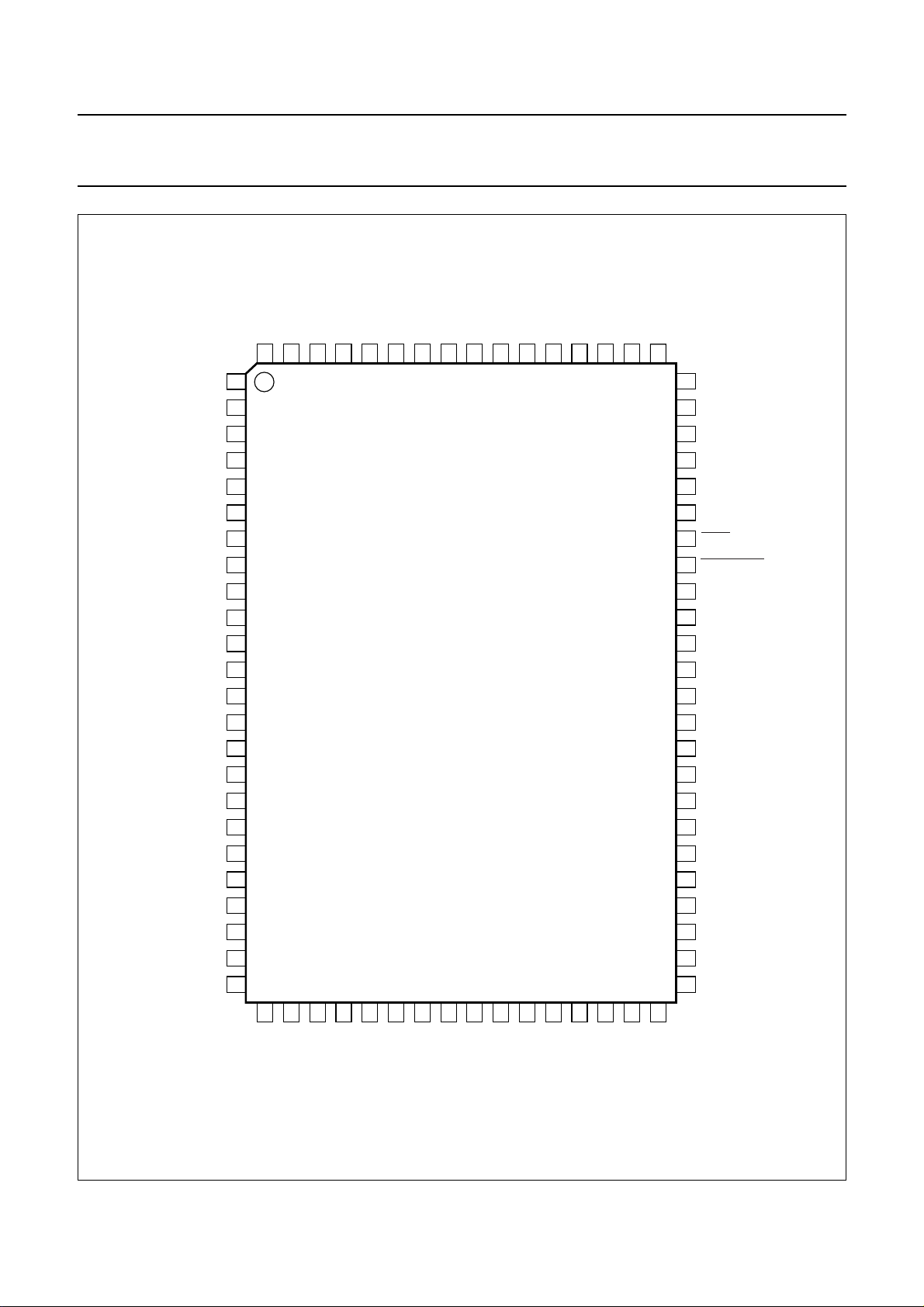
Fig.2 Pin configuration.
1999 Aug 05 10
33
34
S_IO_WS
V
2
I
35
SSD5V2
DDD5V2
V
36
37
S_IO_OUT1
S_IO_OUT2
2
2
I
I
38
39
DSP_IN1
DSP_IN2
40
MGS207
DSP_OUT1
Philips Semiconductors Preliminary specification
Sound effects DSP SAA7712H
8 FUNCTIONAL DESCRIPTION
8.1 Analog outputs
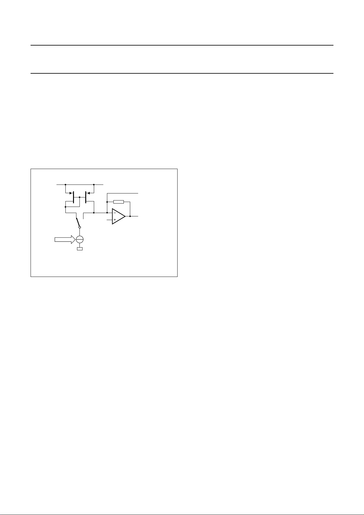
8.1.1 ANALOG OUTPUT CIRCUIT
Depending on the configuration of the equalizer sections,
the SAA7712H has 2 or 4 analog outputs which are
supplied by the samepower supply. Each ofthese outputs
hasavoltageand a current pin (see Fig.3). The signals are
available on 2 outputs (OUT0 and OUT1), or 4 outputs
(OUT0, OUT1, OUT2 and OUT3).
handbook, halfpage
BIT 0 to 13
MSB
DAC
MGS208
V
ref
OUT0_I
(OUT1_I)
OUT0_V
(OUT1_V)
8.1.3 DACS
Each of the four low noise high dynamic range DACs
consists of a signed-magnitude DAC with current output,
followed by a buffer operational amplifier.
8.1.4 UPSAMPLE FILTER
To reduce spectral components above the audio band, a
fixed 4 times oversampling and interpolating digital filter is
used. The filters give an out-of-audio-band attenuation of
at least 29 dB. The filter is followed by a first-order noise
shaper to expand the dynamic range to more than 105 dB.
The band around multiples of the sample frequency of the
DAC (4fs) is not affected by the digital filter. A capacitor
must be added in parallel with the DAC output amplifier to
attenuate this out-of-band noise further to an acceptable
level.
In Fig.4 the overall frequency spectrum at the DAC audio
output without external capacitor or low-pass filter for the
audio sampling frequencies of 38 kHz is shown. In Fig.5
the detailed spectrum around fs is shown for an fs of
38, 44.1 and 48 kHz. The pass band bandwidth (−3 dB) is
1
⁄2fs.
Fig.3 Analog output circuit.
8.1.2 DAC FREQUENCY
The sample rate (fs) of the selected source is the frame
rate of the DSP.The word clock for the upsample filter and
the clock for the DACs, at 4fs, are derived internally from
the word select of the selected audio source.
1999 Aug 05 11
Philips Semiconductors Preliminary specification
Sound effects DSP SAA7712H
MGS209
handbook, full pagewidth
α
(dB)
0
−10
−20
−30
−40
−50
−60
0 100
handbook, full pagewidth
0
α
(dB)
−10
−20
−30
−40
300 400200
Fig.4 Overall frequency spectrum audio output.
fs = 38000 Hz
f (kHz)
500
MGS210
−50
0 10000 30000
0 11605 3481623211 fs = 44100 Hz
0 12632 3789525263 fs = 48000 Hz
20000
Fig.5 Detailed frequency spectrum audio output.
1999 Aug 05 12
fs = 38000 Hz
f (Hz)
Philips Semiconductors Preliminary specification
Sound effects DSP SAA7712H
8.1.5 PERFORMANCE
The signed-magnitude noise-shaped DAC has a dynamic
range in excess of 100 dB. The signal-to-noise ratio of the
audio output at full-scale is determined by the word length
of the converter. The noise at low outputs is fully
determined by the noise performance of the DAC. Since it
is a signed-magnitude type, the noise at digital silence is
also low. As a disadvantage, the total THD is higher than
conventional DACs. The typical total harmonic
distortion-plus-noise to signal ratio as a function of the
output level is shown in Fig.6.
handbook, halfpage
−20
(THD + N)/S
(dB)
−40
MGS211
8.1.6 POWER-ON MUTE (POM)
To avoid any uncontrolled noise at the audio outputs after
power-on of the IC, the reference current source of the
DAC is switched off. The capacitor on pin POM
determines the time after which this current has a soft
switch-on.So at power-on the current audiosignal outputs
are always muted. The loading of the external capacitor is
done in two stages via two different current sources.
The loading starts at a current level that is 9 times lower
than the current loading after the voltage on pin POM has
passed the 1 V level. This results in an almost dB linear
behaviour.
8.1.7 POWER-OFF PLOP SUPPRESSION
Power should still be provided to the analog part of the
DAC, while the digital part is switching off. As a result, the
output voltage will decrease gradually allowing the power
amplifier some extra time to switch-off without audible
plops. If a 5 V power supply is present, the supply voltage
of the analog part of the DAC can be fed from the 5 V
power supply via a 1.8 V zener diode. A capacitor,
connected to the 3.3 V power supply, provides power to
the analog part when the 5 V power supply is switching off
fast.
−60
−80
−80 −60 −40 0
−20
output level (dB)
Fig.6 Typical (THD + N)/S curve as a function of
the output level.
1999 Aug 05 13

Philips Semiconductors Preliminary specification
Sound effects DSP SAA7712H
8.1.8 PIN VREFDA
With two internal resistors half the supply voltage (V
DDA2
is obtained and coupled to an internal buffer. This
reference voltage is used as DC voltage for the output
operational amplifiers and as reference for the DAC.
In order to obtain the lowest noise and to have the best
ripple rejection, a filter capacitor has to be added between
this pin and ground.
8.1.9 INTERNAL DAC CURRENT REFERENCE
As a reference for the internal DAC current and for the
DAC current source output, a current is drawn from the
level on pin VREFDA to pin V
(ground) via an internal
SSA2
resistor. The absolute value of this resistor also
determines the absolute current of the DAC. This means
that the absolute value of the current is not that fixed due
to the spread of the current reference resistor value. This,
however, does not influence the absolute output voltages
because these voltages are also derived from a
conversion of the DAC current to the actual output voltage
via internal resistors.
8.1.10 SUPPLY OF THE ANALOG OUTPUTS
All the analog circuitry of the DACs and the operational
amplifiers are fed by 2 supply pins, V
Pin V
must have sufficient decoupling to prevent THD
DDA2
DDA2
and V
SSA2
.
degradation and to ensure a good power supply rejection
ratio.
The digital part of the DAC is fully supplied from the chip
core supply.
2
8.2 I
)
8.2.1 DIGITAL DATA STREAM FORMATS
S-bus inputs and outputs
For communication with external digital sources a serial
3-line bus is used. This I2S-bus has one line for data, one
line for clock and one line for the word select.
See Fig.7 for the general waveform formats of the four
possible formats.
Theserialdigitalinputs(andoutputs)oftheSAA7712Hare
capable of handling multiple formats: Philips I2S-bus and
LSB-justified formats of 16, 18 and 20 bits word sizes.
In Philips I2S-bus format, the number of bit clock (BCK)
pulses may vary in the application. When the transmitter
word length is smaller than the receiver word length, the
receiver will fill in zeroes at the LSB side. When the
transmitter word length exceeds the receiver word length,
the LSBs are skipped. For correct operation of the DACs,
there should be a minimum of 16 bit clocks per word
select.
In the LSB-justified formats, the transmitter and receiver
must be set to the same format. Be aware that a format
switch between 20, 18 and 16 bits LSB-justified formats is
done by changing the relative timing of the word select
edges. The data bits remain unchanged. In the 20 bits
format, the 2 LSBs are zeroes. In the 16 bits format, the
2 data bits following the word select edge are not zero, but
undefined. In fact, these are the LSBs of the 18-bit word.
The timing specification for the waveforms of the serial
digital inputs and outputs are given in Fig.17.
1999 Aug 05 14
 Loading...