
INTEGRATED CIRCUITS
DATA SH EET
SAA7710T
Dolby* Pro Logic Surround
Dolby 3 stereo
Objective specification
File under Integrated Circuits, IC01
1996 Jul 17
Philips Semiconductors Objective specification
Dolby* Pro Logic Surround
Dolby 3 stereo
FEATURES
• Two stereo I2S-bus digital input channels
• Three stereo I2S-bus digital output channels
• I2C-bus mode control
• Up to 45 ms on-chip delay-line (fs= 44.1 kHz)
• Optional clock divider for crystal oscillator
• Package: SO32L
• Operating supply voltage range: 4.5 to 5.5 V.
Functions
• 4-channel active surround, 20 Hz to 20 kHz
(maximum )
• Adaptive matrix
• 7 kHz low-pass filters
• Adjustable delay for surround channel
• Modified Dolby B noise reduction
• Noise sequencer
• Variable output matrix
• Sub woofer
• Centre mode control: on/off, normal, phantom, wide
• Output volume control
• Automatic balance and master level control with
DC-offset filter
• Hall/matrix surround sound functions
2⁄
f
s
SAA7710T
• 3-band parametric equalizer on main channels left,
centre, right (fs= 44.1 kHz)
• 5-band parametric equalizer on main channels left,
centre, right (fs= 32 kHz)
• Tone control (bass/treble) on all four output channels
(fs= 44.1 kHz).
GENERAL DESCRIPTION
This datasheet describes the 103 ROM-code version of
the SAA7710T chip. The SAA7710T chip is a high quality
audio-performance digital add-on processor for digital
sound systems. It provides all the necessary features for
complete Dolby surround Pro Logic sound on chip.
In addition to the Dolby surround Pro Logic function, this
device also incorporates a 3-band parametric equalizer, a
5-band parametric equalizer, a tone control section and
volume control. Instead of Dolby Pro Logic, the surround
sound functions can be used together with the equalizer or
tone control.
QUICK REFERENCE DATA
SYMBOL PARAMETER MIN. TYP. MAX. UNIT
V
∆V
V
I
DD
I
SS
T
T
DD
DD
i
amb
stg
DC supply voltage −0.5 − 6.5 V
voltage difference between two V
pins −−550 mV
DDx
maximum input voltage −0.5 − VDD+ 0.5 V
supply current −−50 mA
supply current −−50 mA
ambient operating temperature −40 − 85 °C
storage temperature range −65 − 150 °C
Remark Dolby*: Available only to licensees of Dolby Laboratories Licensing Corporation, San Francisco, CA94111,
USA, from whom licensing and application information must be obtained. “Dolby”, the double-D symbol and “Pro Logic”
are registered trade-marks of Dolby Laboratories Licensing Corporation.
1996 Jul 17 2
Philips Semiconductors Objective specification
Dolby* Pro Logic Surround
SAA7710T
Dolby 3 stereo
ORDERING INFORMATION
TYPE NUMBER
NAME DESCRIPTION VERSION
SAA7710T/N103 SO32L plastic small outline package; 32 leads; body width 7.5 mm SOT287-1
BLOCK DIAGRAM
RTCB
22
23
24
SURROUND
CHANNEL
DELAY LINE
2
S
I
INPUT
25
27
26
17
13
3
SWITCH
CIRCUIT
TEST
data 1
+
DOLBY PRO LOGIC
OR
DOLBY 3 STEREO
OR
HALL/MATRIX
SURROUND
AUTO BALANCE
FUNCTION
I2S input 2
2
I
S_BCKIN1
2
I
S_WSIN1I2S input 1
2
S_DATAIN1
I
2
I
S_DATAIN2
2
S_BCKIN2
I
2
I
S_WSIN2
DSP_RESET
TSCAN
PACKAGE
handbook, full pagewidth
S
L
3- OR 5-BAND
C
PARAMETRIC
EQUALIZER
R
OR
TONE
SW
CONTROL
SAA7710T
VARIABLE
OUTPUT
MATRIX
I2S OUT 1
I2S OUT 2
2
I
S OUT 3
+
2
1
28
29
30
5
12
32
2
S_BCKOUT
I
2
S_WSOUT
I
2
S_DATAOUT1
I
2
S_DATAOUT2
I
2
I
S_DATAOUT3
V
DD1
V
DD2
V
DD3
I2S outputs
2
I
7
DSP_IN1
FLAG TEST
CONTROL
8
DSP_IN2
9
DSP_OUT1
DSP_OUT2
10
SDA
15
C BUS
TRANSCEIVER
16
SCL
Fig.1 Block diagram.
1996 Jul 17 3
19
V
OSCILLATOR
14
A0
OSC
20
21
XTAL
4
SHTCB
DD(XTAL)
18
V
SS(XTAL)
6
V
SS1
11
V
SS2
31
V
SS3
MGE751
Philips Semiconductors Objective specification
Dolby* Pro Logic Surround
Dolby 3 stereo
PINNING
SYMBOL PIN DESCRIPTION
2
S_WSOUT 1 I2S-bus slave word-select output
I
2
S_BCKOUT 2 I2S-bus slave bit-clock output
I
RTCB 3 asynchronous reset test control
block input (active low)
SHTCB 4 clock divider switch enable input
(low = divide)
V
DD1
V
SS1
DSP_IN1 7 flag input 1
DSP_IN2 8 flag input 2
DSP_OUT1 9 flag output 1
DSP_OUT2 10 flag output 2
V
SS2
V
DD2
TSCAN 13 scan control input
A0 14 I
SDA 15 I
SCL 16 I
DSP_RESET 17 chip reset input (active low)
V
SS(XTAL)
V
DD(XTAL)
XTAL 20 crystal oscillator output
OSC 21 crystal oscillator input
2
S_BCKIN1 22 I2S-bus master bit-clock input 1
I
2
S_WSIN1 23 I2S-bus master word-select input 1
I
2
S_DATAIN1 24 I2S-bus master data input 1
I
2
S_DATAIN2 25 I2S-bus master data input 2
I
2
S_WSIN2 26 I2S-bus master word-select input 2
I
2
S_BCKIN2 27 I2S-bus master bit-clock input 2
I
2
S_DATAOUT1 28 I2S-bus slave data output 1
I
2
I
S_DATAOUT2 29 I2S-bus slave data output 2
2
S_DATAOUT3 30 I2S-bus slave data output 3
I
V
SS3
V
DD3
5 positive power supply
6 ground power supply
11 ground power supply
12 positive power supply
2
C-bus slave address selection
input
2
C-bus serial data input/output
2
C-bus serial clock input
18 ground power supply crystal
oscillator
19 positive power supply crystal
oscillator
31 ground power supply
32 positive power supply
ndbook, halfpage
I2S_WSOUT
2
S_BCKOUT
I
DSP_OUT1
DSP_OUT2
1
2
RTCB
3
SHTCB
DSP_IN1
DSP_IN2
TSCAN
V
V
V
V
DD1
SS1
SS2
DD2
A0
SDA
SCL
4
5
6
7
8
SAA7710T
9
10
11
12
13
14
15
16
Fig.2 Pin configuration.
SAA7710T
32
31
30
29
28
27
26
25
24
23
22
21
20
19
18
17
MGE750
V
DD3
V
SS3
2
I
S_DATAOUT3
2
S_DATAOUT2
I
2
S_DATAOUT1
I
2
I
S_BCKIN2
2
S_WSIN2
I
2
S_DATAIN2
I
2
S_DATAIN1
I
2
S_WSIN1
I
2
S_BCKIN1
I
OSC
XTAL
V
DD(XTAL)
V
SS(XTAL)
DSP_RESET
1996 Jul 17 4

Philips Semiconductors Objective specification
Dolby* Pro Logic Surround
Dolby 3 stereo
FUNCTIONAL DESCRIPTION
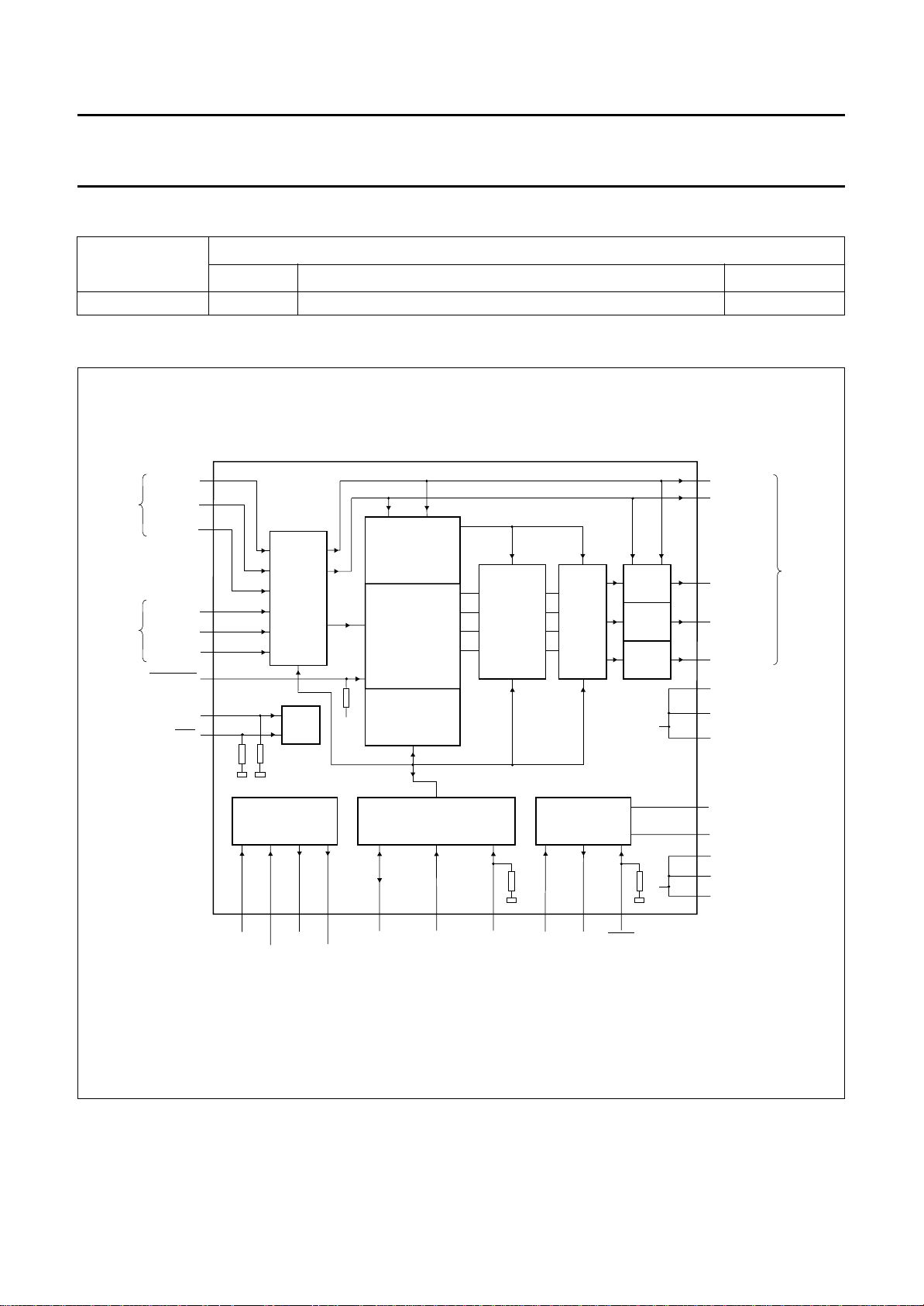
Figure 1 shows the block diagram of the SAA7710T.
The SAA7710T consists of a Dolby Pro Logic decoder
together with equalizer or tone control. The Dolby Pro
Logic part of the IC may be used to decode audio
soundtracks (Dolby surround movies or Dolby surround
video productions) from for example, a video recorder
(VCR) or a CD laser disc into four channels Left, Centre,
Right and Surround (L,C,R,S).
If desired, post-processing with either an equalizer or a
tone control section is possible. In addition to this, a Sub
Woofer (SW) channel, digital volume control and a
user-programmable variable output matrix are
implemented.
Hall/matrix surround sound functions are implemented for
material not encoded using Dolby Surround. These
features can be used as an alternative to Dolby Pro Logic
and can also be combined with the equalizer or tone
control sections.
In the I2S-bus input switch circuit a choice is made
between the possible input configurations.
SAA7710T
• Equalizer (5-band on L,C,R); variable output matrix
volume contol
• Extra sub woofer
HE DOLBY 3 STEREO MODE
T
(1)
.
In Dolby 3 stereo mode, several blocks must be initialized
and controled during operation:
• Noise generator and noise sequencer
• Centre channel mode
(1)
(normal, phantom, wide and off)
• Combining network coefficients.
HE HALL/MATRIX SURROUND MODE
T
In hall/matrix surround mode, the blocks listed below must
be initialized and controlled during operation:
• Input balance control
• Hall or matrix surround Mode setting
• All-pass and filter transfer characteristics
• 7 kHz low-pass filter in surround channel
• Surround channel delay
(1)
.
(1)
(1)
(1)
;
Functional modes
The device thus supports two main modes, Dolby Pro
Logic/Dolby 3 stereo or hall/matrix surround mode.
Both modes can be combined with equalizing (3-band or
5-band) or tone control depending on f
and available cycle
s
budget.
HE DOLBY PRO LOGIC MODE
T
In Dolby Pro Logic mode, several blocks must be initialized
and controlled during operation:
• Noise generator and noise sequencer
• Centre channel mode
(1)
(normal, phantom, wide, off)
• Combining network coefficients
• 7 kHz low-pass filter in surround channel
• Surround channel delay time
(1)
(1)
• Modified Dolby B noise reduction must be on.
Possible post-processing modes for Dolby Pro Logic are:
• Volume control only
• Equalizer (3- or 5-band on L,C,R) or tone control
(L,C,R,S); fixed output matrix
(1) The coefficient set used to initialize and control the operation
of the Dolby Pro Logic mode depends upon the selected
sampling frequency f
= 32, 44.1 or48 kHz.
s
(1)
; volume control
Possible post-processing modes for hall/matrix surround
are as above:
• Volume control only
• Equalizer (3- or 5-band on L,C,R) or tone control
(L,C,R,S); fixed output matrix
• Equalizer (5-band on L,C,R); variable output matrix
(1)
; volume control
(1)
;
volume control
• Extra sub woofer
DDITIONAL INFORMATION
A
(1)
.
The possible modes of operation are discussed in more
detail in the
Guide, Application Note AN95063
“SAA7710T Dolby Pro Logic Programming
”. This also includes
which features are available for a given system clock
frequency and sample frequency and the possible input
configurations.
Clock circuit and oscillator
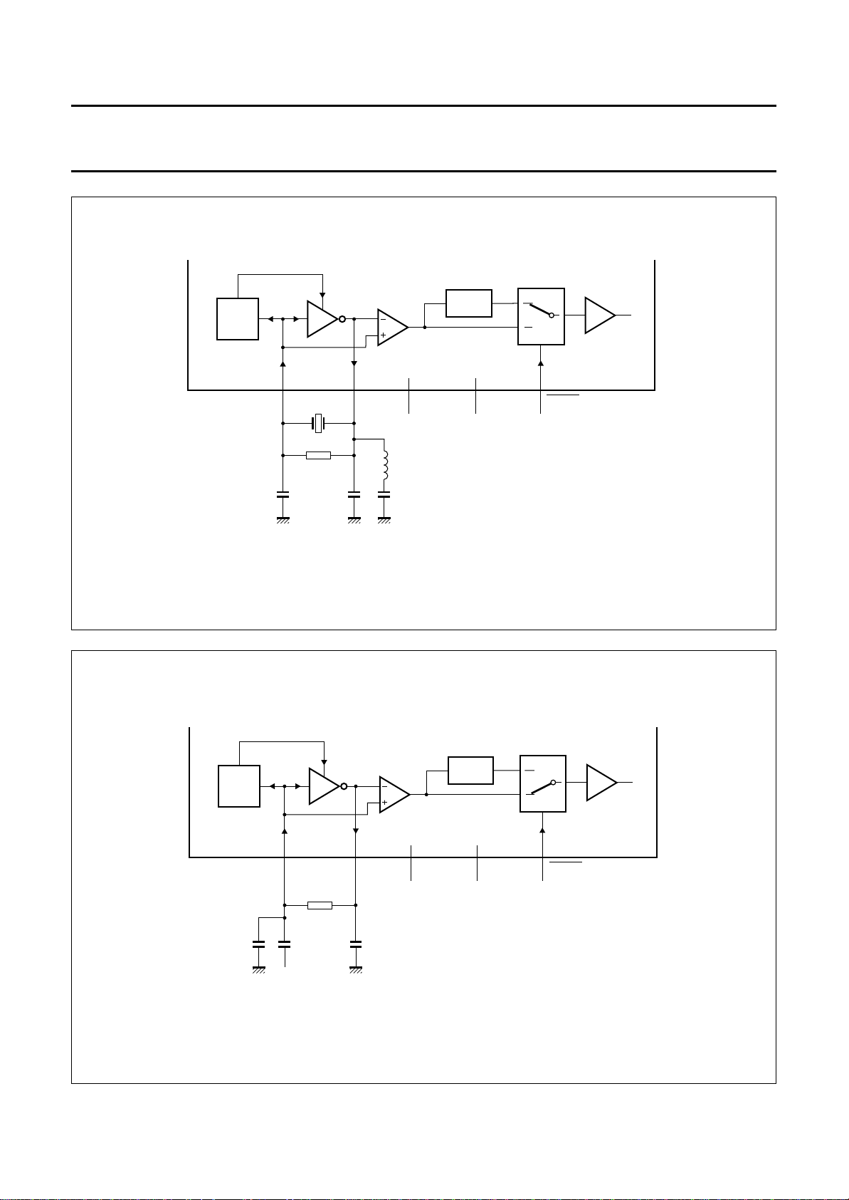
The chip has an on board crystal clock oscillator. The block
schematic of this Pierce oscillator is shown in
Figs 3 and 4. The active element needed to compensate
for the loss resistance of the crystal is the amplifier Gm.
This amplifier is placed between the XTAL (output) pin and
the OSC (sense) pin. The gain of the oscillator is internally
controlled by the automatic gain control. This prevents too
much power loss in the crystal. The higher harmonics are
1996 Jul 17 5

Philips Semiconductors Objective specification
Dolby* Pro Logic Surround
Dolby 3 stereo
then as low as possible. The signals on the OSC and XTAL
pin are differentially amplified.
The oscillator has these two modes of operation:
The crystal oscillator mode: in this mode (see Fig.3),
a quartz crystal oscillator is used to generate a clock
signal which is subsequently divided by 2 to ensure that
the final clock signal has a 50% duty-cycle.
The oscillator circuit components R
depend on the crystal. In the case of an overtone
oscillator, the ground-harmonic is filtered out by L1 and
C3.
Pin SHTCB is held low so that the divided signal is
selected. Only a quartz crystal should be used in this
mode.
The slave oscillator mode: in this mode (see Fig.4),
the oscillator circuit acts as a slave driven by a master
system clock. The clock divider can be switched on or off
using pin SHTCB. When the divider is not used, the
duty-cycle of the clock will depend on the master system
clock duty-cycle and the rising and falling edge times.
and C1, C2
bias
SAA7710T
This places a tolerance of 5% on the 50% duty-cycle of
the master system clock (see Chapter “AC
characteristics”).
In order to be able to control the phase of the clock signal
during testing the divider is skipped and the signal is
directly fed to the circuit via the multiplexer in the TEST
position.
S
UPPLY OF THE CRYSTAL OSCILLATOR
The power supply connections to the oscillator are
separated from the other supply lines to minimise
feedback from on-chip ground bounce to the oscillator
circuit. Noise on the power supply affects the AGC
operation so the power supply should be decoupled.
The V
V
DD(XTAL)
SS(XTAL)
pin is used as ground supply and the
as positive supply.
1996 Jul 17 6
Philips Semiconductors Objective specification
Dolby* Pro Logic Surround
Dolby 3 stereo
handbook, full pagewidth
AGC
ON CHIP
OFF CHIP
C1
10 pF
21
OSC
Gm
100 kΩ
R
bias
10 pF
C2
XTAL
DIVIDE
BY 2
V
DD(XTAL)VSS(XTAL)
L1
4.7 µH
C3
1 nF
SAA7710T
CLOCK
4181920
SHTCB
BUFFER
MGE752
0
1
TEST
= 0
handbook, full pagewidth
AGC
ON CHIP
OFF CHIP
40 pF
Fig.3 Block diagram Crystal Oscillator Circuit.
0
1
slave
input
21
OSC
10 pF
Gm
100 kΩ
XTAL
10 nF
DIVIDE
BY 2
V
DD(XTAL)VSS(XTAL)
TEST
= 1
4181920
SHTCB
CLOCK
BUFFER
MGE753
1996 Jul 17 7
Fig.4 Block diagram Slave Oscillator Circuit.
Philips Semiconductors Objective specification
Dolby* Pro Logic Surround
Dolby 3 stereo
I2S-bus Interfaces and system clock
2
S-BUS BASICS
I
handbook, full pagewidth
SCK
SD
WS
SCK
T
cy
tLC>= 0.35 T
tsr>= 0.2 T thr>= 0
SAA7710T
tHC>= 0.35 T
VIH (70%)
VIL (20%)
VIH (70%)
VIL (20%)
WS
SD
MSB
LEFT
Fig.5 I2S-bus timing and format.
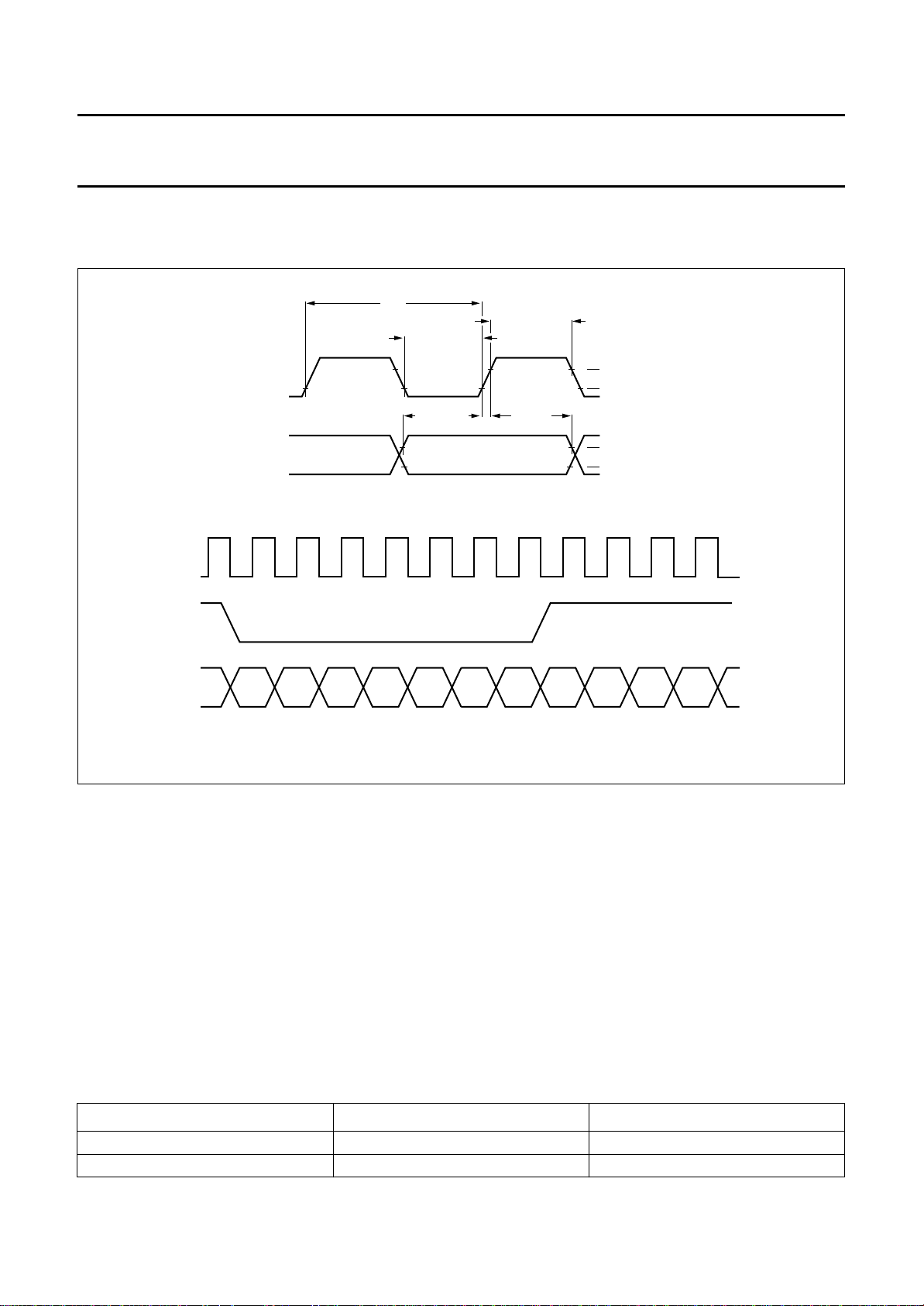
For communication with external digital sources and or
additional external processors the I2S-bus digital interface
bus is used. It is a serial 3-line bus, with one line for data,
one line for clock and one line for the word select.
Figure 5 shows an excerpt of the Philips I2S-bus
specification interface report regarding the general timing
and format of I2S-bus. Word Select (WS) logic 0 means left
channel word, logic 1 means right channel word.
The serial data is transmitted in two’s complement with the
MSB first. One clock period after the negative edge of the
word select line the MSB of the left channel is transmitted.
Data is synchronised with the negative edge of the clock
and latched at the positive edge.
MSB
RIGHT
MBH173
2
S-BUS INPUT CIRCUIT
I
The I2S-bus input circuits can be configured in the
following way using the SEL-IN1/IN2 bit (see Table 4):
1. I2S input 1 is master
(SEL-IN1/IN2 bit = logic 0(default)).
2. I2S input 2 is master (SEL-IN1/IN2 bit = logic 1)
The incoming bit-clock frequency defines the accuracy in
terms of number of bits of the incoming data samples.
The input circuit is designed to accept any number of bits
per channel up to a maximum of 18 bits. The accepted
data format is MSB-first.
Table 1 Data Accuracy in I2S-bus Interface
INCOMING DATA WIDTH I2S-BUS IN DATA WIDTH I2S-BUS OUT DATA WIDTH
A<18 A A
B≥18 18 18
1996 Jul 17 8
 Loading...