Philips saa7707h DATASHEETS

INTEGRATED CIRCUITS
DATA SH EET
SAA7707H
Car radio Digital Signal Processor
(CDSP)
Preliminary specification
File under Integrated Circuits, IC01
1996 May 22

Philips Semiconductors Preliminary specification
Car radio Digital Signal Processor
(CDSP)
CONTENTS
1 FEATURES
1.1 Hardware
1.2 Software
2 APPLICATIONS
3 GENERAL DESCRIPTION
4 QUICK REFERENCE DATA
5 ORDERING INFORMATION
6 BLOCK DIAGRAM
7 PINNING
8 FUNCTIONAL DESCRIPTION
8.1 Signal path for level information
8.2 Level ADC switch mode integrator (pin CINT)
8.3 Internal ground reference for the level ADC
(pin V
8.4 Common mode reference voltage for RDS
ADC, ADC level and buffers (pin V
8.5 Signal path for audio/MPX and stereo decoder
8.6 Mono/stereo switching
8.7 The automatic lock system
8.8 Input sensitivity for FM
8.9 Common mode reference voltage for MPX
ADC and buffers (pin V
8.10 Supply voltages for the switch capacitor DACs
of the FMMPX ADC and FMRDS ADC
(pins V
8.11 Noise level
8.12 TAPE/AUX de-multiplex
8.13 Signal-to-noise considerations
8.14 Channel separation correction
8.15 Input selection switches
8.16 Analog inputs supply
8.17 Digitally controlled sampling clock (DCS)
8.18 Survey of the DCS clock settings in different
modes
8.19 Synchronization with the core
8.20 Interference absorption circuit
8.21 IAC testing
9 ANALOG OUTPUTS
9.1 Digital-to-Analog Converters
9.2 Upsample filter
9.3 Volume control
9.4 Power-on mute
9.5 Power-off plop suppression
9.6 Internal reference buffer amplifier of the DAC
(pin V
9.7 Internal DAC current reference
9.8 Analog outputs supply
DACNL
DACNM
)
ref
)
and V
refMPX
DACPM
)
refRDS
)
)
SAA7707H
9.9 Clock circuit and oscillator
9.10 Crystal oscillator supply
9.11 External control pins
10 I2S-BUS DESCRIPTION
10.1 I2C-bus control (SCL and SDA pins)
10.2 I2S-bus description
10.3 Communication with external digital audio
sources (DCC + CD-WS/CL/Data pins)
10.4 Communication with external processors and
other devices (EXWS/CL/EXDAT1 and
EXDAT2)
10.5 Relationship between external input and
external output
10.6 RDS decoder (RDSCLK and RDSDAT)
10.7 Clock and data recovery
10.8 Timing of clock and data signals
10.9 Buffering of RDS data
10.10 Buffer interface
10.11 DSP reset
10.12 Power supply connection and EMC
11 LIMITING VALUES
12 THERMAL CHARACTERISTICS
13 DC CHARACTERISTICS
14 AC CHARACTERISTICS
15 I2C-BUS CONTROL AND COMMANDS
15.1 Characteristics of the I2C-bus
15.2 Bit transfer
15.3 START and STOP conditions
15.4 Data transfer
15.5 Acknowledge
15.6 I2C-bus format
16 SOFTWARE DESCRIPTION
17 APPLICATION INFORMATION
18 PACKAGE OUTLINE
19 SOLDERING
19.1 Introduction
19.2 Reflow soldering
19.3 Wave soldering
19.4 Repairing soldered joints
20 DEFINITIONS
21 LIFE SUPPORT APPLICATIONS
22 PURCHASE OF PHILIPS I2C COMPONENTS
1996 May 22 2

Philips Semiconductors Preliminary specification
Car radio Digital Signal Processor (CDSP) SAA7707H
1 FEATURES
1.1 Hardware
• Bitstream 3rd-order Sigma-Delta Analog-to-Digital
Converters (ADCs) with anti-aliasing broadband input
filters
• Digital-to-Analog Converters (DACs)with four times
oversampling and noise shaping
• Digital stereo decoder
• Improved digital Interference Absorption Circuit (IAC)
• RDS processing with optional 16-bit buffer via separate
channel (two-tuner radio possible)
• Auxiliary analog CD input (CD-walkman, speech,
economic CD-changer, etc.)
• Two separate full I
2
S-bus CD and DCC high
performance interfaces
• Expandable with additional Digital Signal Processors
(DSPs) for sophisticated features through an I2S-bus
gateway
• Audio output short-circuit protected
• I2C-bus controlled
• Analog tape input
• Operating ambient temperature from −40 to +85 °C.
1.2 Software
• Improved FM weak signal processing
• Integrated 19 kHz MPX filter and de-emphasis
• Electronic adjustments: FM/AM level, FM channel
separation and Dolby level
• Baseband audio processing (treble, bass, balance,
fader and volume)
• Dynamic loudness or bass boost
• Stereo one-band parametric equalizer
• Audio level meter for an automatic leveller
(in combination with microcontroller)
• Tape equalization (DCC analog playback)
• Music Search detection for Tape (MSS)
• Pause detection for RDS updates
• Dolby-B tape noise reduction
• Adjustable dynamics compressor
• CD and DCC de-emphasis processing
• Signal level, noise and multi-path detection for RDS
2
C-bus command)
(I
• Improved AM reception.
2 APPLICATIONS
• Car radio
• Car audio systems.
3 GENERAL DESCRIPTION
The SAA7707H performs all the signal functions in front of
the power amplifiers and behind the AM and FMMPX
demodulation of a car radio or the tape input.
These functions are:
• Interference absorption
• Stereo decoding
• RDS decoding
• FM and AM weak signal processing (soft mute, sliding
stereo, etc.)
• Dolby-B tape noise reduction
• The audio controls (volume, balance, fader, tone and
dynamics compression).
Some functions have been implemented in hardware
(stereo decoder, RDS decoder and IAC) and are not freely
programmable. Digital audio signals from external sources
2
with I
S-bus formats are accepted. There are four
independent analog output channels. This enables, in
special system configurations, separate tone and
equalization control for front and rear speakers.
The CDSP contains a basic program that enables a set
with:
• AM/FM reception
• Sophisticated FM weak signal functions
• Music Search detection for Tape (MSS)
• Dolby-B tape noise reduction system
• CD play with compressor function
• Separate bass and treble tone control and fader/balance
control.
For high-end sets with special and more sophisticated
features, an additional Digital Signal Processor (DSP) can
be connected. Examples of such features are:
• Noise-dependent volume control
• 10-band graphic equalizer
• Audio spectrum analyzer on display
• Signal delay for concert hall effects.
1996 May 22 3

Philips Semiconductors Preliminary specification
Car radio Digital Signal Processor (CDSP) SAA7707H
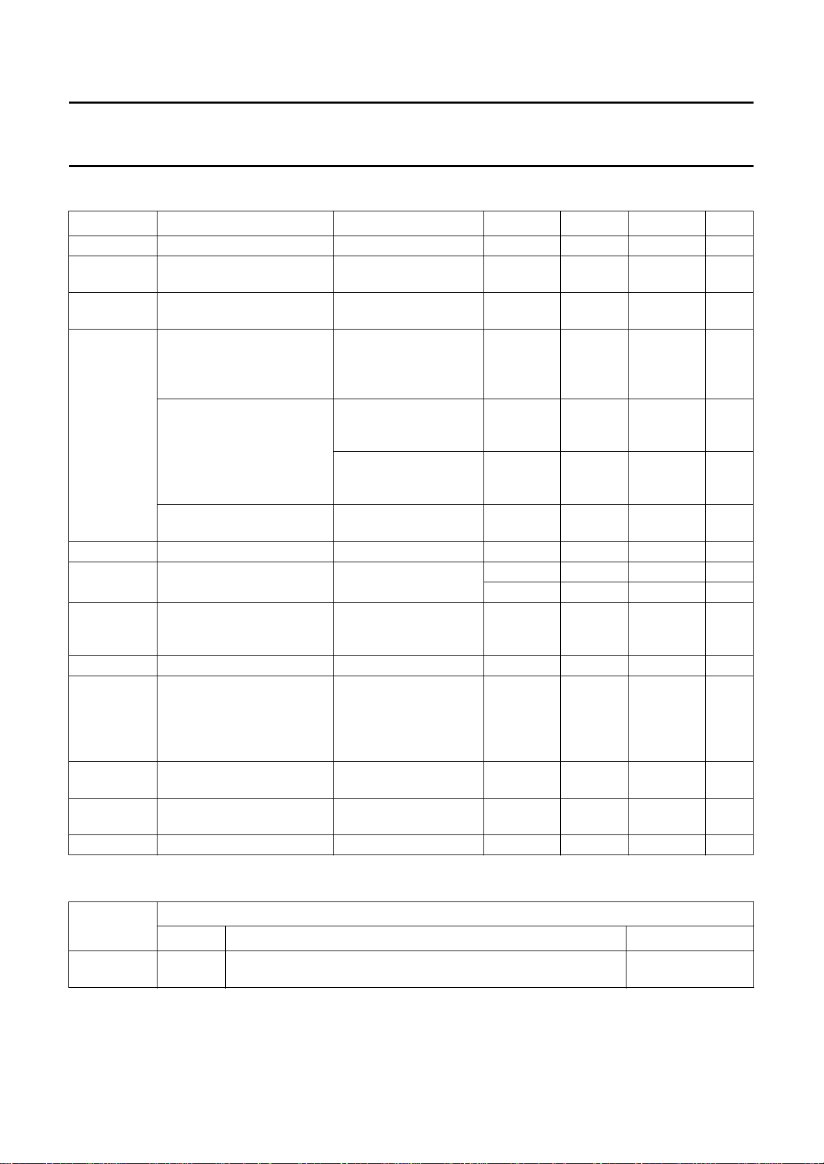
4 QUICK REFERENCE DATA
SYMBOL PARAMETER CONDITIONS MIN. TYP. MAX. UNIT
V
DDD(tot)
I
DDD(tot)
P
tot
S/N level ADC signal-to-noise
V
iFS
THD total harmonic distortion
V
imc(rms)
RES DAC resolution − 18 − bits
(THD + N)/S total harmonic distortion plus
DR dynamic range of DAC f
DS digital silence of DAC f
f
xtalDSP
total DC supply voltage all supply pins 4.75 5 5.5 V
total DC supply current maximum activity of the
DSP; f
= 36 MHz
xtal
total power dissipation maximum activity of the
DSP; f
= 36 MHz
xtal
RMS value;
ratio
unweighted;
− 160 200 mA
− 0.8 1.1 W
48 54 − dB
B=0to29kHz;
maximum input
ADC signal-to-noise ratio not multiplexed;
81 85 − dB
B = 19 kHz;
V
= 1 V (RMS)
i
multiplexed;
72 76 − dB
unweighted;
B = 19 kHz; 1 V (RMS)
ADC signal-to-noise ratio for
FM-RDS
ADC full scale input voltage V
pins 62 and 71 to 75
maximum conversion input
RMS value; B = 6 kHz;
56 −− dB
unweighted; fc=57kHz
= 4.75 to 5.5 V 1.05V
DDA1
= 1 kHz;
f
i
Vi= 1 V (RMS)
DDA1
−−71 −61 dB
− 0.03 0.09 %
1.1V
DDA1
1.15V
DDA1
V
THD < 1% 1.1 −− V
voltage level pins 62 and
71 to 75 (RMS value)
noise-to-signal ratio for DAC
and operational amplifiers
RL>5kΩAC;
Rfb= 2.7 kΩ; fi= 1 kHz;
R
=18kΩ;
ref
V
= 2.8 V (p-p);
oFS
−−70 −57 dB
maximum I2S-bus signal
= 1 kHz; −60 dB;
i
92 102 − dB
A-weighted
= 20 Hz to 17 kHz;
i
−−110 −100 dB
A-weighted
crystal frequency DSP part − 36.86 − MHz
5 ORDERING INFORMATION
TYPE
NUMBER
NAME DESCRIPTION VERSION
SAA7707H QFP80 plastic quad flat package; 80 leads (lead length 1.95 mm);
1996 May 22 4
PACKAGE
SOT318-2
body 14 x 20 x 2.8 mm

Philips Semiconductors Preliminary specification
Car radio Digital Signal Processor (CDSP) SAA7707H
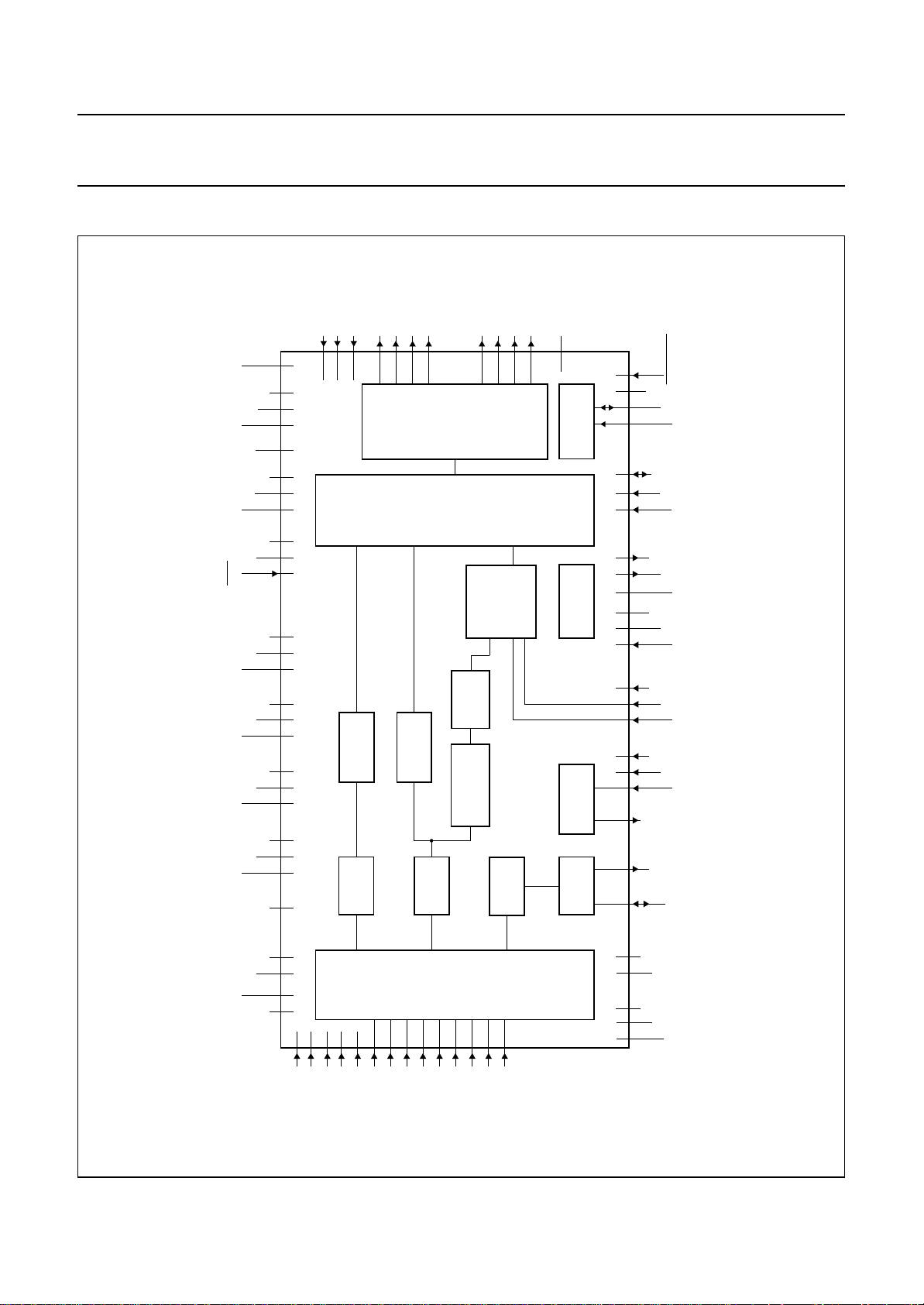
6 BLOCK DIAGRAM
ref
ref(int)
FIOL
I
V
DDD1
V
SSA
V
SSO
V
DDO
V
DDA
V
MSS/P
DEEM
MUTE
DDD4
V
DDD3
V
SSD9
V
SSD8
V
SSD6
V
SSD5
V
SSD3
V
SSD2
V
SSD1
V
DDA1
V
STEREO
DDD5
V
DDD2
V
SSD7
V
SSD4
V
SSD1
V
7
6
14
15
69
8
43
42
45
44
53
52
49
56
29 5
41
3455
54
50 51
522
EXCLK
13
20
40
SAA7707H
18
LEVEL
SIGNAL
ADC
FVOL16FIOR17FVOR
19
SIGNAL
QUALITY
ADC
RIOL
11
12
DAC
QUADRATURE
SIGNAL
DIGITAL
PROCESSOR
DIGITAL
DIGITAL
STEREO
DECODER
CIRCUIT
ABSORPTION
INTERFERENCE
RIOR10RVOR
RVOL
9
SOURCE
SELECTOR
ADC
POM
21
C-BUS
2
I
INTERFACE
DIGITALLY
CONTROLLED
CRYSTAL
OSCILLATOR
RDS
DECODER
MBH163
263938
37
27283635585759464748
SAMPLING
25
24
23
63
64616065
A0
EXWS
EXSCL
TEST1
DCCWS
CDWS
XTALO
RDSDAT
DSPRESET
SDA
SCL
EXDAT1
EXDAT2
EXDAT
SSD10
V
TEST2
DCCCLK
DCCDAT
CDDAT
CDCLK
XTALI
RDSCLK
Fig.1 Block diagram.
handbook, full pagewidth
1996 May 22 5
SSG
V
DACNL
V
SSA1
V
CINT
67 68
21
78
77
DACPM
V
70
refMPX
DACNM
V
V
80
refRDS
V
4AM62
3FM72
MPXRDS
74
AUXR
ANALOG
73
TAPEL
TAPER
SOURCE
SELECTOR
71
75
AUXL
AMAF
76
79
FMMPX
FMRDS
DDX
V
66
SSX
V
TSCAN
33 3032 31
SHTCB
RTCB

Philips Semiconductors Preliminary specification
Car radio Digital Signal Processor (CDSP) SAA7707H
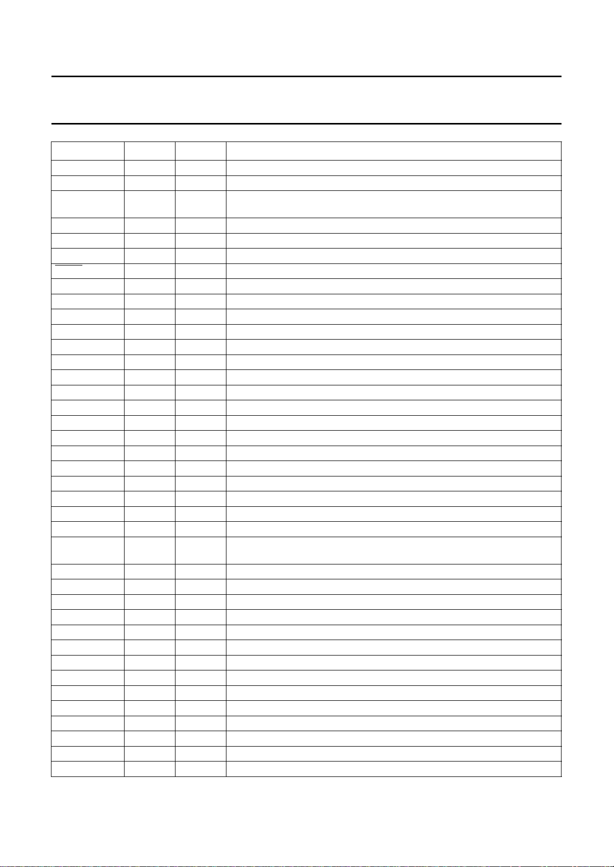
7 PINNING
SYMBOL PIN I/O DESCRIPTION
V
DACNL
CINT 2 level ADC switch-mode integrator connector
FM 3 I FM level input; via this pin, the level of the received FM radio signal is fed to
AM 4 I AM level input; via this pin, the level of the received AM radio signal is fed to
V
SSD1
V
SSA
V
DDD1
V
DDA
RIOR 9 O analog audio current output for rear right speaker
RVOR 10 O analog audio voltage output for rear right speaker
RIOL 11 O analog audio current output for rear left speaker
RVOL 12 O analog audio voltage output for rear left speaker
I
ref(int)
V
SSO
V
DDO
FIOR 16 O analog audio current output for front right speaker
FVOR 17 O analog audio voltage output for front right speaker
FIOL 18 O analog audio current output for front left speaker
FVOL 19 O analog audio voltage output for front left speaker
V
ref
POM 21 activates the Power-on mute; timing is determined with an external capacitor
V
SSD2
CDCLK 23 I clock input for CD digital audio source (I
CDWS 24 I Word Select input for CD digital audio source (I
CDDAT 25 I left/right data input for CD digital audio source (I
DSPRESET 26 I input to reset DSP core (active LOW)
EXDAT1 27 I external input data channel 1 (front) from extra DSP chip (I
EXDAT2 28 I external input data channel 2 (rear) from extra DSP chip (I
V
SSD9
TSCAN 30 scan control (active HIGH)
A0 31 I
RTCB 32 asynchronous reset test control block (active HIGH)
SHTCB 33 shift clock test control block (active HIGH)
V
SSD7
EXDAT 35 O output data for extra external DSP chip (I
EXSCL 36 O output clock for extra external DSP chip (I
EXWS 37 I/O word select input/output for extra external DSP chip (I
1 − internal ground reference voltage for the level ADC
the CDSP, the level information is required to enable correct functioning of
the weak signal behaviour
the CDSP
5 − ground supply 1 for the DACs digital circuitry
6 − ground supply for the DACs analog circuitry
7 − positive supply 1 for the DACs digital circuitry
8 − positive supply for the DACs analog circuitry
13 I internal reference current source input for the DACs
14 − ground supply for DAC output operational amplifiers
15 − positive supply for DAC output operational amplifiers
20 I voltage input for the internal reference buffer amplifier of the DAC
22 − ground supply 2 for the digital circuitry
2
S-bus)
2
S-bus)
2
S-bus)
2
S-bus)
2
S-bus)
29 − ground supply 9 for the digital circuitry
2
S-bus selection for slave sub-address
34 − ground supply 7 for the digital circuitry
2
S-bus)
2
S-bus)
2
S-bus)
1996 May 22 6

Philips Semiconductors Preliminary specification
Car radio Digital Signal Processor (CDSP) SAA7707H
SYMBOL PIN I/O DESCRIPTION
SCL 38 I serial clock input (I2C-bus)
2
SDA 39 I/O serial data input/output (I
EXCLK 40 I external reference clock input to generate 4f
used if the I2S-bus inputs are not suitable
V
SSD8
41 − ground supply 8 for the digital circuitry
STEREO 42 FM stereo indication (active HIGH)
MSS/P 43 FM pause detector/MSS detector (active HIGH); also for IAC trigger output
MUTE 44 I MUTE input pin (active LOW); only for FM mode
DEEM 45 de-emphasis; CD and DCC (active HIGH) (I
DCCCLK 46 I DCC digital audio source clock input (I
DCCWS 47 I DCC digital audio source Word Select input (I
DCCDAT 48 I DCC digital audio source left/right data input (I
V
V
V
V
V
V
V
V
DDD3
SSD3
SSD4
DDD4
DDD5
SSD5
SSD6
DDD2
49 − positive supply 3 for the digital circuitry
50 − ground supply 3 for the digital circuitry
51 − ground supply 4 for the digital circuitry
52 − positive supply 4 for the digital circuitry
53 − positive supply 5 for the digital circuitry
54 − ground supply 5 for the digital circuitry
55 − ground supply 6 for the digital circuitry
56 − positive supply 2 for the digital circuitry
TEST1 57 test pin 1 (this pin should be left open-circuit)
V
SSD10
58 − ground supply 10 for the digital circuitry
TEST2 59 test pin 2 (this pin should be left open-circuit)
RDSCLK 60 I/O radio data system bit clock input/output
RDSDAT 61 O radio data system data output
MPXRDS 62 I in FM mode, selects between FMMPX and RDSMPX input signal to the MPX
decimation filter
XTALI 63 I crystal oscillator input; can also be used as forced input in slave mode
XTALO 64 O crystal oscillator output
V
DDX
V
SSX
V
SSG
V
SSA1
V
DDA1
V
refMPX
65 − positive supply crystal circuitry
66 − ground supply crystal circuitry
67 − ground guards for ADCs
68 − analog ground supply for ADCs
69 − analog positive supply for ADCs
70 I common mode reference voltage input for MPX ADC and buffers
AUXL 71 I analog input for auxiliary left signal
AUXR 72 I analog input for auxiliary right signal
TAPEL 73 I analog input for tape left signal
TAPER 74 I analog input for tape right signal
AMAF 75 I analog input for AM audio frequency
FMMPX 76 I analog input for FM multiplex signal
C-bus)
2
S-bus)
and fas synchronization; to be
as
2
S-bus)
2
S-bus)
2
S-bus)
1996 May 22 7
 Loading...