Philips SAA7707H Datasheet

INTEGRATED CIRCUITS
DATA SH EET
SAA7707H
Car radio Digital Signal Processor
(CDSP)
Preliminary specification
Supersedes data of 1996 May 22
File under Integrated Circuits, IC01
1997 May 30

Philips Semiconductors Preliminary specification
Car radio Digital Signal Processor (CDSP) SAA7707H
CONTENTS
1 FEATURES
1.1 Hardware
1.2 Software
2 APPLICATIONS
3 GENERAL DESCRIPTION
4 QUICK REFERENCE DATA
5 ORDERING INFORMATION
6 BLOCK DIAGRAM
7 PINNING
8 FUNCTIONAL DESCRIPTION
8.1 Signal path for level information
8.2 Level ADC switch mode integrator (pin CINT)
8.3 Internal ground reference for the level ADC
(pin V
DACNL
)
8.4 Common mode reference voltage for RDS
ADC, ADC level and buffers (pin V
refRDS
)
8.5 Signal path for audio/MPX and stereo decoder
8.6 Mono/stereo switching
8.7 The automatic lock system
8.8 Input sensitivity for FM
8.9 Common mode reference voltage for MPX
ADC and buffers (pin V
refMPX
)
8.10 Supply voltages for the switch capacitor DACs
of the FMMPX ADC and FMRDS ADC
(pins V
DACNM
and V
DACPM
)
8.11 Noise level
8.12 TAPE/AUX de-multiplex
8.13 Signal-to-noise considerations
8.14 Channel separation correction
8.15 Input selection switches
8.16 Analog inputs supply
8.17 Digitally controlled sampling clock (DCS)
8.18 Survey of the DCS clock settings in different
modes
8.19 Synchronization with the core
8.20 Interference absorption circuit
8.21 IAC testing
9 ANALOG OUTPUTS
9.1 Digital-to-Analog Converters
9.2 Upsample filter
9.3 Volume control
9.4 Power-on mute
9.5 Power-off plop suppression
9.6 Internal reference buffer amplifier of the DAC
(pin V
ref
)
9.7 Internal DAC current reference
9.8 Analog outputs supply
9.9 Clock circuit and oscillator
9.10 Crystal oscillator supply
9.11 External control pins
10 I2S-BUS DESCRIPTION
10.1 I2C-bus control (SCL and SDA pins)
10.2 I2S-bus description
10.3 Communication with external digital audio
sources (DCC + CD-WS/CL/Data pins)
10.4 Communication with external processors and
other devices (EXWS/CL/EXDAT1 and
EXDAT2)
10.5 Relationship between external input and
external output
10.6 RDS decoder (RDSCLK and RDSDAT)
10.7 Clock and data recovery
10.8 Timing of clock and data signals
10.9 Buffering of RDS data
10.10 Buffer interface
10.11 DSP reset
10.12 Power supply connection and EMC
11 LIMITING VALUES
12 THERMAL CHARACTERISTICS
13 DC CHARACTERISTICS
14 AC CHARACTERISTICS
15 I2C-BUS CONTROL AND COMMANDS
15.1 Characteristics of the I2C-bus
15.2 Bit transfer
15.3 START and STOP conditions
15.4 Data transfer
15.5 Acknowledge
15.6 I2C-bus format
16 SOFTWARE DESCRIPTION
17 APPLICATION INFORMATION
18 PACKAGE OUTLINE
19 SOLDERING
19.1 Introduction
19.2 Reflow soldering
19.3 Wave soldering
19.4 Repairing soldered joints
20 DEFINITIONS
21 LIFE SUPPORT APPLICATIONS
22 PURCHASE OF PHILIPS I2C COMPONENTS
1997 May 30 2

Philips Semiconductors Preliminary specification
Car radio Digital Signal Processor (CDSP) SAA7707H
1 FEATURES
1.1 Hardware
• Bitstream 3rd-order Sigma-Delta Analog-to-Digital
Converters (ADCs) with anti-aliasing broadband input
filters
• Digital-to-Analog Converters (DACs)with four times
oversampling and noise shaping
• Digital stereo decoder
• Improved digital Interference Absorption Circuit (IAC)
• RDS processing with optional 16-bit buffer via separate
channel (two-tuner radio possible)
• Auxiliary analog CD input (CD-walkman, speech,
economic CD-changer, etc.)
• Two separate full I
2
S-bus CD and DCC high
performance interfaces
• Expandable with additional Digital Signal Processors
(DSPs) for sophisticated features through an I2S-bus
gateway
• Audio output short-circuit protected
• I2C-bus controlled
• Analog tape input
• Operating ambient temperature from −40 to +85 °C.
1.2 Software
• Improved FM weak signal processing
• Integrated 19 kHz MPX filter and de-emphasis
• Electronic adjustments: FM/AM level, FM channel
separation and Dolby level
• Baseband audio processing (treble, bass, balance,
fader and volume)
• Dynamic loudness or bass boost
• Stereo one-band parametric equalizer
• Audio level meter for an automatic leveller
(in combination with microcontroller)
• Tape equalization (DCC analog playback)
• Music Search detection for Tape (MSS)
• Pause detection for RDS updates
• Dolby-B tape noise reduction
• Adjustable dynamics compressor
• CD and DCC de-emphasis processing
• Signal level, noise and multi-path detection for RDS
2
(I
C-bus command)
• Improved AM reception.
2 APPLICATIONS
• Car radio
• Car audio systems.
3 GENERAL DESCRIPTION
The SAA7707H performs all the signal functions in front of
the power amplifiers and behind the AM and FMMPX
demodulation of a car radio or the tape input.
These functions are:
• Interference absorption
• Stereo decoding
• RDS decoding
• FM and AM weak signal processing (soft mute, sliding
stereo, etc.)
• Dolby-B tape noise reduction
• The audio controls (volume, balance, fader, tone and
dynamics compression).
Some functions have been implemented in hardware
(stereo decoder, RDS decoder and IAC) and are not freely
programmable. Digital audio signals from external sources
2
with I
S-bus formats are accepted. There are four
independent analog output channels. This enables, in
special system configurations, separate tone and
equalization control for front and rear speakers.
The CDSP contains a basic program that enables a set
with:
• AM/FM reception
• Sophisticated FM weak signal functions
• Music Search detection for Tape (MSS)
• Dolby-B tape noise reduction system
• CD play with compressor function
• Separate bass and treble tone control and fader/balance
control.
For high-end sets with special and more sophisticated
features, an additional Digital Signal Processor (DSP) can
be connected. Examples of such features are:
• Noise-dependent volume control
• 10-band graphic equalizer
• Audio spectrum analyzer on display
• Signal delay for concert hall effects.
1997 May 30 3

Philips Semiconductors Preliminary specification
Car radio Digital Signal Processor (CDSP) SAA7707H
4 QUICK REFERENCE DATA
SYMBOL PARAMETER CONDITIONS MIN. TYP. MAX. UNIT
V
DDD(tot)
I
DDD(tot)
P
tot
S/N level ADC signal-to-noise
V
iFS
THD total harmonic distortion
V
imc(rms)
RES DAC resolution − 18 − bits
(THD + N)/S total harmonic distortion plus
DR dynamic range of DAC f
DS digital silence of DAC f
f
xtalDSP
total DC supply voltage all supply pins 4.75 5 5.5 V
total DC supply current maximum activity of the
DSP; f
= 36 MHz
xtal
total power dissipation maximum activity of the
DSP; f
= 36 MHz
xtal
RMS value;
ratio
unweighted;
− 160 200 mA
− 0.8 1.1 W
48 54 − dB
B=0to29kHz;
maximum input
ADC signal-to-noise ratio not multiplexed;
81 85 − dB
B = 19 kHz;
V
= 1 V (RMS)
i
multiplexed;
72 76 − dB
unweighted;
B = 19 kHz; 1 V (RMS)
ADC signal-to-noise ratio for
FM-RDS
ADC full-scale input voltage V
pins 62 and 71 to 75
maximum conversion input
RMS value; B = 6 kHz;
unweighted; f
= 4.75 to 5.5 V 1.05V
DDA1
f
= 1 kHz;
i
=57kHz
c
Vi= 1 V (RMS)
56 −−dB
DDA1
1.1V
DDA1
1.15V
DDA1
V
−−71 −61 dB
− 0.03 0.09 %
THD < 1% 1.1 −−V
voltage level pins 62 and
71 to 75 (RMS value)
R
noise-to-signal ratio for DAC
and operational amplifiers
>5kΩAC;
L
Rfb= 2.7 kΩ; fi= 1 kHz;
R
=18kΩ;
ref
V
= 2.8 V (p-p);
oFS
−−70 −60 dB
maximum I2S-bus signal
= 1 kHz; −60 dB;
i
92 102 − dB
A-weighted
= 20 Hz to 17 kHz;
i
−−110 −100 dB
A-weighted
crystal frequency DSP part − 36.86 − MHz
5 ORDERING INFORMATION
TYPE
NUMBER
NAME DESCRIPTION VERSION
PACKAGE
SAA7707H QFP80 plastic quad flat package; 80 leads (lead length 1.95 mm);
body 14 × 29 × 2.8 mm
1997 May 30 4
SOT318-2
This text is here in white to force landscape pages to be rotated correctly when browsing through the pdf in the Acrobat reader.This text is here in
_white to force landscape pages to be rotated correctly when browsing through the pdf in the Acrobat reader.This text is here inThis text is here in
white to force landscape pages to be rotated correctly when browsing through the pdf in the Acrobat reader. white to force landscape pages to be ...
1997 May 30 5
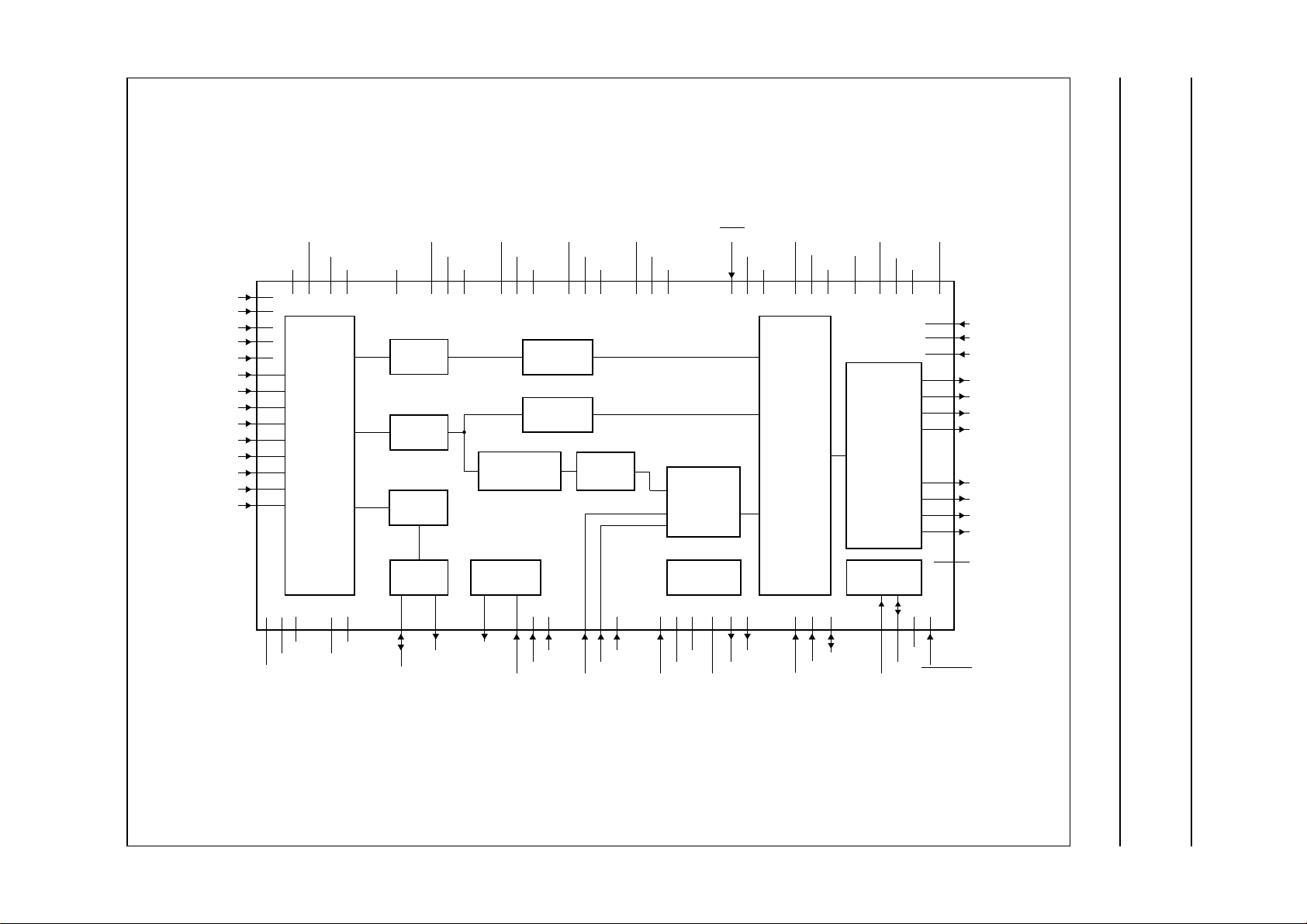
6 BLOCK DIAGRAM
Car radio Digital Signal Processor (CDSP) SAA7707H
Philips Semiconductors Preliminary specification
V
DACPM
V
DACNM
V
refMPX
V
refRDS
MPXRDS
AM
FM
AUXR
TAPER
TAPEL
AUXL
AMAF
FMMPX
FMRDS
V
DACNL
V
CINT
77
78
70
80
62
4
3
72
74
73
71
75
76
79
33 3032 31
TSCAN
SHTCB
RTCB
SSG
67 68
21
ANALOG
SOURCE
SELECTOR
66
V
SSX
V
V
SSA1
DDX
RDSCLK
V
SSD2
V
DECODER
V
SSD1
522
50 51
ADC
ADC
ADC
RDS
RDSDAT
SSD3
V
V
SSD4
INTERFERENCE
ABSORPTION
CIRCUIT
CRYSTAL
OSCILLATOR
64616065
XTALO
SSD5
V
54
XTALI
SSD6
V
SSD7
3455
QUALITY
23
63
CDCLK
SIGNAL
LEVEL
SIGNAL
24
CDWS
V
SSD8
V
41
DECODER
CDDAT
V
DDD3
V
SSD9
V
DDD2
56
29 5
DDD4
V
DDD5
52
53
49
MUTE
44
SAA7707H
DIGITAL
STEREO
DIGITAL
SOURCE
SELECTOR
DIGITALLY
CONTROLLED
SAMPLING
25
DCCWS
DCCDAT
TEST2
DCCCLK
TEST1
V
SSD10
EXDAT
DEEM
STEREO
45
EXSCL
MSS/P
V
DDA
42
PROCESSOR
43
DIGITAL
SIGNAL
EXDAT2
8
27283635585759464748
EXDAT1
V
DDA1
69
EXWS
37
V
DDO
15
QUADRATURE
INTERFACE
V
SSO
V
14
DAC
I2C-BUS
SCL
SSA
6
SDA
V
V
SSD1
A0
DSPRESET
DDD1
7
40
20
13
18
19
16
17
11
12
9
10
21
263938
EXCLK
V
ref
I
ref(int)
FIOL
FVOL
FIOR
FVOR
RIOL
RVOL
RIOR
RVOR
POM
MBH163
Fig.1 Block diagram.
handbook, full pagewidth

Philips Semiconductors Preliminary specification
Car radio Digital Signal Processor (CDSP) SAA7707H
7 PINNING
SYMBOL PIN I/O DESCRIPTION
V
DACNL
CINT 2 level ADC switch-mode integrator connector
FM 3 I FM level input; via this pin, the level of the received FM radio signal is fed to the
AM 4 I AM level input; via this pin, the level of the received AM radio signal is fed to the
V
SSD1
V
SSA
V
DDD1
V
DDA
RIOR 9 O analog audio current output for rear right speaker
RVOR 10 O analog audio voltage output for rear right speaker
RIOL 11 O analog audio current output for rear left speaker
RVOL 12 O analog audio voltage output for rear left speaker
I
ref(int)
V
SSO
V
DDO
FIOR 16 O analog audio current output for front right speaker
FVOR 17 O analog audio voltage output for front right speaker
FIOL 18 O analog audio current output for front left speaker
FVOL 19 O analog audio voltage output for front left speaker
V
ref
POM 21 activates the Power-on mute; timing is determined with an external capacitor
V
SSD2
CDCLK 23 I clock input for CD digital audio source (I
CDWS 24 I Word Select input for CD digital audio source (I
CDDAT 25 I left/right data input for CD digital audio source (I
DSPRESET 26 I input to reset DSP core (active LOW)
EXDAT1 27 I external input data channel 1 (front) from extra DSP chip (I
EXDAT2 28 I external input data channel 2 (rear) from extra DSP chip (I
V
SSD9
TSCAN 30 scan control (active HIGH)
A0 31 I
RTCB 32 asynchronous reset test control block (active HIGH)
SHTCB 33 shift clock test control block (active HIGH)
V
SSD7
EXDAT 35 O output data for extra external DSP chip (I
EXSCL 36 O output clock for extra external DSP chip (I
EXWS 37 I/O word select input/output for extra external DSP chip (I
1 − internal ground reference voltage for the level ADC
CDSP, the level information is required to enable correct functioning of the weak
signal behaviour
CDSP
5 − ground supply 1 for the DACs digital circuitry
6 − ground supply for the DACs analog circuitry
7 − positive supply 1 for the DACs digital circuitry
8 − positive supply for the DACs analog circuitry
13 I internal reference current source input for the DACs
14 − ground supply for DAC output operational amplifiers
15 − positive supply for DAC output operational amplifiers
20 I voltage input for the internal reference buffer amplifier of the DAC
22 − ground supply 2 for the digital circuitry
2
S-bus)
2
S-bus)
2
S-bus)
2
S-bus)
2
S-bus)
29 − ground supply 9 for the digital circuitry
2
S-bus selection for slave sub-address
34 − ground supply 7 for the digital circuitry
2
S-bus)
2
S-bus)
2
S-bus)
1997 May 30 6

Philips Semiconductors Preliminary specification
Car radio Digital Signal Processor (CDSP) SAA7707H
SYMBOL PIN I/O DESCRIPTION
SCL 38 I serial clock input (I2C-bus)
SDA 39 I/O serial data input/output (I
EXCLK 40 I external reference clock input to generate 4f
used if the I2S-bus inputs are not suitable
V
SSD8
41 − ground supply 8 for the digital circuitry
STEREO 42 FM stereo indication (active HIGH)
MSS/P 43 FM pause detector/MSS detector (active HIGH); also for IAC trigger output
MUTE 44 I MUTE input pin (active LOW); only for FM mode
DEEM 45 de-emphasis; CD and DCC (active HIGH) (I
DCCCLK 46 I DCC digital audio source clock input (I
DCCWS 47 I DCC digital audio source Word Select input (I
DCCDAT 48 I DCC digital audio source left/right data input (I
V
V
V
V
V
V
V
V
DDD3
SSD3
SSD4
DDD4
DDD5
SSD5
SSD6
DDD2
49 − positive supply 3 for the digital circuitry
50 − ground supply 3 for the digital circuitry
51 − ground supply 4 for the digital circuitry
52 − positive supply 4 for the digital circuitry
53 − positive supply 5 for the digital circuitry
54 − ground supply 5 for the digital circuitry
55 − ground supply 6 for the digital circuitry
56 − positive supply 2 for the digital circuitry
TEST1 57 test pin 1 (this pin should be left open-circuit)
V
SSD10
58 − ground supply 10 for the digital circuitry
TEST2 59 test pin 2 (this pin should be left open-circuit)
RDSCLK 60 I/O radio data system bit clock input/output
RDSDAT 61 O radio data system data output
MPXRDS 62 I in FM mode, selects between FMMPX and RDSMPX input signal to the MPX
decimation filter
XTALI 63 I crystal oscillator input; can also be used as forced input in slave mode
XTALO 64 O crystal oscillator output
V
DDX
V
SSX
V
SSG
V
SSA1
V
DDA1
V
refMPX
65 − positive supply crystal circuitry
66 − ground supply crystal circuitry
67 − ground guards for ADCs
68 − analog ground supply for ADCs
69 − analog positive supply for ADCs
70 I common mode reference voltage input for MPX ADC and buffers
AUXL 71 I analog input for auxiliary left signal
AUXR 72 I analog input for auxiliary right signal
TAPEL 73 I analog input for tape left signal
TAPER 74 I analog input for tape right signal
AMAF 75 I analog input for AM audio frequency
FMMPX 76 I analog input for FM multiplex signal
2
C-bus)
2
S-bus)
and fas synchronization; to be
as
2
S-bus)
2
S-bus)
2
S-bus)
1997 May 30 7

Philips Semiconductors Preliminary specification
Car radio Digital Signal Processor (CDSP) SAA7707H
SYMBOL PIN I/O DESCRIPTION
V
DACPM
V
DACNM
FMRDS 79 I analog FMMPX input for RDS decoding
V
refRDS
77 I supply voltage for the DACs switch capacitor of the FMMPX ADC and
FMRDS ADC
78 I ground supply for the DACs switch capacitor of the FMMPX ADC and
FMRDS ADC
80 I common mode reference voltage input for RDS ADC, level ADC and buffers
1997 May 30 8
Philips Semiconductors Preliminary specification
Car radio Digital Signal Processor (CDSP) SAA7707H
DDX
SSX
SSG
SSA1
DDA1
AUXL
71
refMPX
V
70
V
V
V
V
V
69
68
67
66
65
64
XTALO
XTALI
63
62
MPXRDS
61
RDSDAT
60
RDSCLK
59
TEST2
V
58
SSD10
57
TEST1
V
56
DDD2
V
55
SSD6
V
54
SSD5
V
53
DDD5
V
52
DDD4
V
51
SSD4
V
50
SSD3
V
49
DDD3
48
DCCDAT
47
DCCWS
DCCCLK
46
DEEM
45
44
MUTE
43
MSS/P
STEREO
42
V
41
SSD8
handbook, full pagewidth
V
DACNL
V
SSD1
V
V
DDD1
V
RIOR
RVOR
RVOL
I
ref(int)
V
V
FVOR
FVOL
V
SSD2
CDCLK
CDWS
CINT
FM
AM
SSA
DDA
RIOL
SSO
DDO
FIOR
FIOL
V
ref
POM
refRDS
V
FMRDS
80
79
1
2
3
4
5
6
7
8
9
10
11
12
13
14
15
16
17
18
19
20
21
22
23
24
DACNM
V
78
DACPM
V
77
AMAF
FMMPX
76
75
TAPER
TAPEL
74
73
SAA7707H
AUXR
72
25
26
27
28
29
30
31
A0
TSCAN
CDDAT
EXDAT1
DSPRESET
SSD9
V
EXDAT2
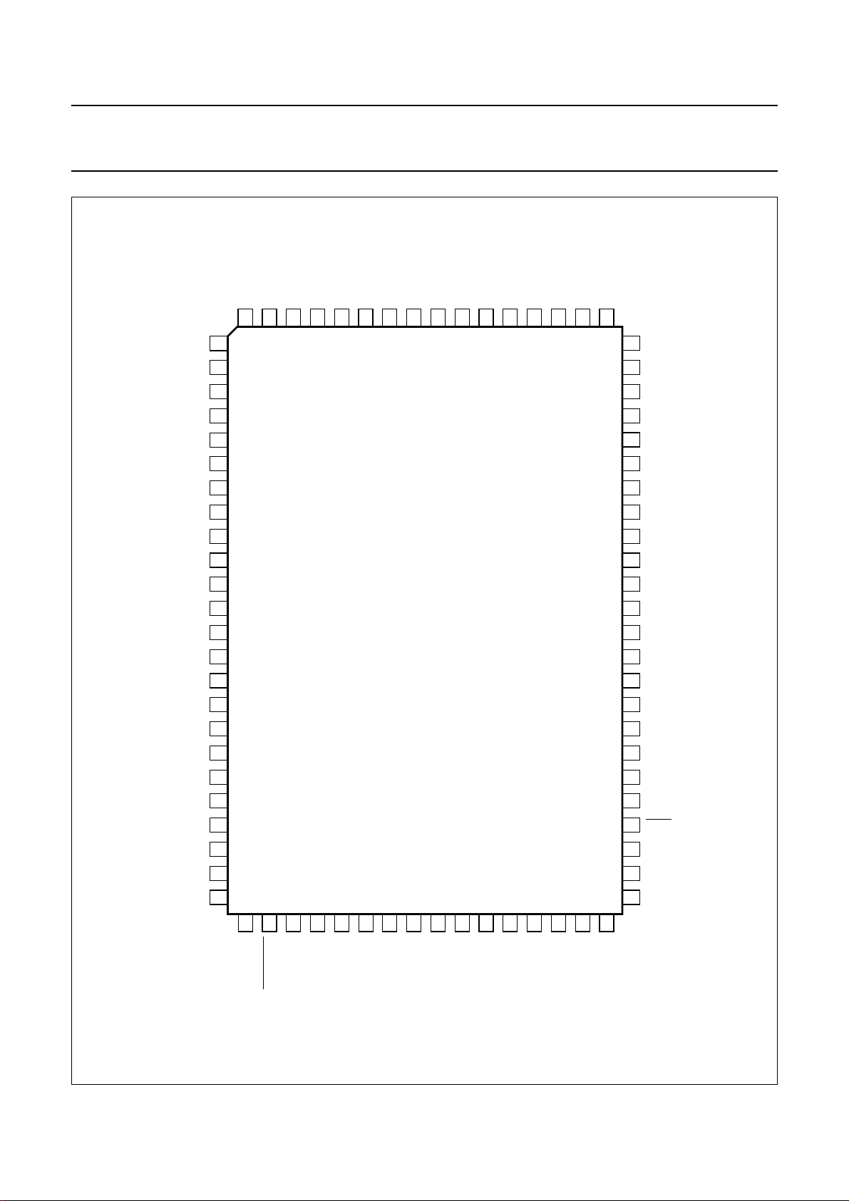
Fig.2 Pin configuration.
1997 May 30 9
32
RTCB
33
SHTCB
34
SSD7
V
35
EXDAT
36
EXSCL
37
EXWS
38
SCL
39
SDA
40
MBH162
EXCLK
Philips Semiconductors Preliminary specification
Car radio Digital Signal Processor (CDSP) SAA7707H
8 FUNCTIONAL DESCRIPTION
8.1 Signal path for level information
An FM and AM level input is implemented for FM weak
signal processing [for AM, FM and RDS search purposes
(absolute level and multi-path)]. A DC input signal is
converted by a bitstream 1st-order Sigma-Delta
analog-to-digital converter and then filtered by a
decimation filter.
The input signal has to be obtained from the radio part.
Two different circuits for AM and FM reception are
possible:
1. A circuit with two separate input signals, one for FM
level and one for AM level
2. A combined circuit with AM and FM level information
on the FM level input. The AM level input can then be
connected to another signal, which can be converted
in the non-radio mode.
The input is selected via the input selector control register.
The input signal for level control must be in the range of
0 to 5 V. The 11-bit level ADC converts this input voltage
in steps with a resolution better than 10 mV over the 5 V
range. The tolerance on the gain is less than 10%.
The MSB is always logic 0, to represent a positive level.
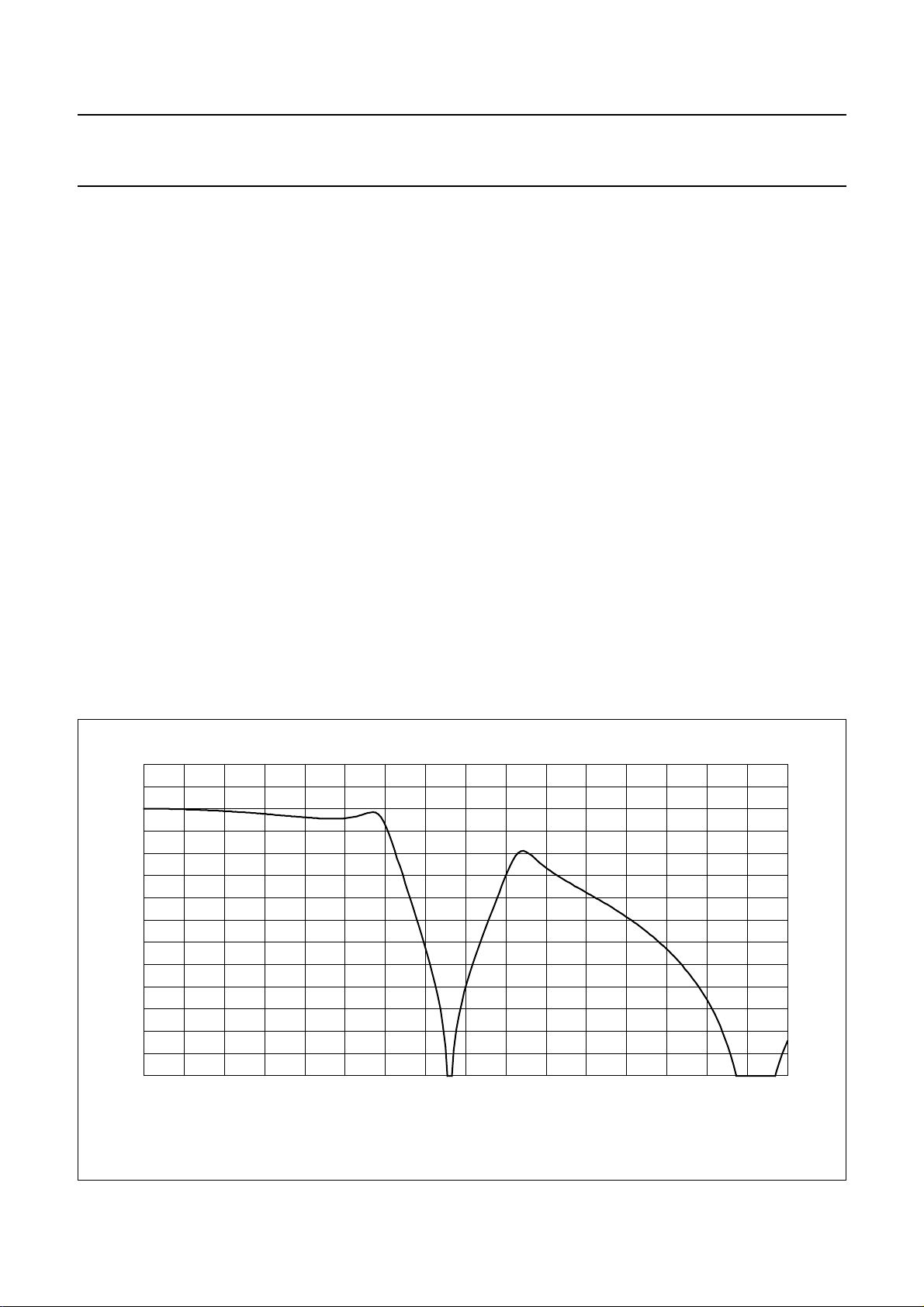
The decimation filter reduces the bandwidth of the
incoming signal to a frequency range of 0 to 29 kHz, with
a resulting sampling frequency (f
) of 76 kHz.
s
The response curve is illustrated in Fig.3.
The level information is sub-sampled by the DSP core to
obtain a field strength and a multi-path indication.
These values are stored in the coefficient or data RAM.
They can be read and used in other microcontroller
programs via the I2C-bus.
8.2 Level ADC switch mode integrator (pin CINT)
The level ADC has an internal current summation point of
the input level and the switch capacitor DAC. When used
as an integrator, an external capacitor of 1000 pF should
be connected between this pin and the analog ground at
pin V
. The summation voltage is used as an input for
SSA1
the analog-to-digital comparator level.
8.3 Internal ground reference for the level ADC
(pin V
DACNL
)
This pin serves as the internal ground reference for the
switch capacitor DAC and the level ADC and has to be
connected to the analog ground (pin V
SSA1
).
10
handbook, full pagewidth
α
(dB)
0
−10
−20
−30
−40
−50
−60
0
2010 30 40 50 60 70
Fig.3 Frequency response of the level ADC and decimation filter.
f (kHz)
MBH164
80
1997 May 30 10

Philips Semiconductors Preliminary specification
Car radio Digital Signal Processor (CDSP) SAA7707H
8.4 Common mode reference voltage for RDS
ADC, ADC level and buffers (pin V
refRDS
)
The middle reference voltage of the RDS ADC can be
filtered via this pin. This middle reference voltage is used
as a positive reference for the level ADC of the switch
capacitor DAC and as half supply reference for the RDS
ADC, the switch capacitor DACs and buffers. An external
capacitor (connected to V
) prevents crosstalk
SSA1
between the switch capacitor DACs of the RDS ADC, level
ADC and buffers, and improves the power supply rejection
ratio.
8.5 Signal path for audio/MPX and stereo decoder
The SAA7707H has four analog audio source inputs; two
single-multiplex channel inputs for AM and FM radio and
two stereo inputs for tape and auxiliary. The auxiliary input
can be used for functions such as an analog CD changer
or speech applications. The stereo inputs are multiplexed
so that they can share the same filters as the multiplexed
FM signal. The selection between the AM, FM, TAPE and
AUX input is made via the input selector control register.
The input signal behind the source selector is digitized by
a bitstream 3rd-order Sigma-Delta ADC. The first
decimation filter reduces the sample rate. This is followed
by the sample-and-hold switch of the IAC and the 19 kHz
regeneration circuit. From here, the wide-band noise
detector signal HP2 (High-Pass 2) with a frequency range
of 60 to 240 kHz is derived. A second decimation filter
reduces the output of the IAC to a lower sample rate.
This filter has two outputs, one for the multiplex signal with
a frequency range of 0 to 60 kHz (low-pass) and one for
the small-band noise detector signal HP1 (High-Pass 1)
with a frequency range of 60 to 120 kHz. The overall
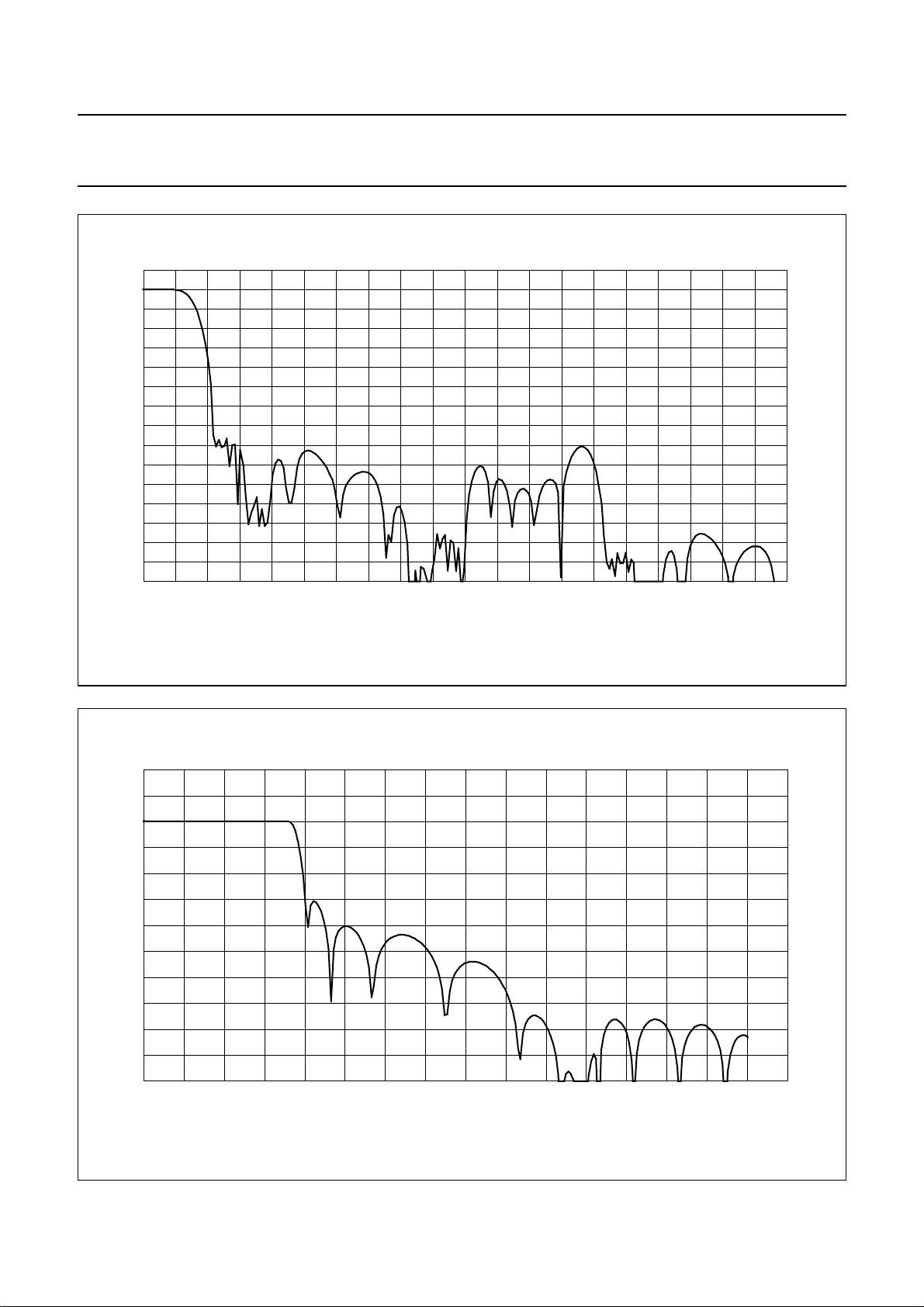
low-pass frequency response of the decimation filters is
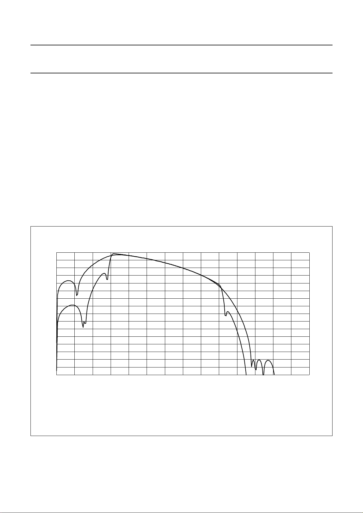
illustrated in Fig.4.
In the FM mode, the RDS ADC can be used as an input for
the MPX decimation filter. This can be selected via the
RDSMPX input at pin 62.
The outputs from this signal path to the DSP, which are all
at a sample frequency of 38 kHz, are as follows:
• Pilot presence indication: Pilot-I. This 1-bit signal is
LOW for a pilot frequency deviation of less than 4 kHz
and HIGH for a pilot frequency deviation greater than
4 kHz. It is AND locked on a pilot tone.
• Pilot quality indication: Pilot-Q. This 10-bit signal
contains information about the signal quality and is
derived from the quadrature component of the pilot-I
signal.
• ‘Left’ and ‘Right’: This is the 18-bit output of the stereo
decoder after the matrix decoding. For AM reception,
the ‘Right’ signal contains the AM-mono signal. For tape
or auxiliary signals, the output of the stereo decoder
contains sum and difference signals, but with other
crosstalk properties than on FM. Therefore, a different
matrix correction, as shown in Table 1, has to be applied
to these signals in the DSP program. The overall
frequency response of the demultiplexed signal at the
output of the stereo decoder is illustrated in Fig.5.
Table 1 Overview of the signals to the CDSP
MODE LEFT RIGHT
AM 0 mono
1
FM
TAPE/AUX
⁄2(R − L) R + L
1
⁄2(R + L) × 4/π R + L
Apart from the aforementioned theoretical response, the
non-flat frequency response of the ADC must also be
compensated for in the DSP program.
8.6 Mono/stereo switching
After division, the Digitally Controlled Sampling (DCS)
clock generates a clock signal with a frequency which is a
multiple of 19 kHz plus or minus a few Hertz. For mono
reception, the DCS circuit generates a preset frequency of
n × 19 kHz ±2 Hz. For stereo reception, the frequency is
exactly n × 19 kHz (DCS locked to n × pilot tone).
The detection of the pilot and the stereo indication is
performed in the DSP program.
8.7 The automatic lock system
The VCO operates at 19 kHz ±2 Hz exactly for no-pilot.
For stereo reception, the phase error is zero for a pilot tone
with a frequency of exactly 19 kHz. Therefore, no switch is
required to preset the clock to 19 kHz. With auxiliary
sources (tape, CD, etc.), the DCS circuit has to be preset
to a fixed value.
8.8 Input sensitivity for FM
The FM input sensitivity is optimally designed for an FM
front-end with an output voltage of 200 mV (RMS) at a
modulation depth of 22.5 kHz of a 1 kHz tone. Due to the
full-scale 1.2 V (RMS) handling capacity of the ADC, the
maximum allowed modulation depth of a transmitter, for a
THD of 10%, is 135 kHz. Full performance is possible for
transmitters with a modulation depth of up to 110 kHz.
1997 May 30 11
Philips Semiconductors Preliminary specification
Car radio Digital Signal Processor (CDSP) SAA7707H
10
handbook, full pagewidth
α
(dB)
−110
−130
−150
0
−10
−30
−50
−70
−90
0
10050 150 200 250 300 350
Fig.4 Overall frequency response multiplex ADC and decimation filters.
MBH165
f (kHz)
500400 450
20
handbook, full pagewidth
α
(dB)
0
−20
−40
−60
−80
−100
0
2010 30 40 50 60 70
Fig.5 Transfer of MPX signal at the output of the stereo decoder.
1997 May 30 12
f (kHz)
MBH166
80
Philips Semiconductors Preliminary specification
Car radio Digital Signal Processor (CDSP) SAA7707H
8.9 Common mode reference voltage for MPX ADC
and buffers (pin V
refMPX
)
The middle reference voltage of the MPX ADC can be
filtered via this pin. This middle reference voltage is used
as a half supply voltage reference for the MPX ADC,
switch capacitor DACs and buffers. An external capacitor
(connected to V
) prevents crosstalk between the
SSA1
switch capacitor DACs and buffers and improves the
power supply rejection ratio.
8.10 Supply voltages for the switch capacitor DACs
of the FMMPX ADC and FMRDS ADC
(pins V
DACNM
and V
DACPM
)
These pins are used as ground and positive supply voltage
reference for the MPX ADC, RDS ADC and the switch
capacitor DACs. For optimum performance they must be
connected directly to V
10
handbook, full pagewidth
α
(dB)
0
−10
−30
SSA1
and V
DDA1
.
8.11 Noise level
The High-Pass 1 (HP1 or narrow-band noise level filter)
output of the second MPX decimation filter, in a frequency
band from 60 to 120 kHz, is detected with an envelope
detector and decimated to a frequency of 38 kHz.
The response time of the detector is 100 ms.
Another option is the High-Pass 2 (HP2 or wide-band
noise level filter). This output from the first MPX decimation
filter is in a frequency band from 60 to 240 kHz. It has the
same properties as the HP1 and is also decimated to
38 kHz. Which signal is used (HP1 or HP2) is determined
by the input selector control register. The noise level can
be detected and filtered in the DSP core and can be used
to optimize the FM weak-signal processing. The transfer
curves of both filters before decimation are illustrated in
Fig.6.
MBH167
−50
−70
−90
−110
−130
−150
0
(1) Narrow-band noise level filter.
(2) Wide-band noise level filter.
10050 150 200 250 300 350
Fig.6 Frequency response of noise level before decimation.
1997 May 30 13
(1)(2)
f (kHz)
Philips Semiconductors Preliminary specification
Car radio Digital Signal Processor (CDSP) SAA7707H
8.12 TAPE/AUX de-multiplex
The auxiliary and tape inputs also use the stereo decoder.
Because of this, the left and right channels are multiplexed
with a 38 kHz square wave to obtain a signal similar to the
FM multiplexed signal. Auxiliary inputs can be e.g.
TV-sound, remote players (tape deck, CD-changer with
analog output etc.). The signal-to-noise ratio from such
sources is limited by the ADC in the SAA7707H (>75 dB).
The decimation filter of the ADC attenuates the harmonic
signals from this stereo encoder. For an optimum channel
separation, the 38 kHz switch signal has to be phase
corrected to compensate for the delay of the ADC and
decimation filters. This can be adjusted with the 3-bit group
delay compensation in the IAC control register. Signal
frequencies above 19 kHz at the input of the multiplexer
are converted to the audio base-band and are therefore
not allowed.
8.13 Signal-to-noise considerations
Due to the pre-emphasis of FM broadcasts, the theoretical
signal-to-noise ratio is approximately 3 dB higher for FM
stereo in comparison with multiplexed inputs.
To avoid aliasing into the tape channel, the tape noise from
the pre-amplifier must be attenuated before
analog-to-digital conversion with a 1st-order 10 kHz
low-pass filter. The frequency response is equalized after
the stereo decoder in the DSP program before the Dolby
decoder software. Using this filter, the signal-to-noise ratio
of this channel is degraded by 3 dB. This results in a
signal-to-noise ratio that is overall 6 dB lower than a tape
input with respect to FM stereo.
8.14 Channel separation correction
The channel separation is approximately 50 dB at 1 kHz
and 35 dB at 15 kHz. Because the frequency response of
the ADC has some deviation from the flat curve around
38 kHz, a perfect channel separation cannot be obtained.
Therefore, the de-multiplexed signal is corrected for
crosstalk in the DSP program.
8.15 Input selection switches
A schematic diagram of the input selection is illustrated in
Fig.5. The input selection is controlled by bits in the input
selector control register. The relationship between these
bits and the switches is indicated in Table 2.
Table 2 Analog input selection
2
I
C-BUS SELECTION
BIT
AM/FM
AUX/
RADIO
TAPE/
AUX
SFM SAM SAUX SAUX
SWITCH
00x1000
10x0100
x100010
x110001
8.16 Analog inputs supply
The analog input circuit has its own separate power supply
connections to allow maximum filtering. These pins are
V
for the analog ground and V
SSA1
power supply. V
is the connection to the guard ring
SSG
for the analog
DDA1
which isolates the analog part from the digital filters.
This pin has to be connected to the analog ground.
8.17 Digitally controlled sampling clock (DCS)
The crystal clock generates a continuous clock signal for
the internal DSP core. In the radio mode, the stereo
decoder, the RDS decoder, the ADCs and the level
decimation filters have to run synchronously with the
19 kHz pilot. Therefore, a clock signal with a controlled
frequency with a multiple of 19 kHz
(9.728 MHz = 512 × 19 kHz) is required.
In the SAA7707H, the patented method of a
non-continuous digitally controlled sampling clock has
been implemented. A frequency of 9.728 MHz is
generated by a special dividing mechanism of the master
crystal clock. Since the dividing mechanism is fixed, only a
crystal frequency of 36.86 MHz can be used.
The DCS system is controlled by up/down information
from the stereo decoder. For mono transmissions, the
DCS clock is still controlled by the stereo decoder loop.
The output keeps the DCS free-running at a multiple
frequency of 19 kHz ±2 Hz. In TAPE/AUX and AM mode,
the DCS clock must always be put in preset mode by the
input selector control register.
1997 May 30 14

Philips Semiconductors Preliminary specification
Car radio Digital Signal Processor (CDSP) SAA7707H
8.18 Survey of the DCS clock settings in different modes
The DCS clock behaves as shown in Table 3.
Table 3 DCS clock/mode
MODE DCS CLOCK
FM stereo locked on 19 kHz pilot of received
FM signal
FM mono free running
AM analog inputs
TAPE/AUX
2
I
C-bus inputs
DCC/CD
8.19 Synchronization with the core
A 38 kHz synchronization signal is derived from the DCS
clock and divided by 256.
If the external I
of the Word Select input signal is used to synchronize with
the core.
2
S-bus DCC CD is selected, the rising edge
fixed preset
fixed preset
8.20 Interference absorption circuit
The Interference Absorption Circuit (IAC) detects and
suppresses ignition interference. This hardware IAC is a
modified and digital version of the analog circuit that has
already been in use for many years.
The input signal to the IAC circuit is derived from the output
signal of the decimation filter. The interference detector
analyses the high frequency content of this MPX signal.
The discrimination between interference pulses and other
signals is performed by a special Philips patented fuzzy
logic-like algorithm and is based on probability
calculations. This logic will send appropriate pulses to an
MPX mute switch.
At Power-on, the nominal setting for an IAC with good
performance characteristics is selected (all IAC control bits
are 0). If an adjustment is needed, the characteristics can
be adapted as described in the application manual.
8.21 IAC testing
The internal IAC trigger signal is visible on the MSS/P pin
(pin 43) if the IAC trigger output bit of the IAC control
register is set. In this mode, the effect of the parameter
settings on the IAC performance can be verified.
1997 May 30 15
 Loading...